Full Range Capacitor Voltage Balance PWM Strategy for Diode-Clamped Multilevel Inverter

School of Electrical Engineering and Automation, Hefei University of Technology, Hefei 230000, China
*
Author to whom correspondence should be addressed.
Electronics 2020, 9(8), 1263; https://doi.org/10.3390/electronics9081263
Submission received: 17 July 2020
/
Revised: 3 August 2020
/
Accepted: 3 August 2020
/
Published: 6 August 2020
(This article belongs to the Section Power Electronics)
Abstract
:This paper briefly reviews virtual space vector pulse width modulation (VSVPWM) for the diode-clamped multilevel inverter (DCMLI). Based on the universal modulation model of the DCMLI with N-level, a modulation strategy named as full range capacitor voltage balance PWM (FRCVBPWM) is proposed, which has similar capacitor voltage balance characteristics as VSVPWM. The characteristic of FRCVBPWM is that there are respectively zero, N − 1 and N − 2 switching actions for the three phases of the DCMLI. Therefore, the total switching actions are greatly decreased compared with VSVPWM. The switching loss comparison between FRCVBPWM and VSVPWM is conducted by comprehensive simulations. Finally, the feasibility and superiority of FRCVBPWM over VSVPWM is verified by experiments.
1. Introduction
Recently, power electronic technology has rapidly developed in large capacity and low loss applications. The diode clamped multilevel inverter (DCMLI) was proposed [1,2], due to the advantages of lower output voltage distortion, lower electromagnetic interference and lower voltage stress [3]. This topology has received much attention and is widely used in the fields of new energy power generation, motor drives, and power quality and compensation [4,5]. Among DCMLIs, the diode clamped three-level inverter, also known as a neutral point clamped three-level inverter (NPC TLI), has been widely applied.
Capacitor voltage balance is a key issue for the DCMLI’s safe and stable operation. For an NPC TLI, some PWM strategies have been suggested for capacitor voltage control, where the carrier-based PWM (CBPWM) and space vector PWM (SVPWM) [6,7,8,9] are the two important types. It is revealed in literatures [10,11] that the relationship between a CBPWM and an SVPWM is essentially equivalent, since SVPWM can be achieved by injecting a specific zero-sequence voltage into the modulation wave of the CBPWM. However, the disadvantage of all the above methods is the low frequency oscillation on the capacitor voltage under high modulation index (MI) and low power factor (PF) operating conditions.
When the level number of the DCMLI is more than three, there are few PWM strategies for capacitor voltage control. Based on the predictive current control, an approach for a five-level DCMLI is presented [12,13], which can control both the output current and capacitor voltage. In [14,15], the passive front-end capacitor voltage balance control for a DCMLI is proposed. In [16,17], the SVPWM modulation strategy for a DCMLI is studied, but there is a problem of capacitor voltage fluctuation. For a five-level DCMLI, improved PWM strategies or an additional capacitor voltage control circuit can be adopted to control the capacitor voltage balance [18,19]. However, the increased complexity and cost of the system are the main drawbacks when applying an additional capacitor voltage control circuit.
To achieve capacitor voltage balance over the full range of the PF and the MI, a virtual SVPWM (VSVPWM) strategy is proposed [20]. This modulation strategy exhibits excellent characteristics in capacitor voltage balance control. An improved VSVPWM was presented in [21,22] to meet the other requirements of the system, such as low switching loss and reduced common-mode voltage. In addition, VSVPWM can be extended from three-phase three-level to N-level [23]; the total number of switching actions is 3N − 5. Compared to CBPWM and SVPWM, VSVPWM has the disadvantage of large switching losses, especially when the PF is low.
A PWM strategy for a DCMLI that achieves the same goals as VSVPWM, but overcomes the shortcoming of VSVPWM, is presented in this paper. Under this strategy, the full range capacitor voltage balance control can be realized. It is called a full range capacitor voltage balance PWM (FRCVBPWM), which is characterized by one phase without switching action, one phase with N − 1 switching actions, and one phase with N − 2 switching actions. In total, there are 2N − 3 switching actions for the three phases, which significantly reduce the switching losses compared to VSVPWM.
2. DCMLI and its Modulation Model
2.1. DCMLI
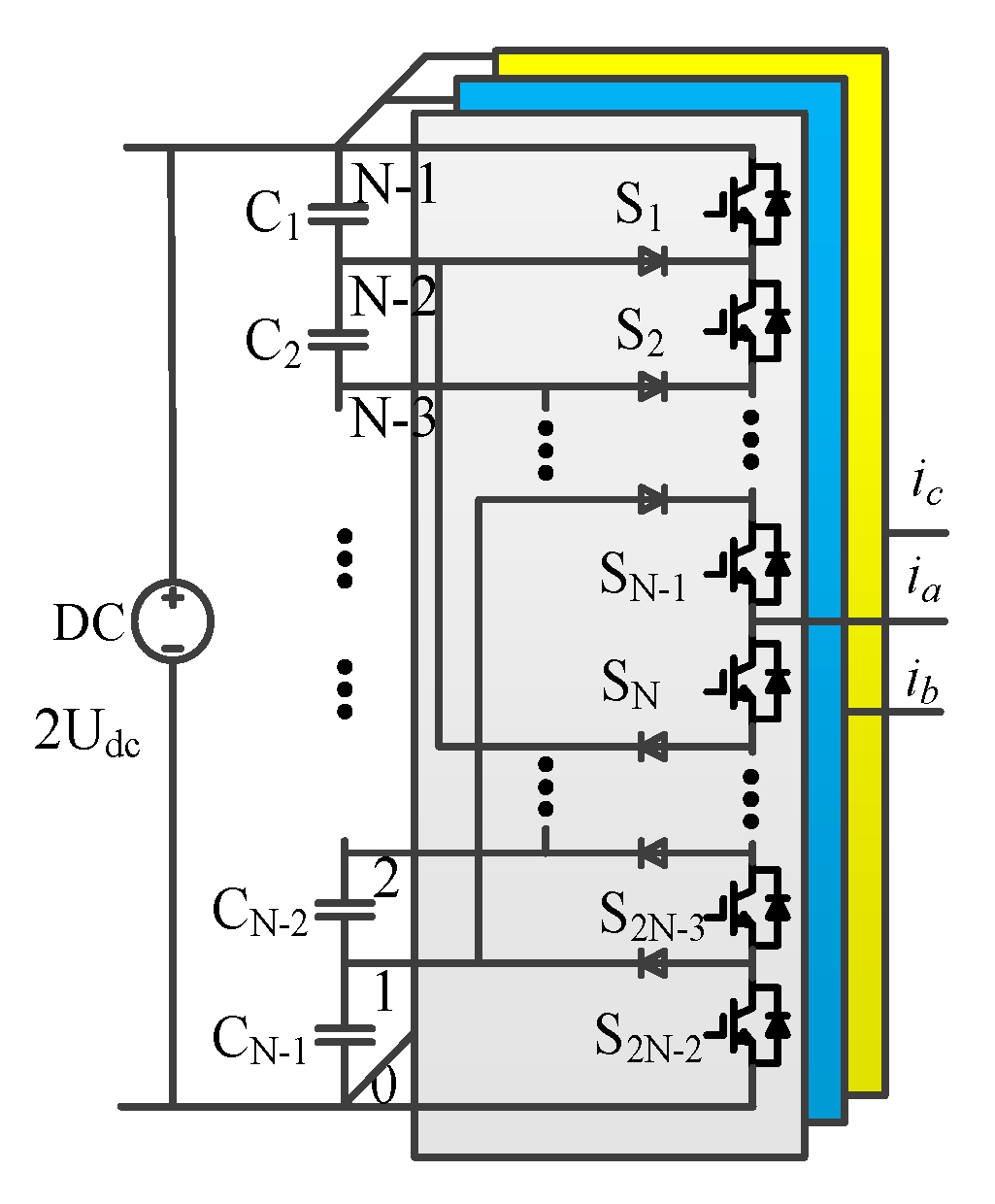
The topology of an N-level DCMLI is shown in Figure 1. There are 2N – switching devices with an anti-parallel diode and 2N – 4 clamping diodes in each phase. The capacitors C1 to CN–1 divide the DC side voltage equally when the capacitor voltage maintains balance, i.e., Uc1 = ... = Ucn–1 = 2udc/(N − 1). Level N − 1 is defined as when switches S1 – SN – 1 are turned on and the DCMLI’s output voltage is udc; Level N − 2 is defined as when switches S2 – SN are turned on and the output voltage is udc× (N − 3)/(N − 1), etc. Level 0 is defined as when switches SN – S2N − 2 are turned on and the output voltage is −udc. Hereafter, udc = 1 is assumed for simplicity and the positive current direction is considered as flowing from the inverter to the load. The normalized three-phase output voltages ua, ub and uc can be expressed as:
where, m ∊ [0, 1.1547] stands for the MI and ωt stands for the phase angle of phase A. The three-phase currents ia, ib and ic can be expressed as:
where, Im stands for the peak value of the phase current and φ ∊ [0, 2π] stands for the PF angle of the load.
2.2. The PWM Model for DCMLI
The three-phase voltages given by (1) can be rearranged as:
where, the maximum, middle and minimum phase voltages are denoted as umax, umid and umin, respectively. The phase currents corresponding to umax, umid and umin are denoted as imax, imid and imin, respectively. The general modulation model of the DCMLI, based on volt-second equilibrium is give as follows:
where,
, and . The term dkn is the duty ratio of level n of phase k (k = max, min, mid and n = 0, 1, …, N − 1). From (4), it can be seen that the relationship between the outputted line-to-line voltages and the duty ratios is revealed by the first two equations and the sum of all duty ratios of each phase must be equal to one, which is revealed by the latter three equations. The restrictive condition of dkn can be expressed as:
A specific modulation strategy can be determined by solving for the unknowns dkn given by (4). According to (4), the number of unknowns dkn is 3N but there are only five equations, therefore the specific solution of dkn cannot be obtained. For the purpose of the specific solution of dkn, additional restrictive conditions are required. In one switching cycle, the three-phase currents are assumed to be constant. To maintain each capacitor voltage balance in one switching cycle, the sum of the currents injected into each capacitor should be zero. The mathematical expression is written as:
Combining (4) with (6), the capacitor voltage balance model for the DCMLI can be further obtained. Although there are N − 2 equations based on (6), the specific solution of all duty ratios cannot be obtained, and the additional restrictive conditions are still required.
2.3. Review of VSVPWM for DCMLI
Since ia + ib + ic = 0 is always satisfied with the star-connected load, the simplest solution for (6) is:
assuming that:
The characteristics of VSVPWM can be described as follows. The phase corresponding to umax has the switching sequence composed of levels 1,…, N − 1; the phase corresponding to umin has the switching sequence composed of levels 0,…, N − 2; and the phase corresponding to umid has the switching sequence composed of levels 0,…, N − 1. According to the above characteristics, (9) can be obtained:
A complete calculation model of VSVPWM for a DCMLI can be acquired by combining (4), (8), (9) and (10), and the specific solution of all duty ratios is obtained as following:
The following conclusion can be obtained from (11). (i) All duty ratios are independent of the phase currents. (ii) When m ∊ [0, 1.1547], (5) is satisfied for all duty ratios. (iii) The condition for maintaining the voltage balance of each capacitor in one switching cycle given by (6) is satisfied. Although VSVPWM exhibits excellent capacitor voltage balance performance over the full range of PFs and MIs, the total of 3N − 5 switching actions results in large switching losses, which is a major drawback.
3. The Proposed FRCVBPWM for DCMLI
3.1. The Proposed FRCVBPWM
In this paper, FRCVBPWM is proposed to solve the problem of the large switching losses of VSVPWM. Assume that one phase has no switching action, one phase has N − 1 switching actions, and one phase has N − 2 switching actions; then there are only 2N – 3 switching actions for the three phases in one switching cycle. This is the basic idea for FRCVBPWM proposed in this paper. There are four cases, as listed in Table 1.
3.2. The Duty Ratio Calculation under Different Modes in One Switching Cycle
(a). Mode 1: MAX_PB/MID_N – 1/MIN_N – 2
In this mode, the phase corresponding to umax is clamped to level N − 1 (i.e., positive bus) without a switching action. Therefore, the duty ratios with respect to umax are written as
For umid, the switching sequence is composed of levels 0,..., N − 1 and there are N − 1 switching actions; for umin, the switching sequence is composed of levels 0,..., N − 2 and there are N − 2 switching actions. Since there is no level N − 1 in the switching sequence for umin, dmin,N − 1 is determined as:
Thus, (7) is rewritten as:
Letting and , so:
Therefore, the calculation model of FRCVBPWM for the DCMLI can be acquired by combining (4), (12)–(15), and the specific solution of all duty ratios is listed in Table 2.
(b). Mode 2: MAX_PB/MIN_N − 1/MID_N − 2
In this mode, the phase corresponding to umax is clamped to level N − 1 without a switching action. For umin, the switching sequence is composed of levels 0,..., N − 1 and there are N − 1 switching actions. For umid, there are N − 2 switching actions. There are two cases for the switching sequence of umid:
Mode 2-1: the switching sequence of umid is composed of levels 1..., N − 1.
Mode 2-2: the switching sequence of umid is composed of levels 0..., N − 2.
(c). Mode 3: MIN_NB/MAX_N − 1/MID_N − 2
In this mode, the phase corresponding to umin is clamped to level 0 (i.e., negative bus) without a switching action. For umax, the switching sequence is composed of levels 0,..., N − 1 and there are N − 1 switching actions. For umid, there are N − 2 switching actions. It also has two cases for the switching sequence of umid:
Mode 3-1: the switching sequence of umid is composed of levels 1..., N − 1.
Mode 3-2: the switching sequence of umid is composed of levels 0 ..., N − 2.
(d). Mode 4: MIN_NB/MID_N − 1/MAX_N − 2
In this mode, the phase corresponding to umin is clamped to level 0 without a switching action. For umid, the switching sequence is composed of levels 0,..., N − 1 and there are N − 1 switching actions. For umax, the switching sequence is composed of levels 1,..., N − 1 and there are N − 2 switching actions.
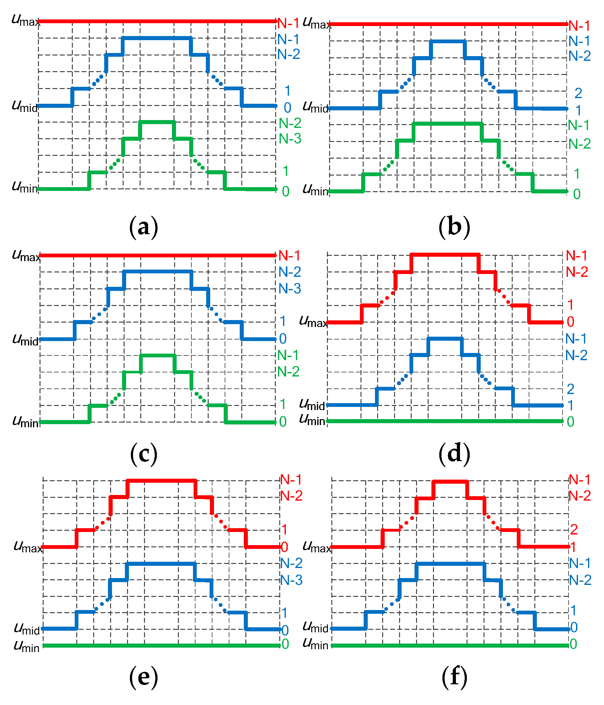
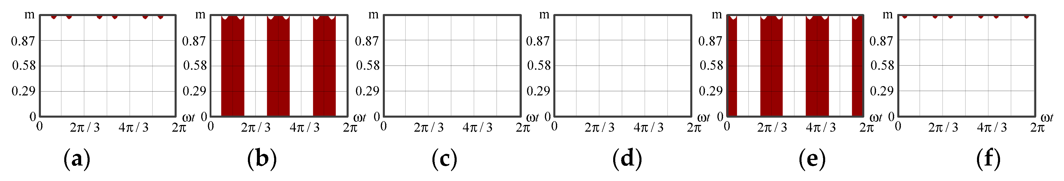
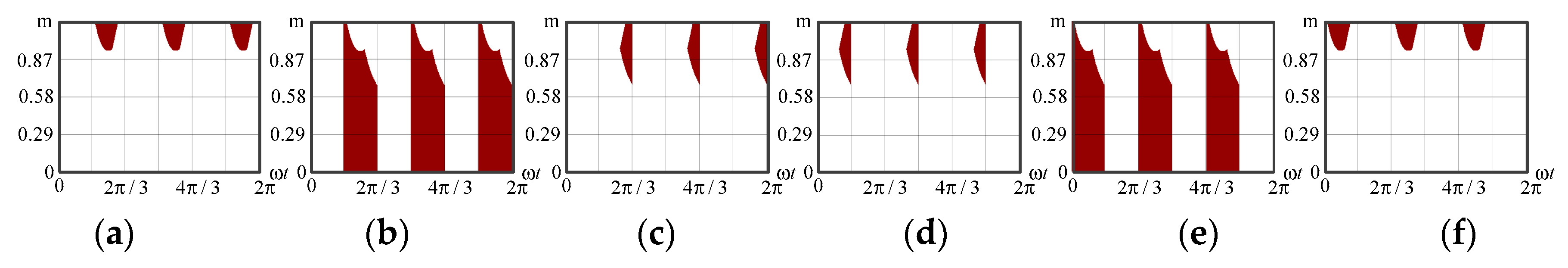
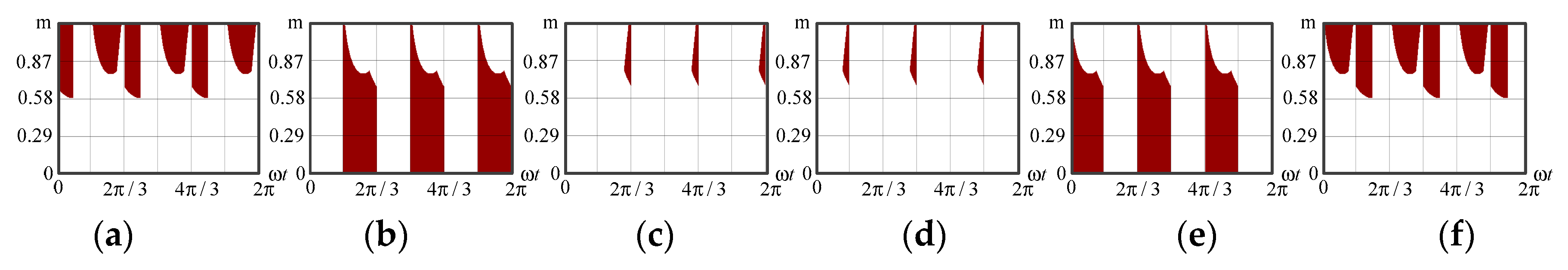
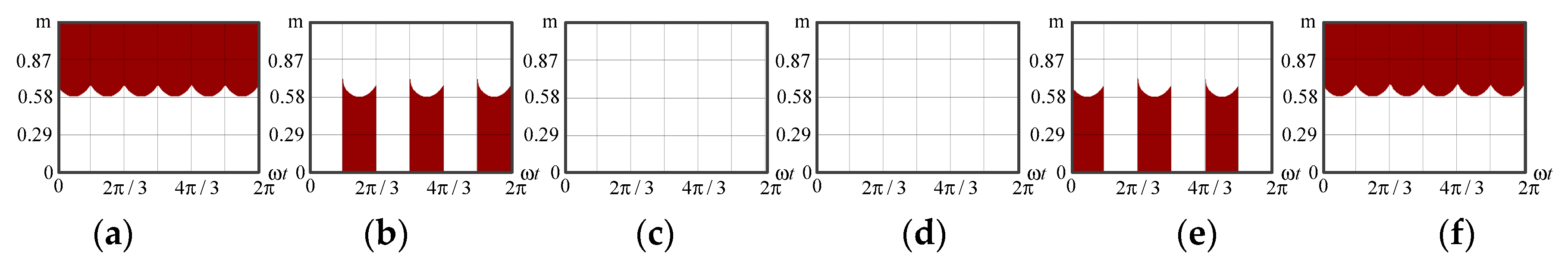
The switching sequences of the three phases under different modes are presented in Figure 2. The calculation models of all duty ratios for FRCVBPWM under different modes are presented in Table 2. It can be noted that the duty ratios under different modes are determined by the three-phase voltages and currents. The mode is available if the calculated duty ratios under this mode satisfy (6). The application area of one mode means that the mode is available within the area. The application areas under several certain φ under different modes are shown in Figure 3, Figure 4, Figure 5 and Figure 6, where the white areas stand for the application areas.
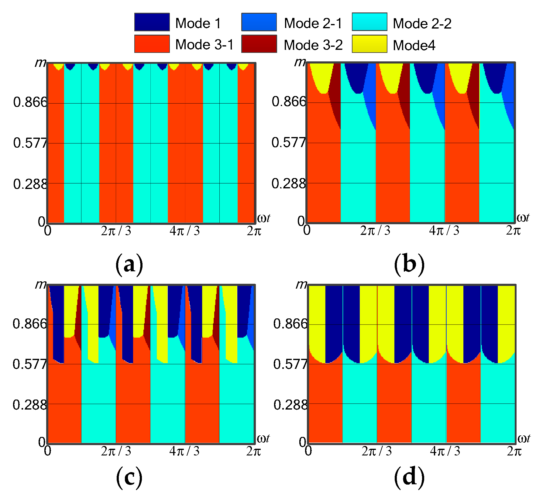
4. Selecting the Mode Based on the Switching Loss
It can be seen from Figure 3, Figure 4, Figure 5 and Figure 6 that there is at least one available mode in any condition of m and ωt, and there are even three available modes in some conditions of m and ωt, so an optimal available mode can be chosen. In this paper, the minimum switching loss is used as the selection criterion. The switching loss evaluation function for different modes can be expressed as:
where fk represents the switching action number of phase k.
Based on (16), the selected modes with several certain values of φ under the whole range of m and ωt are shown in Figure 7. While φ = 0, it is necessary to switch between modes 1, 2-2, 3-1 and 4 when m is greater than 1 and it is only necessary to switch between modes 2-2 and 3-1 when m is less than 1. While φ = π/2, it is necessary to switch between modes 2-2 and 3-1 when m is about less than 0.577 and it is necessary to switch between modes 1 and 4 when m is about greater than 0.577.
5. The Implementation of FRCVBPWM
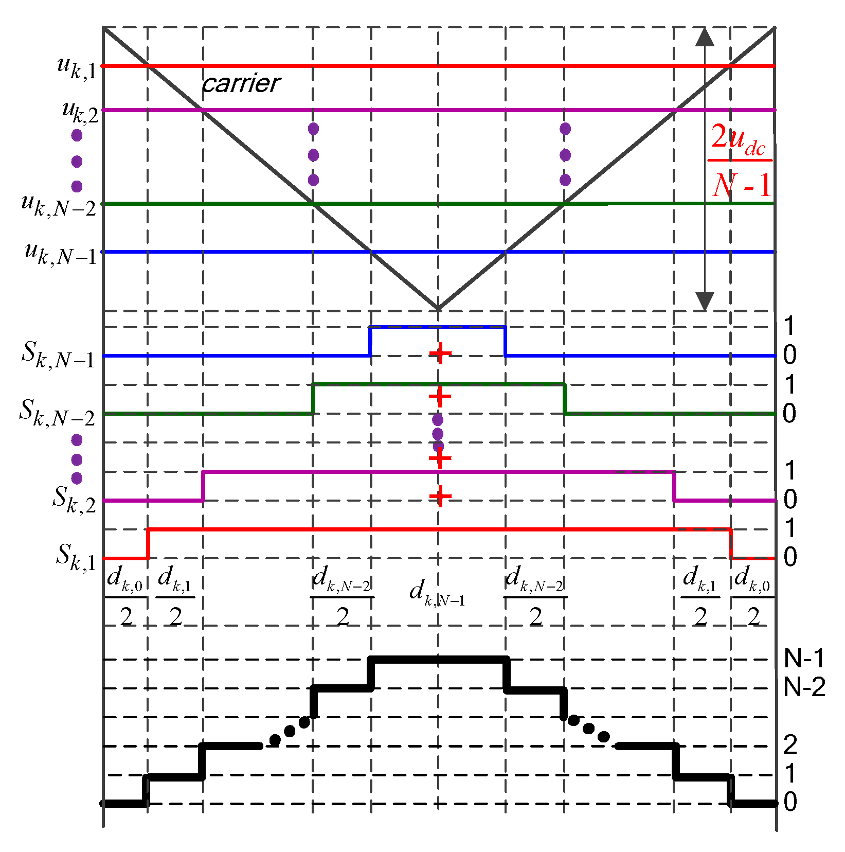
A carrier-based PWM method generates the PWM sequences by comparing the carrier with the modulation wave. This method is used for the implementation of FRCVBPWM because it can be easily carried out. For a multilevel inverter, multiple modulation waves are required, which can be obtained based on geometric relationships:
Multiple PWM sequences can be acquired by comparing a single carrier with multiple modulation waves; then, the final PWM sequence of the FRCVBPWM can be realized by adding the acquired multiple PWM sequences, as shown in Figure 8. The switching action number of FRCVBPWM and VSVPWM under different levels is shown in Table 3.
6. Switching Loss Analysis
For different modulation strategies, the conduction losses are generally considered to be equal and are not taken into account. Therefore, the loss analysis mainly focuses on switching losses. The average switching losses in a fundamental period can be calculated using the method proposed in [24], which is adopted here. When the phase current peaks are the same, the average switching losses of FRCVBPWM and VSVPWM with the variation of φ and m can be calculated, which are recorded as PSL_FCVB and PSL_VSV, respectively.
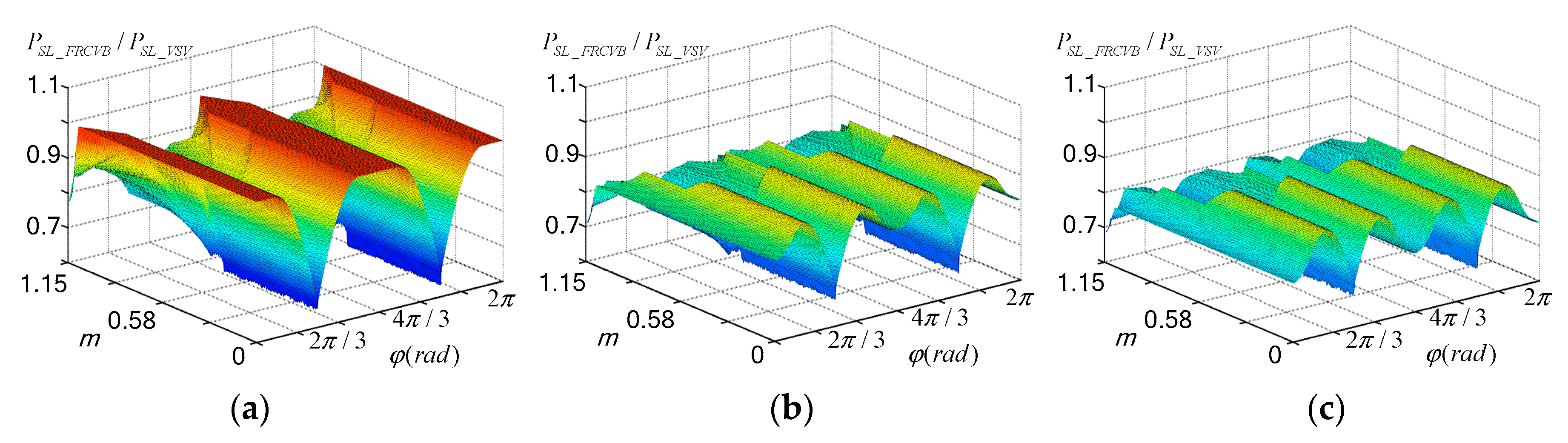
Figure 9 shows the ratios of PSL_FCVB to PSL_VSV for a DCMLI with different levels. It can be seen that in the operating range of the higher m and lower PF, the switching losses of FRCVBPWM are significantly lower than that of VSVPWM. In addition, the ratios of PSL_FCVB to PSL_VSV are reduced more obviously with the increase of levels.
7. Experimental Verification
A three-level DCMLI is built to verify the proposed FRCVBPWM. The DSP used as the main controller chip is Freescale’s MC56F84789, and the IGBT model used as the switching device is F3L300R07PE4. The experimental parameters are listed in Table 4.
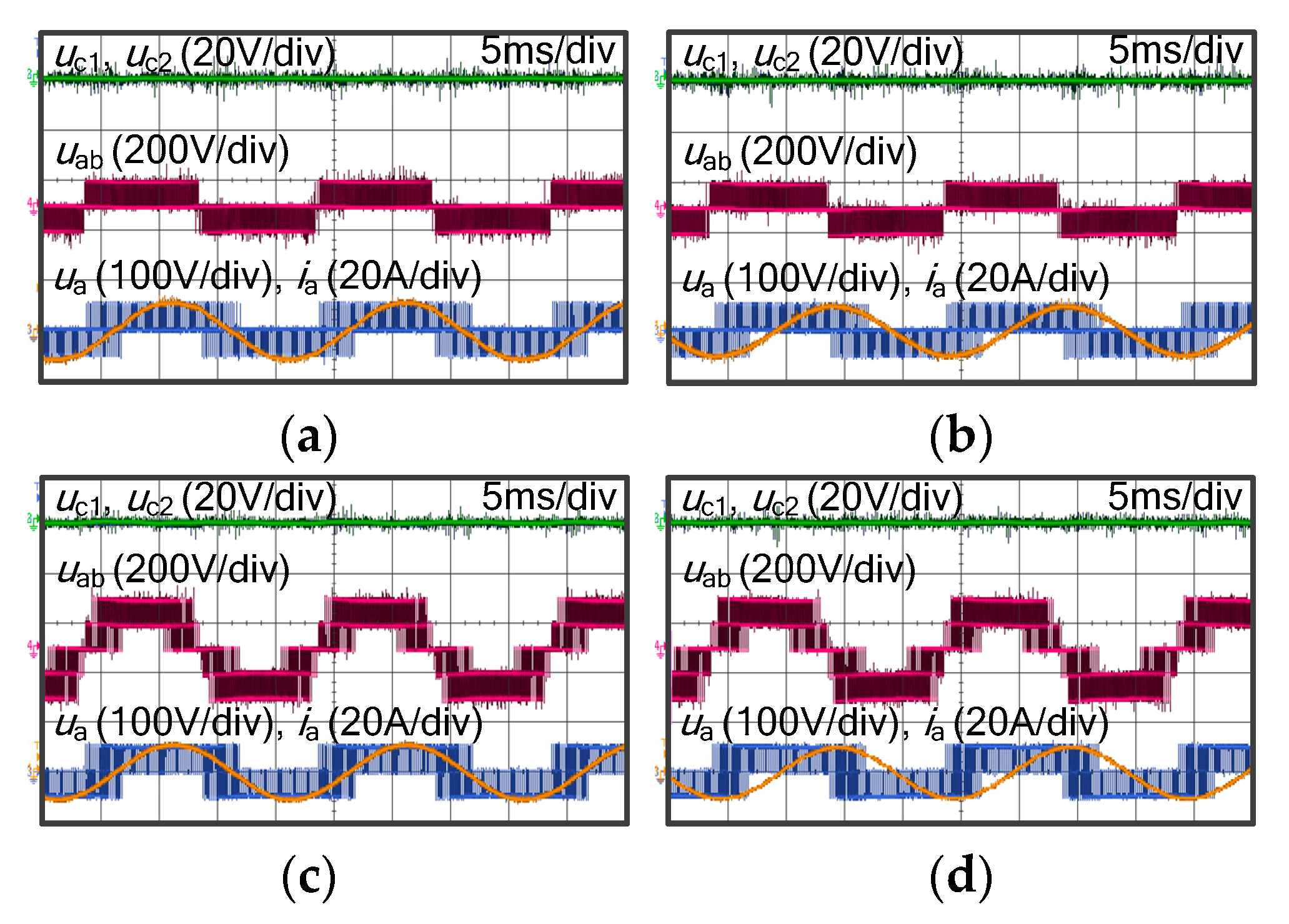
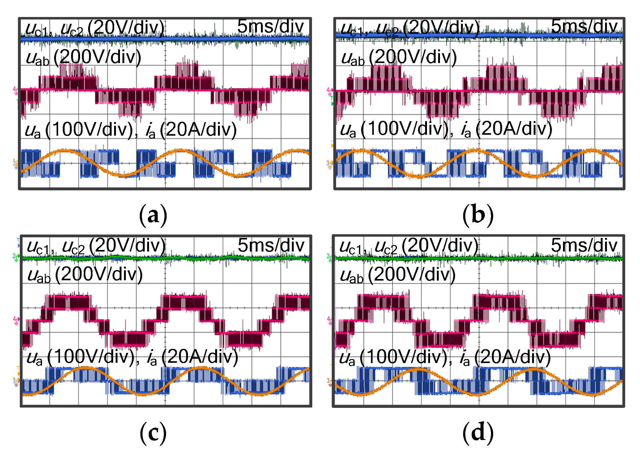
The steady-state experimental results under four conditions with different m and φ for FRCVBPWM and VSVPWM are shown in Figure 10 and Figure 11, respectively. The capacitor voltage can be controlled effectively under the two modulation strategies.
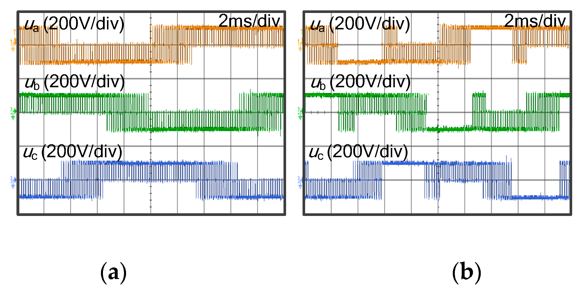
From the waveform of phase voltage ua shown in Figure 10, it can be seen that there is about one-third of an interval of a fundamental cycle in which it outputs levels 0, 1 and 2. It indicates that there are two switching actions during this interval, and there is one switching action during the other interval. From the waveform of phase voltage ua shown in Figure 11, it can be noted that there is a clamping interval in which the phase voltage ua is clamped to the positive or negative bus. Moreover, the interval with two switching actions is roughly equal to the clamping interval. Thus, each phase has one switching action on average, which reduces the switching losses of FRCVBPWM.
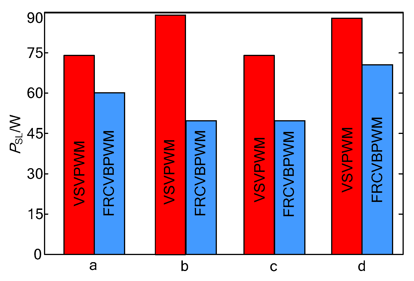
For FRCVBPWM and VSVPWM, the switching loss comparisons under four conditions are shown in Figure 12. When PF is higher, the switching loss difference between FRCVBPWM and VSVPWM is very small. When PF is lower, the switching losses of VSVPWM are significantly greater than that of FRCVBPWM.
When m = 0.3, the three-phase voltage for FRCVBPWM and VSVPWM in one fundamental period are shown in Figure 13. Under VSVPWM, the switching sequence of one phase is composed of levels 0, 1 and 2, and the other two phases are composed of two levels. Thus, there are in total four switching actions for the three phases in one switching cycle. Under FRCVBPWM, the switching sequence of one phase is composed of levels 0, 1 and 2, and one phase is composed of two levels, and one phase is clamped. Thus, there are in total three switching actions for the three phases in one switching cycle.
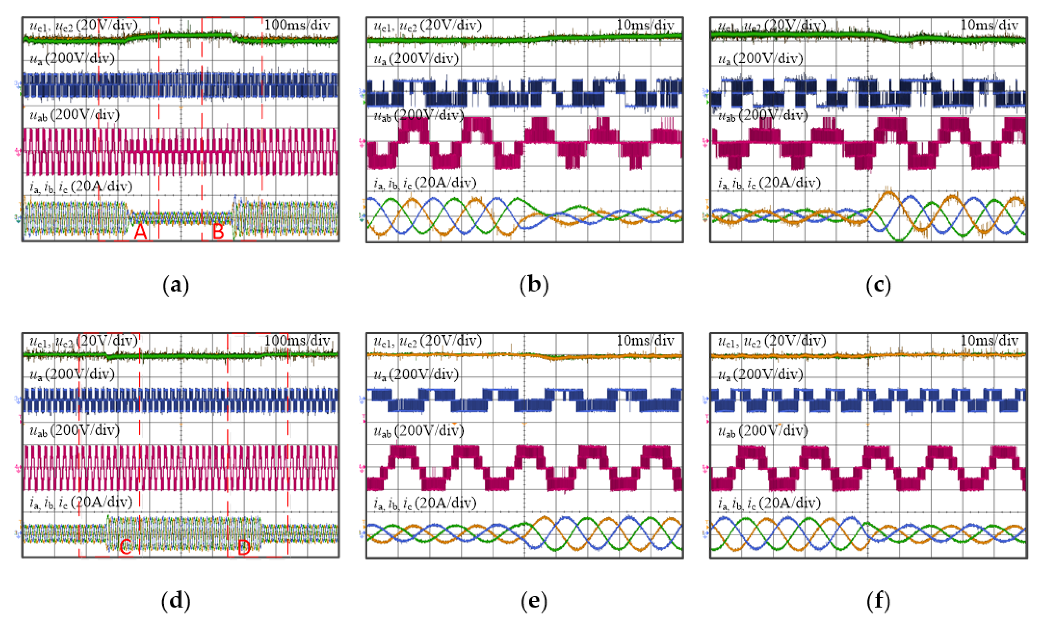
The dynamic experimental results of the proposed FRCVBPWM are presented in Figure 14, including a sudden change of m and load, respectively. From the dynamic experimental results, it can be seen that not only is DC offset, but also an AC ripple does not appear on the capacitor voltage. Therefore, the proposed FRCVBPWM has excellent capacitor voltage control performance both in steady state and dynamic process.
8. Conclusions
Because one phase is clamped, the switching action number of the proposed FRCVBPWM is reduced from 3N − 5 to 2N − 3 compared to VSVPWM for DCMLI applications, which greatly reduces switching loss. However, the full range capacitor voltage balance can be effectively achieved for FRCVBPWM, just like VSVPWM. Therefore, it can be concluded that the proposed FRCVBPWM has significant advantages in balancing capacitor voltage and reducing switching loss.
Author Contributions
Conceptualization, J.W. (Jinping Wang) and W.J.; methodology, J.W. (Jinping Wang); software, B.X.; validation, J.W. (Jinping Wang), J.W. (Juncan Wang) and Z.G.; formal analysis, J.W. (Juncan Wang) and Z.G.; investigation, J.W. (Jinping Wang); resources, J.W. (Juncan Wang) and W.J.; data curation, J.W. (Juncan Wang) and Z.G.; writing—original draft preparation, J.W. (Jinping Wang); writing—review and editing, J.W. (Juncan Wang); visualization, B.X.; supervision, W.J.; project administration, W.J.; funding acquisition, J.W. (Jinping Wang) and W.J. All authors have read and agreed to the published version of the manuscript.
Funding
This work was supported in part by the Fundamental Research Funds for the Central Universities of China under Grant JZ2019HGTB0074 and Grant PA2019GDPK0080, and in part by the Tianchang-HFUT Industrial Innovation Lead Key Funds Project under Grant JZ2019AHDS0002 and Grant JZ2020YDZJ0124.
Conflicts of Interest
The authors declare no conflict of interest.
References
- Rodríguez, J.; Lai, J.; Peng, F. Multilevel inverters: A survey of topologies, controls and applications. IEEE Trans. Ind. Electron. 2002, 49, 724–738. [Google Scholar] [CrossRef] [Green Version]
- Delmas, L.; Meynard, T.A.; Foch, H.; Gateau, G. Comparative study of multilevel topologies: NPC, multicell inverter and SMC with IGBT. In Proceedings of the IEEE 2002 28th Annual Conference of the Industrial Electronics Society, Sevilla, Spain, 5–8 November 2002; pp. 828–833. [Google Scholar]
- Renge, M.M.; Suryawanshi, H.M. Five-level diode clamped inverter to eliminate common mode voltage and reduce dv/dt in medium voltage rating induction motor drives. IEEE Trans. Power Electron. 2008, 23, 1598–1607. [Google Scholar] [CrossRef]
- Franquelo, L.G.; Rodriguez, J.; Leon, J.I.; Kouro, S.; Portillo, R.; Prats, M.A.M. The age of multilevel converters arrives. IEEE Trans. Ind. Electron. 2008, 2, 28–39. [Google Scholar] [CrossRef] [Green Version]
- Norambuena, M.; Kouro, S.; Dieckerhoff, S.; Rodriguez, J. Reduced multilevel converter: A novel multilevel converter with reduced active switches. IEEE Trans. Ind. Electron. Early Access 2018, 65, 3636–3645. [Google Scholar] [CrossRef]
- Lee, J.S.; Lee, K.B. A carrier-based PWM method for neutral-point ripple reduction of a 3-level inverter. In Proceedings of the 2014 IEEE Energy Conversion Congress and Exposition (ECCE), Pittsburgh, PA, USA, 14–18 September 2014; pp. 2095–2100. [Google Scholar]
- Shen, J.; Schroder, S.; Duro, B.; Roesner, R. A neutral-point balancing controller for a three-level inverter with full power-factor range and low distortion. IEEE Trans. Ind. Electron. 2013, 49, 138–148. [Google Scholar] [CrossRef]
- Gupta, K.; Khambadkone, A.M. A simple space vector PWM scheme to operate a three-level NPC inverter at high modulation index including over modulation region, with neutral point balancing. IEEE Trans. Ind. Electron. 2007, 43, 751–760. [Google Scholar]
- Dordevic, O.; Jones, M.; Levi, E. A comparison of carrier-based and space vector PWM techniques for three-level five-phase voltage source inverters. IEEE Trans. Ind. Inform. 2013, 9, 609–619. [Google Scholar] [CrossRef]
- McGrath, B.P.; Holmes, D.G.; Meynard, T. Reduced PWM harmonic distortion for multilevel inverters operating over a wide modulation range. IEEE Trans. Power Electron. 2006, 21, 941–949. [Google Scholar] [CrossRef]
- Chen, J.; He, Y.; Hasan, S.U.; Liu, J. A comprehensive study on equivalent modulation waveforms of the SVM sequence for three-level inverters. IEEE Trans. Power Electron. 2015, 30, 7149–7158. [Google Scholar] [CrossRef]
- Qin, J.; Saeedifard, M. Capacitor voltage balancing of a five-level diode-clamped converter based on a predictive current control strategy. In Proceedings of the 2011 Twenty-Sixth Annual IEEE Applied Power Electronics Conference and Exposition (APEC), Fort Worth, TX, USA, 6–11 March 2011; pp. 1656–1660. [Google Scholar]
- Rodriguez, J.; Pontt, J.; Silva, C.A.; Correa, P.; Lezana, P.; Cortes, P.; Ammann, U. Predictive current control of a voltage source inverter. IEEE Trans. Ind. Electron. 2007, 54, 495–503. [Google Scholar] [CrossRef]
- Busquets-Monge, S.; Alepuz, S.; Bordonau, J.; Peracaula, J. Voltage balancing control of diode-clamped multilevel converters with passive front-ends. IEEE Trans. Power Electron. 2008, 23, 1751–1758. [Google Scholar] [CrossRef]
- Saeedifard, M.; Iravani, R.; Pou, J. Analysis and control of DC capacitor voltage drift phenomenon of a passive front-end five level converter. IEEE Trans. Ind. Electron. 2007, 54, 3255–3266. [Google Scholar] [CrossRef]
- Lewicki, A.; Krzeminskiv, Z.; Abu-Rub, H. Space-Vector Pulsewidth modulation for three-level NPC converter with the neutral point voltage control. IEEE Trans. Ind. Electron. 2011, 58, 5076–5086. [Google Scholar] [CrossRef]
- Saeedifard, B.M.; Iravani, R.; Pou, J. Control and DC-capacitor voltage balancing of a space vector-modulated five-level STATCOM. IEEE Trans. Power Electron. 2009, 2, 203–215. [Google Scholar] [CrossRef]
- Hasegawa, K.; Akagi, H. A new DC-voltage-balancing circuit including a single coupled inductor for a five-level diode clamped PWM inverter. IEEE Trans. Ind. Electron. 2011, 47, 841–852. [Google Scholar] [CrossRef]
- Shu, Z.; He, X.; Wang, Z.; Qiu, D.; Jing, Y. Voltage balancing approaches for diode-clamped multilevel converters using auxiliary capacitor-based circuits. IEEE Trans. Power Electron. 2013, 28, 2111–2124. [Google Scholar] [CrossRef]
- Busquets-Monge, S.; Bordonau, J.; Boroyevich, D.; Somavilla, S. The nearest three virtual space vector PWM—A modulation for the comprehensive neutral-point balancing in the three-level NPC inverter. IEEE Power Electron. Lett. 2004, 2, 11–15. [Google Scholar] [CrossRef]
- Hu, C.; Yu, X.; Holmes, D.G.; Shen, W.; Wang, Q.; Luo, F.; Liu, N. An improved virtual space vector modulation scheme for three-level active neutral-point-clamped inverter. IEEE Trans. Power Electron. 2017, 32, 7419–7434. [Google Scholar] [CrossRef]
- Liu, P.; Duan, S.; Yao, C.; Chen, C. A double modulation wave CBPWM strategy providing neutral-point voltage oscillation elimination and CMV reduction for three-level NPC inverters. IEEE Trans. Ind. Electron. 2018, 65, 16–26. [Google Scholar] [CrossRef]
- Monge, S.B.; Alepuz, S.; Rocabert, J.; Bordonau, J. Pulse width modulations for the comprehensive capacitor voltage balance of n-Level three-leg diode-clamped converters. IEEE Trans. Power Electron. 2009, 24, 1364–1375. [Google Scholar] [CrossRef] [Green Version]
- Charumit, C.; Kinnares, V. Discontinuous SVPWM techniques of three-leg VSI-fed balanced two-phase loads for reduced switching losses and current ripple. IEEE Trans. Power Electron. 2015, 30, 2191–2204. [Google Scholar] [CrossRef]
Figure 1.
The topology of the diode-clamped multilevel inverter (DCMLI).

Figure 2.
The PWM sequences for the FRCVBPWM under different modes: (a) Mode 1, (b) Mode 2-1, (c) Mode 2-2, (d) Mode 3-1, (e) Mode 3-2, and (f) Mode 4.
Figure 2.
The PWM sequences for the FRCVBPWM under different modes: (a) Mode 1, (b) Mode 2-1, (c) Mode 2-2, (d) Mode 3-1, (e) Mode 3-2, and (f) Mode 4.

Figure 3.
The application area for different modes while φ = 0: (a) Mode 1, (b) Mode 2-1, (c) Mode 2-2, (d) Mode 3-1, (e) Mode 3-2, and (f) Mode 4.
Figure 3.
The application area for different modes while φ = 0: (a) Mode 1, (b) Mode 2-1, (c) Mode 2-2, (d) Mode 3-1, (e) Mode 3-2, and (f) Mode 4.

Figure 4.
The application areas for different modes while φ = π/6: (a) Mode 1, (b) Mode 2-1, (c) Mode 2-2, (d) Mode 3-1, (e) Mode 3-2, and (f) Mode 4.
Figure 4.
The application areas for different modes while φ = π/6: (a) Mode 1, (b) Mode 2-1, (c) Mode 2-2, (d) Mode 3-1, (e) Mode 3-2, and (f) Mode 4.

Figure 5.
The application areas for different modes while φ = π/3: (a) Mode 1, (b) Mode 2-1, (c) Mode 2-2, (d) Mode 3-1, (e) Mode 3-2, and (f) Mode 4.
Figure 5.
The application areas for different modes while φ = π/3: (a) Mode 1, (b) Mode 2-1, (c) Mode 2-2, (d) Mode 3-1, (e) Mode 3-2, and (f) Mode 4.

Figure 6.
The application areas for different modes while φ = π/2: (a) Mode 1, (b) Mode 2-1, (c) Mode 2-2, (d) Mode 3-1, (e) Mode 3-2, and (f) Mode 4.
Figure 6.
The application areas for different modes while φ = π/2: (a) Mode 1, (b) Mode 2-1, (c) Mode 2-2, (d) Mode 3-1, (e) Mode 3-2, and (f) Mode 4.

Figure 7.
The selected modes based on minimum switching loss under several certain values of φ: (a) φ = 0, (b) φ = π/6, (c) φ = π/3, and (d) φ = π/2.
Figure 7.
The selected modes based on minimum switching loss under several certain values of φ: (a) φ = 0, (b) φ = π/6, (c) φ = π/3, and (d) φ = π/2.

Figure 8.
Realization of FRCVBPWM based on the carrier-based PWM.

Figure 9.
The duty ratios of PSL_FRCVB to PSL_VSV under different levels: (a) three-level, (b) four-level, and (c) five-level.
Figure 9.
The duty ratios of PSL_FRCVB to PSL_VSV under different levels: (a) three-level, (b) four-level, and (c) five-level.

Figure 10.
Steady state experimental results of virtual space vector pulse width modulation (VSVPWM): (a) m = 0.3, φ = π/12, (b) m = 0.3, φ = 5π/12 (c) m = 0.9, φ = π/12 and (d) m = 0.9, φ = 5π/12.
Figure 10.
Steady state experimental results of virtual space vector pulse width modulation (VSVPWM): (a) m = 0.3, φ = π/12, (b) m = 0.3, φ = 5π/12 (c) m = 0.9, φ = π/12 and (d) m = 0.9, φ = 5π/12.

Figure 11.
Steady state experimental results of FRCVBPWM: (a) m = 0.3, φ = π/12, (b) m = 0.3, φ = 5π/12, (c) m = 0.9, φ = π/12, and (d) m = 0.9, φ = 5π/12.
Figure 11.
Steady state experimental results of FRCVBPWM: (a) m = 0.3, φ = π/12, (b) m = 0.3, φ = 5π/12, (c) m = 0.9, φ = π/12, and (d) m = 0.9, φ = 5π/12.


Figure 13.
The waveforms of three phases voltage for FRCVBPWM and VSVPWM: (a) VSVPWM, and (b) FRCVBPWM.
Figure 13.
The waveforms of three phases voltage for FRCVBPWM and VSVPWM: (a) VSVPWM, and (b) FRCVBPWM.

Figure 14.
Dynamic experimental results of FRCVBPWM: (a) a sudden change of m between 70.3 and 0.9, (b) partially enlarged waveforms of region A, (c) partially enlarged waveforms of region B, (d) a sudden change of load, (e) partially enlarged waveforms of region C, and (f) partially enlarged waveforms of region D.


Table 1.
The switching number under different modes of full range capacitor voltage balance PWM (FRCVBPWM).
Table 1.
The switching number under different modes of full range capacitor voltage balance PWM (FRCVBPWM).
| MAX_PB/MID_N − 1/MIN_N − 2 | MAX_PB/MIN_N − 1/MID_N − 2 | MIN_NB/MAX_N − 1/MID_N − 2 | MIN_NB/MID_N − 1/MAX_N − 2 | |
|---|---|---|---|---|
| umax | 0 | 0 | N − 1 | N − 2 |
| umid | N − 1 | N − 2 | N − 2 | N − 1 |
| umin | N − 2 | N − 1 | 0 | 0 |
Table 2.
All duty ratios under different modes of FRCVBPWM.
| Mode | Duty Ratio | Mode | Duty Ratio |
|---|---|---|---|
| Mode 1: MAX_PB/MID_N − 1/MIN_N − 2 | Mode 2-1: MAX_PB/MIN_N − 1/MID_N − 2 (The output sequence of the phase corresponding to umid is composed of levels 1... , N − 1) | ||
| Mode 2-2: MAX_PB/MIN_N − 1/MID_N − 2 (The output sequence of the phase corresponding to umid is composed of levels 0..., N − 2) | Mode 3-1: MIN_NB/MAX_N − 1/MID_N − 2 (The output sequence of the phase corresponding to umid is composed of levels 1..., N − 1) | ||
| Mode 3-2: MIN_NB/MAX_N − 1/MID_N − 2 (The output sequence of the phase corresponding to umid is composed of levels 0..., N − 2) | Mode 4: MIN_NB/MID_N − 1/MAX_N − 2 |
Remark: .
Table 3.
The switching action number of FRCVBPWM and VSVPWM.
| Three-Level | Five-Level | ...-Level | N-Level | |
|---|---|---|---|---|
| FRCVBPWM | 3 | 7 | ... | 2N − 3 |
| VSVPWM | 4 | 10 | ... | 3N − 5 |
Table 4.
Experimental parameters.
| Parameter | Value |
|---|---|
| DC side voltage | 200 V |
| Upper and lower capacitance values | 1000 μF |
| Load factor with high PF 1 (ZH1) | 2ejπ/12 Ω |
| Load factor with high PF 2 (ZH2) | 6ejπ/12 Ω |
| Load factor with low PF 1 (ZL1) | 2ej5π/12 Ω |
| Load factor with low PF 2 (ZL2) | 6ej5π/12 Ω |
| Fundamental frequency | 50 Hz |
© 2020 by the authors. Licensee MDPI, Basel, Switzerland. This article is an open access article distributed under the terms and conditions of the Creative Commons Attribution (CC BY) license (http://creativecommons.org/licenses/by/4.0/).
Share and Cite
MDPI and ACS Style
Wang, J.; Wang, J.; Xiao, B.; Gui, Z.; Jiang, W. Full Range Capacitor Voltage Balance PWM Strategy for Diode-Clamped Multilevel Inverter. Electronics 2020, 9, 1263. https://doi.org/10.3390/electronics9081263
AMA Style
Wang J, Wang J, Xiao B, Gui Z, Jiang W. Full Range Capacitor Voltage Balance PWM Strategy for Diode-Clamped Multilevel Inverter. Electronics. 2020; 9(8):1263. https://doi.org/10.3390/electronics9081263
Chicago/Turabian StyleWang, Jinping, Juncan Wang, Benxian Xiao, Zaiyi Gui, and Weidong Jiang. 2020. "Full Range Capacitor Voltage Balance PWM Strategy for Diode-Clamped Multilevel Inverter" Electronics 9, no. 8: 1263. https://doi.org/10.3390/electronics9081263
Note that from the first issue of 2016, this journal uses article numbers instead of page numbers. See further details here.