Flash Welding of Microcomposite Wires for Pulsed Power Applications


Vilnius Gediminas Technical University, Saulėtekio al. 11, LT-10223 Vilnius, Lithuania
*
Author to whom correspondence should be addressed.
Metals 2020, 10(8), 1053; https://doi.org/10.3390/met10081053
Submission received: 30 June 2020
/
Revised: 21 July 2020
/
Accepted: 29 July 2020
/
Published: 5 August 2020
Abstract
:This paper presents the experimental results of Cu-Nb wire joining upon applying flash welding technology. The present research is aimed at investigating the structure, electrical and mechanical properties of butt welding joints of Cu-Nb conductors, usable for coils of pulsed magnetic systems. The butt joint structure was found to be free of welding defects. The structure of the butt welded joint provides an insignificant increase in electrical resistance and sufficient ultimate strength and plasticity of the joint. The tensile strength of the welded sample reaches 630 MPa.
1. Introduction
Magnetic systems are quite simple in their construction and use low electrical power; therefore, they are popular in various fields of science and industry [1]. The key element of such magnetic systems is the inductor, of which the most popular type is multilayer wound. The materials of the conductors of such inductors must be very strong and have good electrical conductivity. Magnetic fields over 45 T can be generated only in the form of short pulses; therefore, the electrical wires must stand extreme impact load and cyclic heating. Therefore, new types of composite materials are used for winding; these include Cu-Nb, Cu-Ag, Cu-Al2O3, CuSS, Cu-Nb-Ti, Nb-Sn, Cu/C/S2 MC wires and others [2,3,4,5]. Cu-Nb microcomposite is presently considered to be one of the best types of modern conductor for pulsed power applications, due to its complete set of unique properties [6]. The ultimate tensile strength of this microcomposite conductor can reach 1.5 GPa; its yield strength can reach 1.0 GPa and Young’s modulus can reach 126 GPa when electrical conductivity is about 67–70% IACS [1,7,8]. This new composite conductor is used in different magnetic systems but also in levitation transport, high-voltage power lines, induction welding and industrial equipment for thermal treatment. Presently, the microcomposite wires have limited capability for deformation and the construction of inductors for high magnetic field equipment is multi-sectional; therefore, it needs many electrical contact connections [9,10].
In electrical engineering, wire and cable connections may be destructive (screw) or non-destructive (welded, soldered or pressed). Usually, access to all connections while operating magnetic systems is very limited. Therefore, contact connections must never be the weakest component of the system [11]. However, in practice, only screwed and soldered conductor connections are usually used, which do not demonstrate sufficient reliability and long service life in terms of impact loading and cyclic heating [12]: in comparison, welded joints are non-destructive and more reliable. The complexity of selection of welding technologies and parameters for joining of Cu-Nb microcomposites arises from the structure and production specificity of this microcomposite, as well as conditions of exploitation of pulsed magnets. The structure of Cu-Nb microcomposites consists of a copper matrix where very thin Nb threads are integrated as reinforcement [13,14,15,16]. The technology of Cu-Nb microcomposite wire production is similar to the process of multistage pressure or diffusion bonding, when the structure of the Cu-Nb microcomposite is obtained by multiple plastic deformations of both components. Traditional arc welding methods for connection of microcomposite wires cannot be used because of inevitable melting of the microcomposite structure, overheating of the joined wires and the loss of unique physical properties. Therefore, one of the important unsolved problems in the area of technologies based on high magnetic fields is the creation of a reliable, non-destructive connection of modern microcomposite conductors. This problem theoretically may be solved using special methods of welding, such as solid state welding or pressure welding.
2. The Peculiarities of Cu and Cu-Based Materials Resistance Welding
Butt resistance welding is often applied (including in the energy industry) for welding contact connections of conductors and electrical wires [17,18]. Although butt welding was widely used during the early industrial years, its applicability was limited because of the high current required [19]. Inherently, a majority of metals can be welded by applying this method. However, welding the contacts of copper and its alloys is complicated because of their high electrical and thermal conductivity, as well as the very narrow temperature range where the metal can be welded under pressure [20,21].
The weldability of copper alloys is somewhat better, as compared to technical copper, because their electrical conductivity and thermal conductivity are lower; however, not all copper alloys are highly weldable. Weldability is controlled by three factors: resistivity, thermal conductivity and melting temperature. These three properties can be combined into an equation [22], which will provide an indication of the ease of welding a metal:
where W—percentage weldability %; ρ0—electrical resistivity of material, µΩ cm; Tm—melting temperature of the metal, °C; Kt—relative thermal conductivity, with copper equal to 1.00 [23]. The physical properties of Cu/18 wt.% Nb conductors, investigated in present work, are listed in Table 1.
When weldability, W, is below 0.25, it is a poor rating. If W is between 0.25 and 0.75, weldability becomes fair. Between 0.75 and 2.0, weldability is good. Above 2.0, weldability is excellent. Copper and copper-based alloys have a very low weldability factor and are known to be very difficult to weld. For this reason, resistance welding may be applied in practice for copper and copper alloys having electrical conductivity higher than about 30% IACS [27,28,29,30,31]. The thermal and electrical conductivities of metals are proportional. The ratio of thermal to electrical conductivity illustrates the Wiedemann-Franz Law [32]:
where L—constant of proportionality is called the Lorenz number; W∙Ω∙°C−2; K—thermal conductivity, Wm−1∙°C−1; σ—electric conductivity, Ω−1∙m−1; T—temperature, °C
Upon taking into account the above-described regularities and the properties of the wire, the calculated weldability of Cu–18 wt.% Nb microcomposite wire is about 0.2. Hence, welding of this wire, like copper alloys, is complicated.
According to ISO 857 classification, resistance welding is classified as pressure welding in which sufficient outer force is applied to cause plastic deformation of both the faying surfaces, usually with heating of the faying surfaces by electrical current, in order to permit or to facilitate unifying [33]. This welding process is generally close to the process of producing Cu-Nb conductors. According to the degree of heating the edges to be unified, it is divided into flash welding (24–flash) and butt welding (25–butt) [34]. In butt resistance welding, the edges of details to be unified are heated up to a plastic state, whereas, in flash welding they are heated up till a layer of melted metal is formed.
In respect of the state of the metal in the welding area, both methods of resistance welding are considered solid-phase welding methods, although in some cases (especially in flash welding of large-diameter details), the welded coalescence is formed in the solid-liquid phase. The two methods are very similar to each other, differing only in that, in butt welding, the parts are brought together without voltage and under pressure, whereas in flash welding, the parts are bought together with voltage, so that, upon contact, a flash takes place [35,36].
Small diameter conductors and wires of copper and different metals are welded by butt welding and flash welding upon applying welding mode in solid state (duration of welding up to 1.5 s); for this purpose, condenser discharge welders may be used [35]. More welding modes in solid state with a shorter duration of welding (heating) are applicable when the thermal conductivity of the metals is higher. A welding mode in solid state ensures heat emission in a very narrow contact zone, when the influence of the thermal physical properties of the metal under welding on the heating and diffusion processes decreases considerably [36].
Butt welding was thought to produce weaker welds, as compared to flash welding. When the flash welding method is applied, a large volume of metal vapor is formed in the welding zone, which causes a reduction of the amount of oxygen contacting with the melted metal. So, in this case the welded seam is considerably neater, as compared to butt welding, if no protection of the welding zone is applied in any way [37]. In this case, the current applied to the workpieces produces a flashing or arcing across the interface of the two butting ends of the material. The flashing action increases to the point of bringing the material to a plastic state. This flashing action forms a heat-affected zone (HAZ) very similar to a butt weld. Smooth, clean workpiece surfaces are not as critical with this process as they are for butt welding, because the flashing action burns away irregularities at the weld surfaces [19]. The welding process is ended by a complete extrusion of the melted metal and oxides from the welded joint.
Three typical variants of flash welding exist—with continuous flashing, flashing under programmed voltage and flashing with heating. The second and the third variants are applicable for specimens of large diameters, so their application to those of small diameters is not reasonable [38]. These 3 variants of flash welding enable a wide variety of metallic materials to be joined and make possible the welding together of different metals and their alloys. In addition, they avoid the necessity to prepare the surfaces for joining and to ensure their close compression.
According to data from various sources, flash welding techniques produce very good results on copper and copper alloys upon applying welding equipment of considerably lower power [18,27,28,29,30]. However, butt flash welding requires a specific technique because of difficulties related to the necessity of holding a liquid layer on the edges under welding, as well as a need to preheat these edges to a certain depth prior to further upsetting. Rapid upsetting at minimum pressure is necessary as soon as the abutting faces are molten, because of the relatively low melting temperature and narrow plastic range of copper alloys [27,37]. In this case, the melting parameters depend on the thermal conductivity and the melting-point of the metal and are mostly predetermined by the rate of flashing.
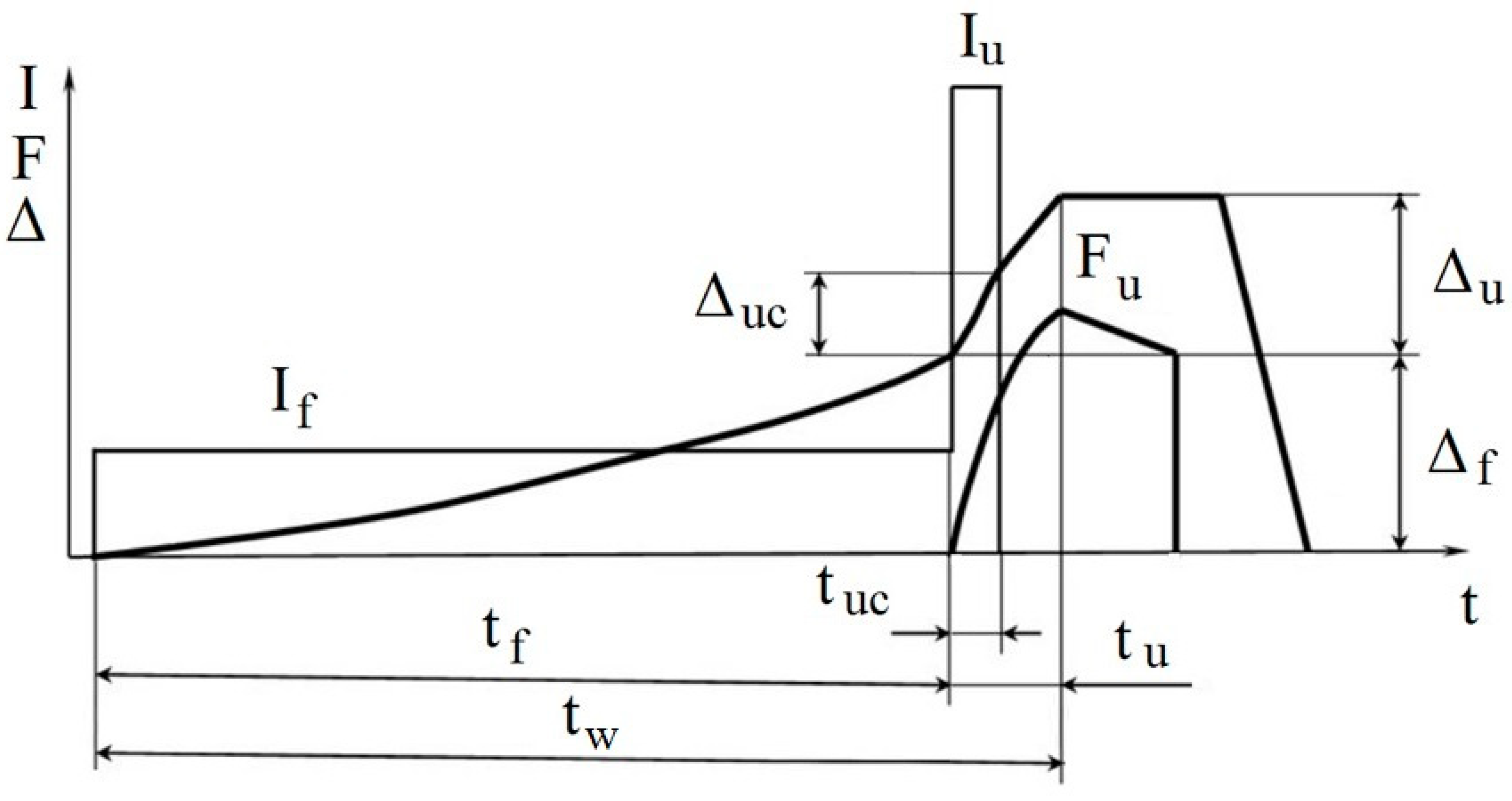
The rate and force of upsetting are also predetermined by the thermal conductivity of the metal and the activeness of its oxidation. The principal technological parameters of flash welding include—the flashing rate Vf; the flashing current If and the flashing current density jf; flashing time tf; the flashing allowance Δf; the upsetting current Iu and the upsetting current density ju; the upsetting allowance Δu and its rate Vu; the upsetting pressure pu; the upsetting force Fu; the upsetting time at current flowing tu; the base length l; and the voltage of idle mode of the machine U2x. The cyclogram of the flash welding process is presented in Figure 1.
The flashing current density for copper alloys is about 40–80 A∙mm−2, while the current density for flash welding ranges from 110 to 300 A∙mm−2 during the upsetting phase of welding [35,39]; current requirements during the flashing stage will be about 30–50% less than the upsetting current. Voltages vary from 2 V to 7 V at a low cross-sectional area and up to 20 V for the thicker sections [35]. For the best results, the lowest possible voltage should be used that is consistent with stable flashing. The flashing rate applicable for copper alloys ranges from 2 to 8 mm∙s−1 [40]. The concentered heating of the contact zone of wires of copper and copper alloys, high upsetting rates (125–250 mm∙s−1) and upsetting pressure (245–294 MPa) ensure that the metal does not lose its strength in the zone of the weld joint and distinguishes itself with good plastic and electric properties. Better results are obtained, if the copper wires are affected by electric current while upsetting [39,40,41].
The electrical and mechanical characteristics of the welding machine exert a significant influence on resistance welding processes. The continued development of microprocessor controls, AC and DC power supplies, advanced hydraulics and servo valves has improved both butt and flash welding processes. Early on, butt welding was limited to smaller machines of 5 to 100 KVA and single-phase AC, which is usable for joining small diameter wires and rods, such as coils for continuous line operations or wire frame applications [36].
Larger cross-sections of nonferrous material have been successfully welded with the use of three-phase DC butt welding machines. Such modern butt welding machines, equipped with a three-phase DC power supply & modern microprocessor control, provide balanced line demand, reduced primary current, narrower HAZ and minimized inductive losses.
Most flash welding machines use single-phase AC power supplies, but, as with the butt weld process, three-phase DC can also be used. The versatility of flash welding has increased with the addition of advanced hydraulics, servo valve combinations and electronic and microprocessor controls. These controls include feedback information to determine the velocity and acceleration of the two workpieces as they come together, current monitoring and flash voltage action. Modern flash welding machines with hydraulic operation can generate upset pressures of more than 200 t; this does not eliminate the flashing action but provides reduced primary current, high pressures with rapid acceleration, less material loss and a narrower HAZ. There is no significant difference in the weld quality of three-phase DC butt weld over-single phase AC flash welding [19,38].
The raised temperature makes flashing easier to start and maintain and helps to produce a well-distributed upsetting zone. Selection of preheat temperature depends upon the metal and size of the weld. A post heat treatment of welds may be added after the butt or flash welding is complete. A built-in function of post heat treatment of copper or its alloys may involve annealing, stress relieving and precipitation hardening, reducing the internal stresses and risk of cracking, while optimizing the mechanical properties [42].
The welding quality is improved considerably when the welding zone is protected with a shielding gas (argon, helium or a mixture of gases) or upon performing the welding in a vacuum (using a hood from which the air was pumped out). These methods are applicable for welding expensive metals prone to rapid oxidation, when it is important to reduce metal loss or avoid oxidation [35].
3. Methodology of Research
3.1. The Methodology of Calculation and Choosing a Regime of Flash Welding
The principle of resistance welding is Joule‘s heating law, where the heat Q is calculated according the following equation [20]:
where Q—the heat generated, J; Iw—the current passing through the metal joint, A; R—the complex resistivity of the metals and the contact interfaces, Ω; tw—the welding time, s.
The welding current is the most important parameter in resistance welding and determines the heat generation. The heat generation is directly proportional to the welding time. If the welding current is too low, simply increasing the welding time alone will not produce a sound weld. When the welding current is high enough, the size of the weld increases rapidly with an increase in the welding time. Very high current, however, will result in expulsions and welding defects [43].
The welding force influences the resistance welding process by its effect on the contact resistance at the contact area due to deformation of materials. The workpieces must be compressed with a certain force at the weld area to enable the flow of the electric current. If the welding force is too low, expulsion may occur immediately after starting the welding current due to the fact that the contact resistance is too high, resulting in rapid heat generation. If the welding force is very high, the contact area will be large, resulting in low current density and low contact resistance that will reduce heat generation and the weld size [44].
Nearly all material properties depend on temperature, which significantly influences the dynamics of the welding process. The resistivity of the material influences heat generation. The thermal conductivity and heat capacity influence heat transfer. In metals such as copper, with low resistivity and high thermal conductivity, little heat is generated even with high welding current and it is quickly transferred away. Therefore, Cu alloys are rather difficult to weld by means of resistance welding. When dissimilar metals are welded, more heat will be generated in the metal with higher resistivity.
Contact resistance at the weld interface is the most influential parameter related to materials. However, it has a highly dynamic interaction with the process parameters. All metals have rough surfaces in micro scale. When the welding force increases, the contact pressure increases, whereby the real contact area at the interface increases due to deformation of the rough surface asperities. Therefore, the contact resistance at the interface decreases, which reduces heat generation and the size of the weld nugget. On the metal surfaces, there are also oxides, water vapor, oil, dirt and other contaminants. When the temperature increases, some of the surface contaminants (especially water- and oil-based ones) will be burned off in the first couple of cycles and the metals will be softened at high temperatures. Thus, the contact resistance generally decreases with increasing temperature. Even though the contact resistance has the most significant influence only in the first couple of cycles, it has a decisive influence on the heat distribution, due to the initial heat generation and distribution [44].
The hardness of the material also influences contact resistance. Harder metals, with higher yield stress, will result in higher contact resistance at the same welding force, due to the rough surface asperities being more difficult to deform, resulting in a smaller real contact area [43].
Calculation of the parameters of flash welding is complicated because of the large number of variables, so experimental choosing the parameters of the welding is usually applied in practice. A preliminary approximation to the principal parameters of the welding process (if the properties of the material being welded are known) may be accomplished by applying simple empirical equations. In this case, the required base length, upon taking into account the flashing and upsetting allowances, is calculated according to the following equation [45]:
where Δu—the upsetting allowance, mm; Δf—the flashing allowance, mm; d—diameter of wire, mm.
The total allowance for flash welding is calculated according to the following equation [45]:
where d—diameter of wire, mm.
The flashing allowance is calculated according to the following equation [45]:
where l0—the total allowance for flash welding, mm.
The upsetting allowance at flowing of current is calculated according to the following equation [45]:
where Δu—the upsetting allowance, mm.
The upsetting allowance shall be found according to the following equation [45]:
where w—the total allowance for flash welding, mm.
The minimum upsetting force Fu may be calculated by taking into account the value of the specific pressure ρu, which depends on the welded metal [46]:
where S—the cross-section of the welded wire, m2; ρu—the specific upsetting pressure, Pa.
Specific pressure of copper is 10 × 106–15 × 106 Pa; copper alloys = 13 × 106–38 × 106 Pa; steels = 40 × 106–120 × 106 Pa [35,46].
The compression force shall be established from the dependence on the upset force [40,45]:
where k—the coefficient of sliding friction that depends on the properties of the clamps and the combination of welded metals, the structure of the clamps, the shapes of the details (equal to 1 for a copper-copper combination); Fu—the upsetting force, N.
The welding temperature at the end of the flash process is agreed to be as follows [40]:
where Tm—melting temperature, °C.
The flashing rate Vf is calculated according to the following equation, taking into account the chosen flashing time [45]:
where Δf—the flashing allowance, mm; Vf—the flashing rate, mm∙s−1.
The upsetting rate Vu is chosen in the range between 150 and 250 mm∙s−1 [45]. The upsetting time is calculated according to the following equation [45]:
where Δu—the upsetting allowance, mm; Vu—the upsetting rate, mm∙s−1.
The heat amount required for flashing is calculated according to the following equation [20]:
where L—latent heat of melting (metal melting heat), cal∙g−1; Vf—flashing rate, cm∙s−1; S—the area of the cross-section of the product, cm2; c—the specific thermal capacity of the metal, cal∙g−1∙°C−1; qf—the heat amount required for flashing, cals−1; γ—the density of the material, g∙cm−3.
The losses caused by heat runaway shall be calculated according to the following equation [20]:
where dT/dx—temperature gradient of joint, °C∙cm−1; S—the area of the cross-section of the product, cm2; λ—the thermal conductivity, cal∙cm−1∙s−1∙°C−1; qh—the losses caused by heat runaway, cal∙s−1.
The total heat amount to be emitted in the contact for melting the metal is calculated according to the following equation [20]:
The heat amount per second emitted at the chosen parameters of welding mode shall be calculated according to the following equation [20]:
where kc—coefficient, which takes into account the non-sinusoidal current waveform during flashing (equal to 0.7) [20]; If—electric current, A; R—total butt resistivity, Ω.
Flash welding may be carried out without the additional preheating, if the following condition is satisfied [20]:
The contact resistance Rf of the butt in the stage of metal flashing [20,45,47] is given by:
where Vf—flashing rate, cms−1; j—flashing current density, A∙mm−2; S—the area of cross-section of the product, cm2; Rf—the contact resistance of the butt, µΩ.
The contact resistance Rc of the welded metal wires at the end of the welding process is calculated according to the following equation [20,47]:
where Rc—the contact resistance between electrodes of the machine in the end of the process, Ω; l—the base length, cm; S—the cross-section of the welded details, cm2; ρt—the specific electric resistance of the metal at temperature T, Ω cm.
The dependence of the specific electrical resistance (resistivity) on temperature is described by the following equation [20]:
where ρt—the specific electric resistance of metal at temperature T, Ω∙cm; ρ0—the specific electric resistance of metal at the room temperature, Ω∙cm; α—the temperature coefficient of electric resistivity (for copper ~0.004) [20].
The total butt resistance R (upon neglecting the inductive component of the contour in the end of welding) shall be calculated according to the following equation [38]:
where Rf—the contact resistance of the butt, µΩ; R—the contact resistance between the electrodes of the machine at the end of the process, µΩ.
In a general case, if the electric current and the cross-section of the product being welded are known, the approximate flashing current density jf may be calculated according to the following equation [45]:
where jf—current density, Amm−2, S—the cross-section of the welded detail, mm2; If—electric current, A.
3.2. The Selection of Optimal Parameters of Flash Butt Welding
The parameters of the flash butt welding were calculated, taking into account the condition that duration of flashing should not exceed 1.5 s, the achieved temperature in the interface should be about 2100 °C, the duration of upsetting should not exceed 0.05 s, the rate of upsetting should be in the range from 125 to 250 mm∙s−1. The parameters that are agreed upon, taking into account the characteristics of the available contact machines, include the no-load voltage 3.4 V and the minimum duration of flashing 0.5 s. The results of calculating the welding parameters upon applying the empiric equations from Equations (9)–(29) are provided in Table 2, Table 3, Table 4 and Table 5.
In the case of flash welding, the total weld joint resistance (when conductors of small diameters are welded) mostly depends on the specific resistance of the metal Rc and the contact resistance of the interface (the sparking gap) Rf. In the case of flash welding, the contact resistance of the interface or, in other words, the resistance of the sparking gap is higher, as compared to other methods of resistance welding; in practice, its values vary between 100 and 2500 µΩ and it exists during the whole duration of the welding process [45]. In this case, when the welding currents range from 1500 to 2900 A, the values of resistance of the sparking gap Rf vary in the range 238–460 µΩ and do not overshoot these limits.
According to Table 5, only the two last regimes may be considered reasonable welding regimes, because the condition stated in Equation (23) is satisfied only in these cases. Upon applying other welding regimes, the heat amount per second emitted at the chosen welding parameters will be insufficient. According to preliminary calculations, the current density required for flash welding of this Cu-Nb conductor should achieve 270–290 A∙mm−2; such values correlate with the ranges of current recommended for copper alloys by various sources in the literature [20,35].
3.3. Materials and Welding Equipment, Welding Procedures and Methodology of Joints Testing
The commercially available microcomposite wire, Cu-Nb (82–18 wt.%) with 2.4 mm × 4.2 mm cross-sectional area was used for this research. The wire was manufactured using the ‘assembly-deformation’ method. The physical properties of the composite wire applied for calculating the parameters of welding regimes were established empirically by taking into account the properties of the pure metals (Cu and Nb, see Table 6) and their proportion in the composite [48,49,50,51,52].
where ɸ—the relative content of any phase; Z1, Z2—the value of a property of any phase; Z—the value of a property of the composite.
The mechanical and physical properties of this microcomposite wire are presented in Table 7 and Table 8 below:
The three-phase AC butt flash welding machine MKCCO (Chaika, Kiev, Ukraine) was used for butt welding of samples (Table 9). The temperature of joining area during welding was observed by a non-contact infrared pyrometer S-HW550 (Century Harvest Electronics Co., Limited, Shenzhen, China) with temperature range 50–2200 °C, accuracy ±2%, resolution 0.1 °C and response time 0.1 s, emissivity range 0.1–1.0 (for copper 0.7–0.8) [57].
The following welding parameters were used for flash welding of samples, taking into the account the results of welding regime calculations (Table 10).
Ar–0.03% NO (EN ISO 14175–Z–Ar+NO–0.03) gas was used as the shielding gas during all the experiments. The gas was supplied at a flow rate of 10 l∙min−1 through a Cu pipe of 10 mm internal diameter.
The evaluation of technical properties of the welded conductors’ joints were guided by standards GOST 10434, GOST 17,441 and EN ISO 5614-13 [59,60,61].
For the measurements of electrical resistivity, three fragments of Cu-Nb wire with butt joints were prepared. Each sample was 30 cm long. The experiments were carried out according to the methodology explained in the standards [56,57]. The electrical resistivity was measured using a U2810D Digital LCR (inductance, capacitance, resistance) Meter Tester (Changzhou Eucol Electronic Technology Co., Ltd, Changzhou, China). The Joule heating of the samples was observed using a Flir–E49001 (FLIR Systems, Wilsonville, OR, USA) thermal imaging camera. The samples were heated electrically with 200 A, using a welding rectifier VDU–305 (Velga, Vilnius, USSR). The temperature distribution was registered at the beginning of the experiment and after every 30 s.
The face of the welds was inspected visually by a 10× loupe and by higher magnification optical microscopy to detect imperfections. Additional non-destructive radiographic testing, which is not mandatory by EN 5614-13, was conducted in accordance with ISO 17636-1 and other standards [62]. GE ERESCO 42MF4 (General Electric, Boston, MA, USA) radiographic device, scanner Duerr NDT CR 35 NDT (Duerr NDT GmbH & Co. KG, Bietigheim-Bissingen, Germany), digital imaging software D–test viewer 9.3 (Duerr NDT GmbH & Co. KG, Bietigheim-Bissingen, Germany) were used for non-destructive testing. The selected welds were cross-sectioned to assess the weld profile. The microstructural analysis of the obtained welded joints was performed by following the EN ISO 17,639 requirements [63]. The microstructure of the joint was analyzed using scanning electron microscopy (SEM) and optical microscopy. For the microscopic investigation, the samples were prepared by abrasive grinding and diamond polishing and subsequently etched, using a solution of 8 g CuCl2 and 100 ml NH3 (25%). A SEM JEOL JSM–7600 (JEOL Ltd., Tokyo, Japan) equipped with an energy dispersive spectrometer (EDS) Oxford INCA Energy X–Max20 (Oxford Instruments plc, Abingdon, Oxfordshire, UK) for chemical microanalysis and an optical microscope Nikon MA–200 (Nikon Corporation, Tokyo, Japan) with a digital camera were used.
The mechanical properties of the samples were determined in accordance with standards GOST 6996 and ISO 4136 [64,65]. The static and dynamic tests were conducted. The most important mechanical properties (Young’s modulus, yield and tensile strength) of the samples with welded joints were determined via static tensile and bending testing. Three samples with welded butt joints, each 30 cm in length, were tested. The universal press TIRAtest 2300 (TIRA, Schalkau, Germany), with Catman–Express software (version 5.1, HBM, Germany) and dynamometer up to 20 kN were used; limit for load measurement error—±1.0%.
Nowadays, Young’s modulus can be determined and by dynamic tests (ultrasound and resonant vibration), which are more precise and versatile since they use very small strains, lower than the elastic limit and therefore are completely non-destructive and allow repeated testing of the same sample. To obtain the Young’s modulus, flexural vibration tests were conducted according to the following procedures. For the applied flexural vibration (fixed-free end) scheme, the Young’s modulus of material is expressed by the following equation [66]:
where h—thickness of rectangular specimen, mm; fn—natural frequency of vibration, Hz; L—length of beam, mm; ρ—mass density of material; kn—dimensionless coefficients for calculating the frequencies of the cantilever beam (Table 11).
The length of beam for dynamic tests was 90 mm. The average mass density of Cu-Nb wire was defined experimentally by dividing the mass of the object by its volume. The electronic analytical balance Kern ABP-200-4M (Kern & Sohn, Balingen, Germany) for weighing up to 200 g maximum with 0.1 mg resolution was used to perform density determination experiments. The theoretical density of the composite was determined according to Equation (25). The difference between measured (8.814 g∙cm−3) and theoretical mass density (8.889 g∙cm−3) of Cu-Nb wire did not exceed 1.0%. Therefore, the value of the theoretical mass density was used for calculation of Young’s modulus.
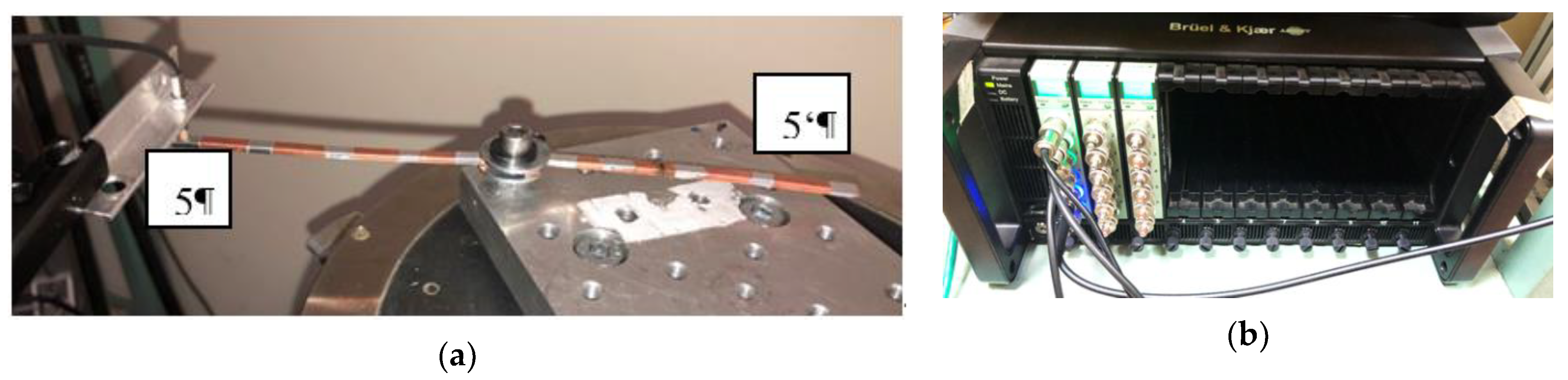
The bending vibration test was performed on a test table (Figure 2a), which isolated the system from environment noise and vibration. The “Brüel & Kjær” equipment for vibration measurement included:
- Portable equipment 3660-D (Brüel & Kjær, Nærum, Denmark) for processing, storage and handling of measurement results (Figure 2b);
- Personal computer DELL;
- Non-contact inductive position measurement sensors U20B and U3B (Lion precision, Oakdale, CA, USA) with amplifiers and an opacity source;
- Excitation vibrator 4810 (HP, Palo Alto, CA, USA) with amplifier and frequency generator.
Each specimen was prepared for detection of vibration at 5 different points, by sticking very thin aluminum foil to it. The two test specimens were hold tightly at their ends with the M6 screw (Figure 2a). The displacement of every point was detected by the small displacement sensor, U3B. Another much larger sensor, U20B, was used for detection of stable ground level and the vibrations of the whole system, including the test table.
Two types of dynamic test were performed: exciting the sample in a range of frequencies and an impact test. For the first method, the specimen was excited in a vibration mode at a frequency range between 50 and 1000 Hz with sweep rate 500 Hz/s. When exciting each point, the signal of swept sine was repeated several times and the frequency response was monitored.
For the impact method, the specimen was excited by hitting with a hammer at the free end to avoid resonance of the system and the sensor and get correct values of the natural frequencies. After the impact, the specimen freely vibrates vertically at its modes of vibration and all vibrations undergo a gradual decrease of amplitude with time. This impact method can be useful to predict only the first few resonant modes without exciting at the higher frequencies. As presented in previous studies [67,68,69], the most accurate values of calculated Young’s modulus are received from the first resonant modes; therefore, there is no need to try to measure the highest of them.
In both experiments, the signals of both sensors, after processing by portable equipment 3660-D, were sent to the PC, where the displacement of each point was plotted.
4. Experimental Results and Discussion
The correctness of the choice of welding parameters was assessed by measuring the achieved maximum heating temperature of the welded joint through a contactless method. At the end of welding, the maximum heating temperature was 2015 °C, that is, it conformed to the recommended range (temperatures from 0.7–0.75 Tm. to the melting point Tm [45]) and differed from the one used for calculation of welding regimes by about 4% only.
The general criteria for the quality of the welds are weld geometry, mechanical properties of the joint, quantity and size of internal and surface defects and weld microstructure. The welding quality was determined by radiographic non-destructive testing. No unacceptable internal welding defects (cracks, porosity, inclusions or other discontinuities) were observed from the digital X-ray images.
4.1. Results of Analysis of Microstructure of Welded Joints
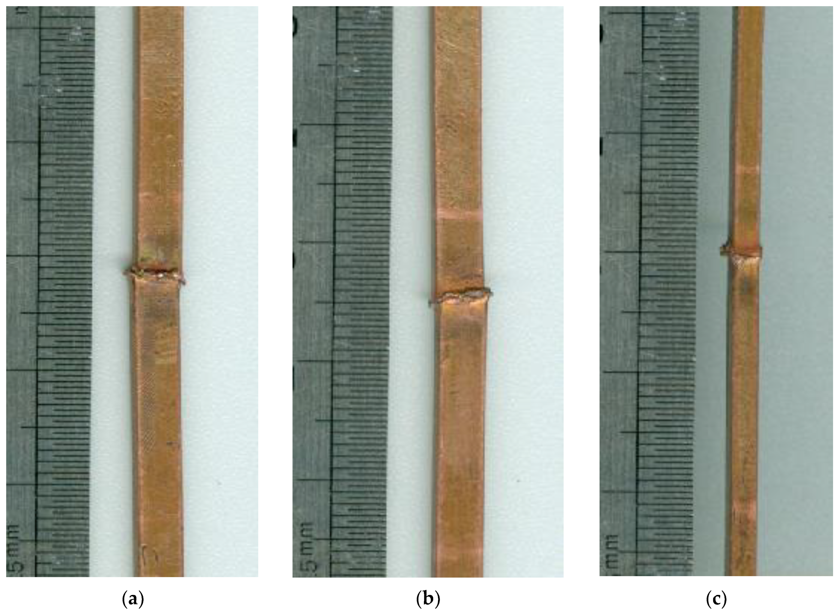
General views of the butt welds are shown in Figure 3. The microstructure and shape of the butt welds can be observed from the cross-section of joints. It can be seen from Figure 3 and Figure 4 that weld joints were formed by flash welding without lack of penetration, cracks, large misalignment or other discontinuity at the interface. The bonding line and edges of the Cu-Nb wire can be clearly identified from the view; however, the edges were joined completely and the welded joint was formed without any unacceptable discontinuities.
The main parameters defining the dimensions of the cross–section of the resistance welding joint are the width of partially melted and mechanically upset region. It is recommended that the width of this partially melted or deformed region should not exceed the value calculated according to the following equation [70]:
where d—the cross-section of the detail, mm.
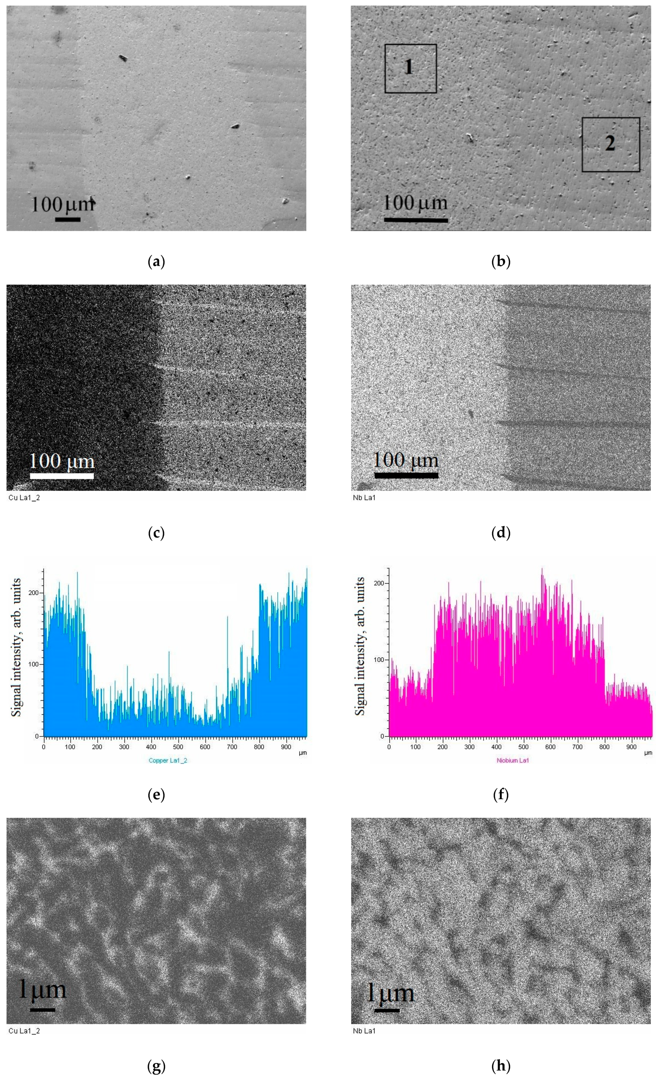
In this case, the recommended width of the mechanically upset region is ~1.4 mm. As can be seen from the cross–section view of the butt weld (Figure 3 and Figure 4a,b), no significant thickenings of the cross-section in the zone weld joint or deformations of the conductor caused by metal upsetting were practically observed in this case. On the joint, only a layer of melted metal extruded in the stage of upsetting of the wires (typical for this technology) is visible. The microstructure of obtained weld differs from that of the initial conductors (Figure 4a,b), indicating that the weld was formed due to the melting of the Cu-Nb conductor here. The melted area (weld) showed uniform microstructure and composition across the whole cross-section.
The width of the melted area achieves 0.65 mm (Figure 4a). The melted area of the joint consists mainly of copper (~29 wt.%) and niobium (~65 wt.%) (Table 12, region 1). The amount of other elements (C, O and Si appeared in the composition as a residues of cross-section preparation with SiC abrasive and surface oxidation/gas absorption at air) is ~7 wt.% (Table 12). After elimination of these elements, the concentrations of copper and niobium in melted zone were ~29 wt.% and ~71 wt.%, respectively.
As can be seen from Figure 4c–f, the procedure of flash welding ensures quite even distribution of Cu and Nb elements in the whole area of melting; however, their proportion differs from the chemical composition of the initial Cu-Nb wire (see Table 12, region 2). Nb concentration is up to 3.6 times higher–this fact attests that in the stage of upsetting, copper was mostly extruded from the zone of the joint, because of its higher yield and lower melting point.
As can be seen from elemental maps for Cu and Nb (Figure 4g,h), the microstructure of the melted area is composed of two phases, which, according to Cu-Nb phase diagram, may be identified as Cu-rich and Nb-rich terminal solid solutions. Because Cu and Nb have a negligibly low mutual solubility in the solid state, the Cu-rich and Nb-rich terminal solid solutions-based mechanical mixture is typical for the microstructure of Cu-Nb alloys. As in this case, the phases appeared to be quite dispersive (up to a few micrometers) and Nb concentration is increased, as compared to the composition of Cu-Nb wire; therefore, this may contribute to the good strength of the weld.
4.2. Results of Testing of Electrical Properties of Welded Joints
The electrical properties of the samples with a welded joint and the conductor without joint were compared by measuring the difference in their electrical resistivity. The conductor of 30 cm length had an electrical resistivity of 0.01 Ω at room temperature. A slight increase in resistivity was obtained in conductors with resistance welding joints. The samples with weld joints of the same length had an electrical resistivity of 0.011 Ω. The difference in electrical resistivity was not significant (1.1 times) and it did not exceed the standard recommended limit; the maximum difference in electrical resistivity between conductor and samples with welded joints should not reach 1.5 times [59,60].
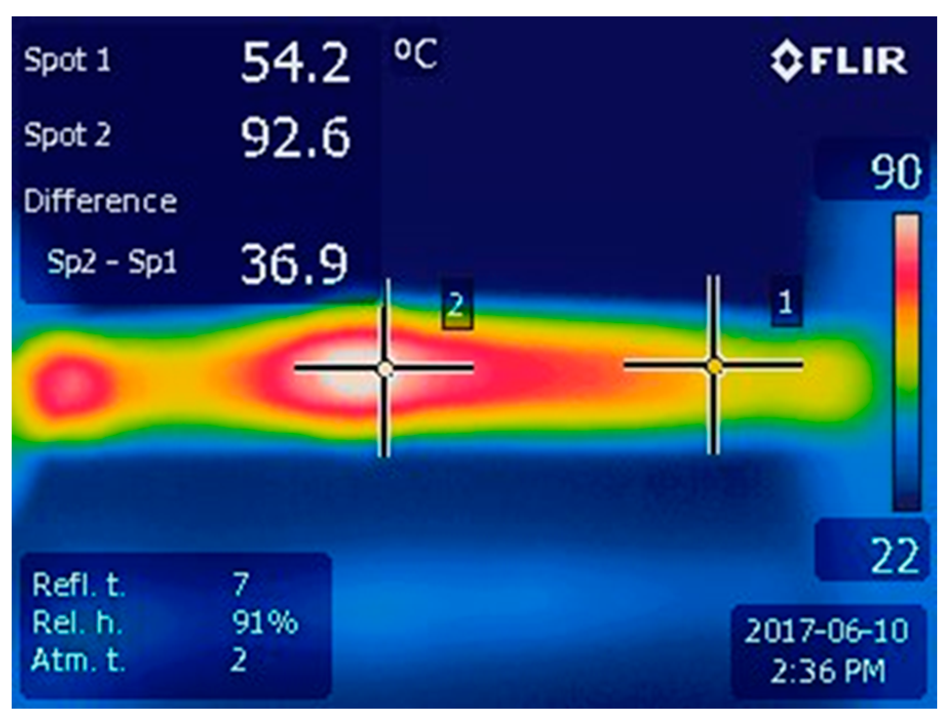
Heating of the samples with the welded joint during electrical current flows was registered using a thermal imaging camera. The temperature distributions at the beginning of this experiment and after 3 minutes of heating are presented in Figure 5. The temperature differences in the resistivity welding joints and conductor when electrical current flowed did not exceed the recommended value of 95 °C [59,60].
4.3. Results of Testing of Mechanical Properties of Welded Joints
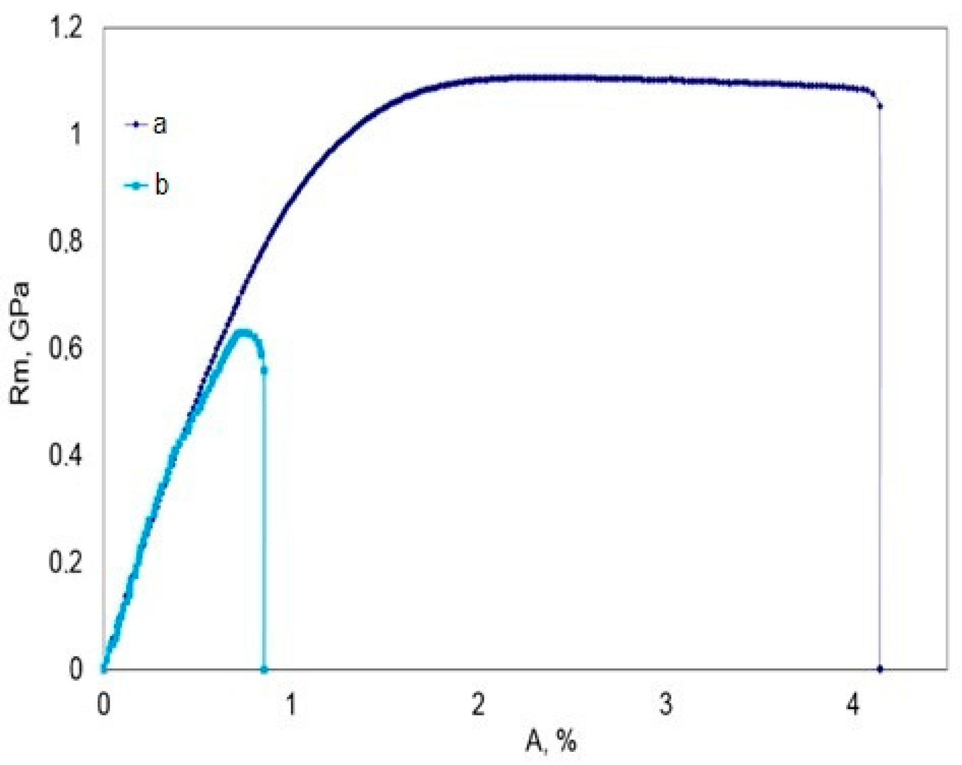
The tensile testing of samples with welded joints shows that all specimens break through the weld area. According to the Kurnakov rule [71,72], the minimum tensile strength of a Cu-65Nb (wt.%) weld could be ~454 MPa. The measured tensile strength of the sample with welded joint is about 1.4 times higher than that calculated for the Cu-65Nb (wt.%) binary metal system, obtained after casting. However, flash welding joints have lower ductility than the initial microcomposite wire.
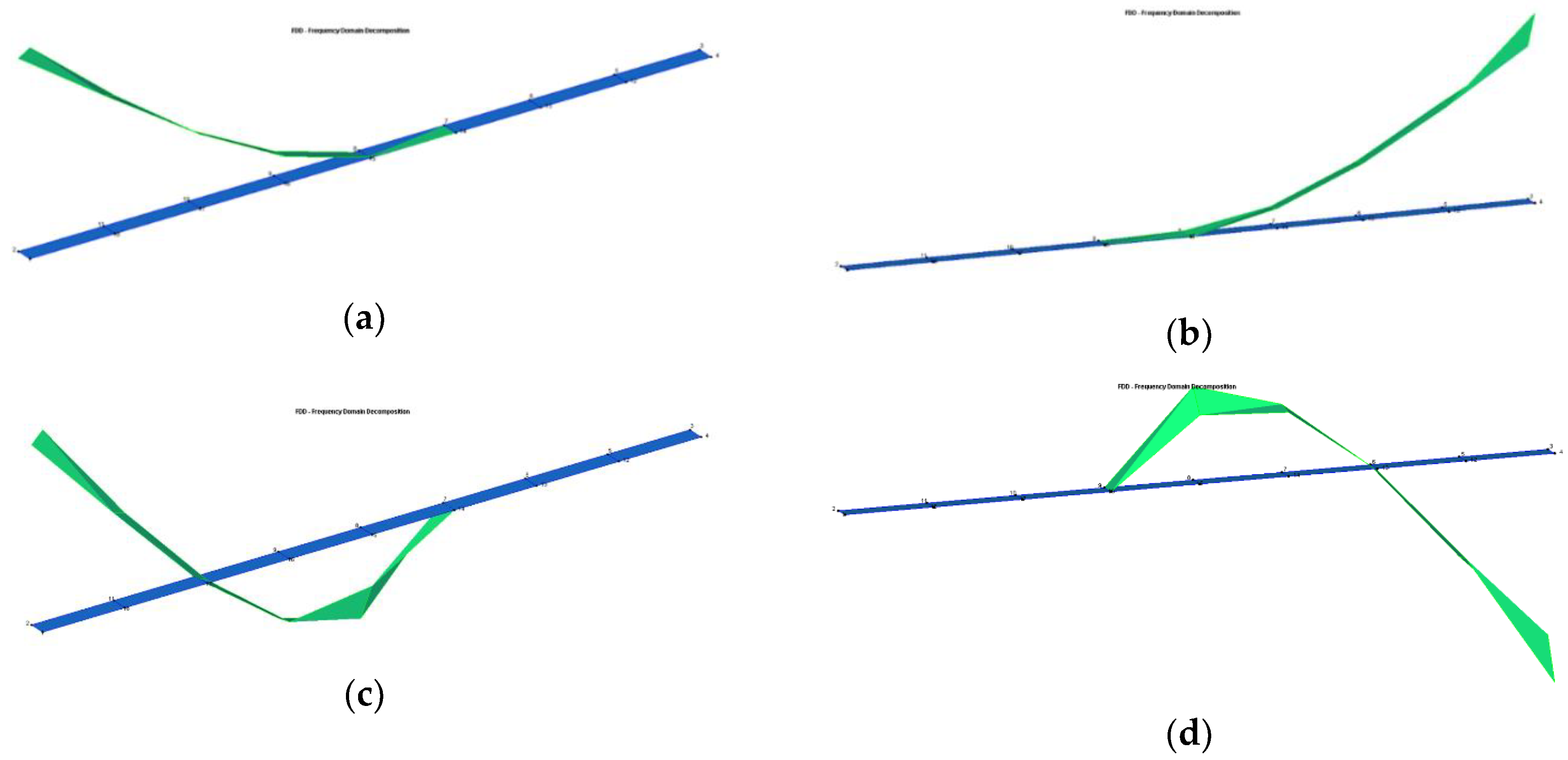
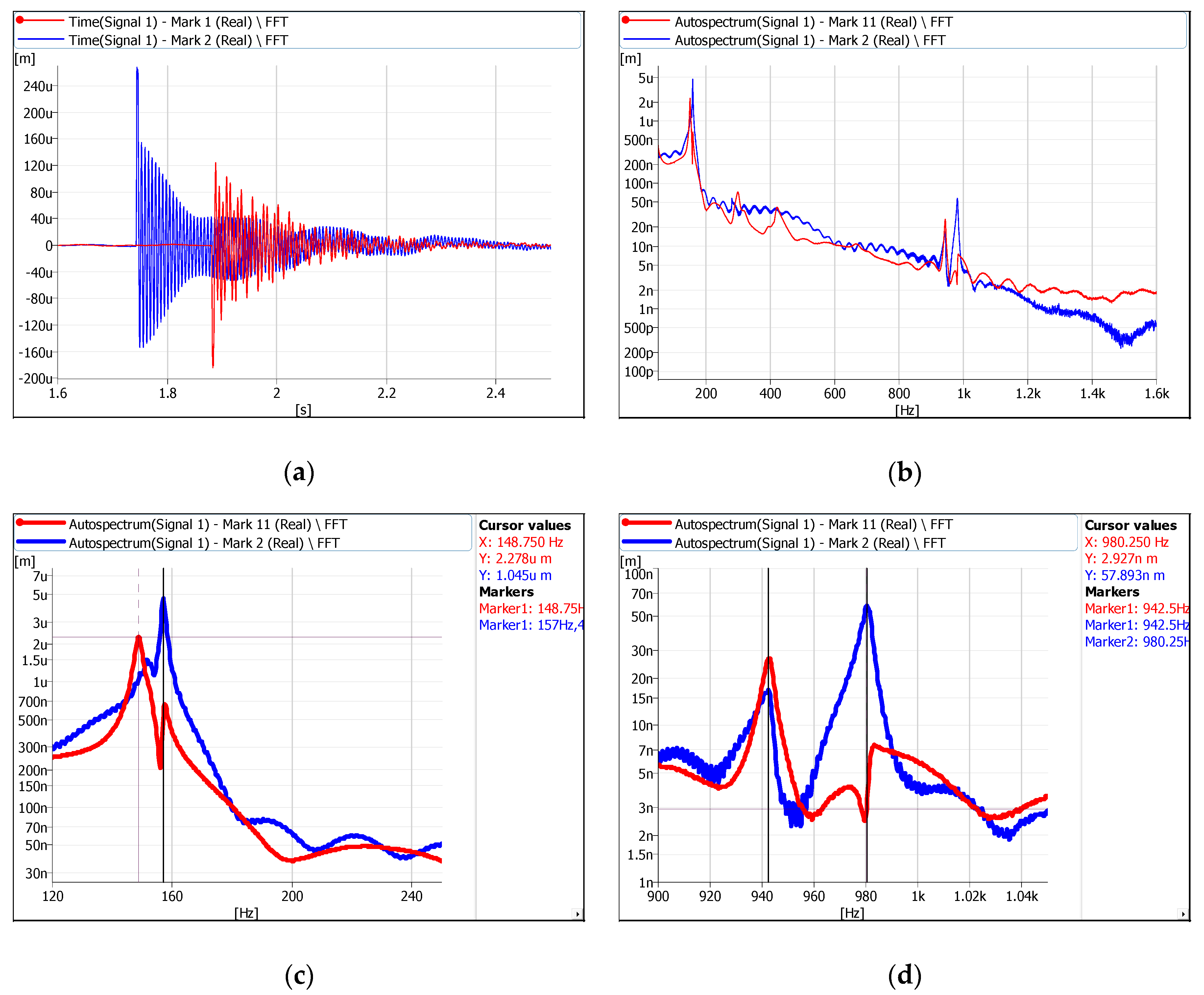
The minimal tensile load, which flash welded joint has withstood during three tests, was ~6300 N ± 1% (Figure 6). Accordingly, the minimal tensile stress in the area of the fracture reached 630.0 ± 6.3 MPa, which is adequate to ~56% of the tensile strength of the initial microcomposite wire (Figure 6). The percentage elongation of the sample of the connection after fracture was 0.9%. This is about 21.4% of the percentage elongation of the microcomposite wire. The tensile and bending testing of samples shows that the Young’s modulus of samples with and without welded joint is very similar. After the execution of dynamic tests, resonant frequencies were found (Table 13 and Table 14, Figure 7 and Figure 8).
The two first resonant modes were identified by applying experimental modal analysis are presented in Figure 7. The automatically detected resonant frequency of the first and second bending modes of the samples was used for calculation of Young‘s modulus. The Young’s modulus of the Cu-Nb wire established by the resonant frequency method did not exceed 95.949 GPa (Table 14). The values of Young’s modulus determined according to Equation (26) after dynamic testing of the Cu-Nb wire samples with and without welded joints were very similar. The difference between the Young’s modulus established by static (bending and tensile testing) and dynamic (resonant frequency) methods did not exceed 3.5%. The testing of specimens shows that the Young’s modulus of this composite material is constant and not affected by changes in the measuring method (Table 15).
5. Conclusions
In the present paper, microstructure, electrical and mechanical properties of Cu-Nb wire welded joint obtained upon applying flash welding technology were investigated. Several conclusions may be drawn based on the experimental results obtained.
- According to the microstructural analysis, the joint was formed due to the melting of Cu-Nb conductors in their contact zone. More ductile copper, having lower melting point, was partially extruded from the contact zone, resulting in an increase of Nb to Cu ratio in melted zone of the joint (~29 wt.% Cu and ~71 wt.% Nb), as compared with initial conductor. The melted area (weld) showed fine uniform microstructure composed of two phases–Cu-rich and Nb-rich terminal solid solutions.
- The obtained flash welded joints of Cu-Nb microcomposite have high tensile strength, which minimum obtained value reaches ~630 MPa, adequate to ~56% of the tensile strength of the initial microcomposite wire.
- The obtained structure of joint provides an insignificant increase in electrical resistivity (1.1 times higher than that of the initial conductor), sufficient ductility of the joint (about 21.4% of the percentage elongation of the microcomposite wire) and has negligible effect on Young’s modulus change.
Thus, flash welding technology, in principle, is applicable to electrical contact connections with Cu-Nb microcomposite wire. The flash welded joints are suitable for use in solenoid terminal connections with external electrical circuits that are not directly exposed to high magnetic or tensile forces that are generated inside a solenoid of a pulsed magnet system.
Author Contributions
Methodology, N.V.; investigation, N.V.; writing—original draft preparation, N.V.; investigation, O.Č.; data curation, O.Č.; visualization J.Š.; writing—review and editing, A.K.; supervision, A.K. All authors have read and agreed to the published version of the manuscript.
Funding
This research received no external funding.
Acknowledgments
The author team is grateful for all effort and support from the Joint-stock company, Relema (Lithuania) and, particularly, Atashes Chatajan for collaboration, handling of flash welding equipment, preparation of welded specimens and consulting.
Conflicts of Interest
The authors declare no conflict of interest.
References
- Herlach, F.; Miura, N. High Magnetic Fields. Magnet Technology and Experimental Techniques; Science and Technology; Imperial College Press: London, UK, 2003; Volume 1, p. 336. [Google Scholar]
- Shneerson, G.A.; Dolotenko, M.I.; Krivosheev, S.I. Strong and Superstrong Pulsed Magnetic Fields Generation. De Gruyter Studies in Mathematical Physics; De Gruyter: Berlin, Germany, 2006; pp. 147–178. [Google Scholar]
- Han, K.; Embury, J.D.; Sims, J.R.; Campbell, L.J.; Schneider-Muntau, H.J.; Pantsyrnyi, V.I.; Shikov, A.; Nikitin, A.; Vorobieva, A. The Fabrication, Properties and Microstructure of Cu-Ag and Cu-Nb Composite Conductors. Mater. Sci. Eng. 1999, 267, 99–114. [Google Scholar] [CrossRef]
- Brandao, L.; Han, K.; Embury, J.D.; Walsh, R.; Toplosky, V.; Van Sciver, S. Development of High Strength Pure Cooper Wires by Cryogenic Deformation for Magnet. Appl. IEEE Trans. Appl. Supercond. 2000, 10, 1282–1287. [Google Scholar]
- Gershman, I.S.; Gershman, E.I.; Peretyagin, P.Y. Composite Nanomaterials Based on Copper to Replace Silver in Electrical Contacts. Mech. Ind. 2016, 17, 708. [Google Scholar] [CrossRef] [Green Version]
- Bykov, A.A.; Popkov, S.I.; Parshin, A.M.; Krasikov, A.A. Pulsed Solenoid with Nanostructured Cu-Nb Wire Winding. J. Surf. Investig. X-Ray Synchrotron Neutron Tech. 2015, 9, 111–115. [Google Scholar] [CrossRef]
- Rossel, K.; Herlach, F.; Vanacken, J.; Van Humbeeck, J. Multi-Composite Wire for High Performance. Pulsed Magnets. IEEE Trans. Appl. Supercond. 2004, 14, 1149–1152. [Google Scholar] [CrossRef]
- Raabea, D.; Hangen, U. Investigation of Structurally Less-Ordered Areas in the Nb Filaments of a Heavily Cold-Rolled Cu-20 wt. % Nb in Situ Composite. J. Mater. Res. 1995, 10, 3050–3061. [Google Scholar] [CrossRef]
- Blumber, L.; Hasizume, H.; Ito, S.; Minervini, J.; Yanagi, N. Status of High Temperature Superconducting Magnet Development; RSFC/JA-10-45 Report; National Institute for Fusion Science: Toki City, Japan, 2010; p. 20. [Google Scholar]
- Jones, H.; Van Cleemput, M.; Hickman, A.L.; Ryan, D.T.; Saleh, P.M. Progress in High-Field Pulsed Magnets and Conductor Develoment in Oxford. Phys. B 1998, 246, 337–340. [Google Scholar] [CrossRef]
- Ciazynski, D.; Duchateau, J.; Decool, P.; Libeyre, P.; Turck, B. Large Superconductors and Joints for Fusion Magnets. From Conceptual Design to Testing at Full Scale. Nucl. Fusion IAEA 2001, 41, 223–226. [Google Scholar] [CrossRef]
- Yeo, H.K.; Han, K.H. Wetting and Spreading of Molten SnPb Solder on a Cu–10% Nb Micro-Composite. J. Alloys Compd. 2009, 477, 278–282. [Google Scholar] [CrossRef]
- Shikov, A.K.; Pantsyrnyi, V.; Vorobeva, A.; Sudev, S.; Khlebova, N.; Silajev, A.; Belyakov, N. Copper-Niobium High Strength and High Conductivity Winding Wires for Pulsed Magnets. Mater. Sci. Heat Treat. 2002, 44, 491–495. [Google Scholar] [CrossRef]
- Leprince-Wang, Y.; Han, K.; Huang, Y.; Yu-Zhang, K. Microstructure of Cu-Nb Microcomposites. Mater. Sci. Eng. 2003, A351, 214–223. [Google Scholar] [CrossRef]
- Głuchowski, W.; Stobrawa, J.P.; Rdzawski, Z.M.; Marszowski, K. Microstructural Characterization of High Strength High Conductivity Cu-Nb Microcomposite Wires. J. Achiev. Mater. Manuf. Eng. 2011, 46, 40–49. [Google Scholar]
- Rdzawski, Z.; Gluchovski, W.; Stobrawa, J.; Kempinski, W.; Andrzejewski, B. Microstructure and Properties of Cu-Nb and Cu-Ag Nanofiber Composites. Arch. Civ. Mech. Eng. 2015, 15, 689–697. [Google Scholar] [CrossRef]
- Russell, J.D. The Potential Use of Non-Arc Welding Processes in Energy Related Fabrications. In Welding in Energy-Related Projects; Welding Institute of Canada: Windsor, ON, Canada; Pergamon Press: Toronto, ON, Canada, 1984; p. 491. [Google Scholar]
- Hook, I.T. The Welding of Copper and its Alloys. Weld. J. 1955, 67, 956–990. [Google Scholar]
- Moss, L.E. Comparing Flash and Butt-Welding. The Fabricator. Available online: https://www.thefabricator.com/article/tubepipefabrication/comparing-flash-and-butt-welding (accessed on 20 April 2019).
- Gelman, A.S. Technology of Electric Resistivity Welding; Mashinostroenie: Moscow, Russia, 1952; p. 322. (In Russian) [Google Scholar]
- Baron, J.M. Technology of Construction Materials: High School Handbook; Piter: Saint Petersburg, Russia, 2015; p. 512. (In Russian) [Google Scholar]
- Kearns, W.H. AWS Welding Handbook. Welding Processes, Resistivity and Solid-State Welding and Other Joining Processes, 7th ed.; American Welding Society: Miami, FL, USA, 1980; Volume 3, p. 461. [Google Scholar]
- Helzer, S.C. Welding Metallurgy, Part 2: Physical Properties. Insp. Trends Spring 2007, 23, 23–25. [Google Scholar]
- Columbic Copper Reinforced Wires, Conductors & Wire Rod. Nanoelectro Superwires. Available online: http://naelco.ru/ru/production/thick-section (accessed on 10 June 2019).
- Cu-Nb Phase Diagram. Available online: http://resource.npl.co.uk/mtdata/phdiagrams/cunb.htm (accessed on 10 February 2019).
- Hust, J.G.; Sparks, L.L. Lorennz Ratios of Technically Important Metals and Alloys; Note 634; National Bureau of Standards: Washington, DC, USA, 1973; p. 276.
- Davis, J.R. ASM Specialty Handbook. Copper and Copper Alloys; ASM International: Materials Park, OH, USA, 2001; p. 621. [Google Scholar]
- O’Brien, A. Welding Handbook. Volume 3, Welding Processes, Part 2, 9th ed.; American Welding Society: Miami, FL, USA, 2007; p. 615. [Google Scholar]
- Somers, B.R. Welding Handbook, Volume 3, Welding of Copper and Copper Alloys, 8th ed.; American Welding Society: Miami, FL, USA, 1997; p. 54. [Google Scholar]
- Weman, K. Welding Processes Handbook, Pressure Welding Methods, 2nd ed.; Woodhead Publishing Limited: Cambridge, UK, 2012; p. 280. [Google Scholar]
- Kearns, W.H. AWS Welding Handbook. Volume 4, Metals and Their Weldability, 7th ed.; American Welding Society: Miami, FL, USA, 1997; p. 561. [Google Scholar]
- Burger, N.; Laachachi, A.; Ferriol, M.; Lutz, M.; Toniazzo, V.; Ruch, D. Review of Thermal Conductivity in Composites: Mechanisms, Parameters and Theory. Prog. Polym. Sci. 2016, 61, 1–28. [Google Scholar] [CrossRef]
- ISO 857–1:1998 Welding and Allied Processes—Vocabulary—Part 1: Metal Welding Processes. Available online: https://www.amazon.com/ISO-857-1-Welding-processes-Vocabulary/dp/B000XYSYPG (accessed on 28 July 2020).
- ISO 4063:2009 Welding and Allied Processes—Nomenclature of Processes and Reference Numbers. Available online: https://shop.bsigroup.com/ProductDetail/?pid=000000000030125301 (accessed on 28 July 2020).
- Orlov, B.D. Technology and Equipment for Resistivity Welding; Mashinostroenie: Moscow, Russia, 1986; p. 352. (In Russian) [Google Scholar]
- Glebov, I.V.; Filippov, I.V.; Chiuloshnikov, P.P. Design and Exploitation of Resistivity Machines; Energoatom: Saint Petersburg, Russia, 1987; p. 312. (In Russian) [Google Scholar]
- Satel, E.A. Reference Book for the Machines Designers; Mashinostroenie: Moscow, Russia, 1955; Volume 5, p. 590. (In Russian) [Google Scholar]
- Banov, M.D. Technology and Equipment for Resistivity Welding, 3th ed.; Academia: Moscow, Russia, 2008; p. 224. (In Russian) [Google Scholar]
- Sergeev, N.P. Handbook for Young Welders with Resistivity Machnines; Vishaya Shkola: Moscow, Russia, 1984; p. 157. (In Russian) [Google Scholar]
- Gulyaev, A.I. Technology and Equipment for Resistivity Welding; Mashinostroenie: Moscow, Russia, 1985; p. 256. (In Russian) [Google Scholar]
- Vinogradov, V.M.; Cherepahin, A.A.; Shpunkin, N.F. Fundamentals of Welding Production. High School Handbook; Academia: Moscow, Russia, 2007; p. 298. (In Russian) [Google Scholar]
- Zhang, H.; Senkara, J. Resistivity Welding: Fundamentals and Applications, 2nd ed.; CRC Press: Boca Raton, FL, USA, 2017; p. 427. [Google Scholar]
- Parameters in Resistance Welding. Available online: http://www.ravida.net/parameters.html (accessed on 16 January 2019).
- Resistance Welding Overview. Available online: https://www.swantec.com/technology/resistivity-welding (accessed on 20 January 2019).
- Katayev, R.F.; Milyutin, V.S.; Bliznik, M.G. Theory and Technology of Resistivity Welding; Ural State University: Yekaterinburg, Russia, 2015; p. 144. (In Russian) [Google Scholar]
- Solovyev, G.I. Fundamentals of Welding with Pressure; Kurgan State University: Kurgan, Russia, 2014; p. 40. (In Russian) [Google Scholar]
- Riskova, Z.A. Transformers for Electric Resistivity Welding, 3rd ed.; Energoatomizdat: Saint Petersburg, Russia, 1990; p. 421. (In Russian) [Google Scholar]
- Progelhof, R.C.; Throne, J.L.; Ruetsch, R.R. Methods for Predicting the Thermal Conductivity of Composite Systems: A Review. Polym. Eng. Sci. 1976, 16, 615–625. [Google Scholar] [CrossRef]
- Deng, L.; Han, K.; Wang, B.; Yang, X.; Liu, Q. Thermal Stability of Cu-Nb Microcomposite Wires. Acta Mater. 2015, 101, 181–188. [Google Scholar] [CrossRef]
- Provenzano, V.; Holtz, R.L. Nanocomposites for High Temperature Applications. Mater. Sci. Eng. 1995, A204, 125–134. [Google Scholar] [CrossRef]
- Jha, S.C.; Delagi, R.G.; Forster, J.A.; Krotz, P.D. High-Strength High-Conductivity Cu-Nb Microcomposite Sheet Fabricated via Multiple Roll Bonding. Metall. Trans. 1993, 24A, 15–20. [Google Scholar] [CrossRef]
- Moisy, F.; Gueydan, A.; Sauvage, X.; Guillet, A.; Keller, C.; Guilmeau, E.; Hug, E. Influence of Intermetallic Compounds on the Electrical Resistivity of Architectured Copper Clad Aluminum Composites Elaborated by a Restacking Drawing Method. Mater. Des. 2018, 155, 366–374. [Google Scholar] [CrossRef]
- Technical Data for Cu. Available online: http://periodictable.com/Elements/029/data.html (accessed on 22 March 2019).
- Technical Data for Nb. Available online: http://periodictable.com/Elements/041/data.html (accessed on 22 March 2019).
- Višniakov, N.; Novickij, J.; Ščekaturovienė, D.; Petrauskas, A. Quality Analysis of Welded and Soldered Joints of Cu-Nb Microcomposite Wires. Mater. Sci. 2011, 17, 16–19. [Google Scholar]
- Properties of Copper-Niobium Wire. Available online: https://www.azom.com/properties.aspx (accessed on 8 April 2019).
- Properties of Copper-Niobium Wire. Available online: http://www.xintest.com.cn/products (accessed on 16 July 2019).
- Chaika, D.V.; Chaika, V.G.; Krushnevish, S.P.; Volohatyuk, B.I.; Chatajan, A.A. Machines for Resistivity Butt Welding of Bandsaws, Bars, wires and Rods. Autom. Weld. 2015, 12, 60–63. (In Russian) [Google Scholar]
- GOST 10434. Electric Contact Connections. Classification. General Technical Requirements. Available online: https://www.russiangost.com/p-19019-gost-10434-82.aspx (accessed on 28 July 2020).
- GOST 17441. Electrical Contact Connections. Acceptance and Methods of Tests. Available online: https://www.russiangost.com/p-20457-gost-17441-84.aspx? (accessed on 28 July 2020).
- EN ISO 15614-13:2012. Specification and Qualification of Welding Procedures for Metallic Materials—Welding Procedure Test Upset (Resistance Butt) and Flash Welding. Available online: https://www.iso.org/standard/53805.html (accessed on 28 July 2020).
- ISO 17636-1. Non-Destructive Testing of Welds. Radiographic Testing X- and Gamma-Ray Techniques with Film. Available online: https://shop.bsigroup.com/en/ProductDetail/?pid=000000000030279361 (accessed on 28 July 2020).
- EN ISO 17639. Destructive Tests on Welds in Metallic Materials. Macroscopic and Microscopic Examination of Welds. Available online: https://www.iso.org/standard/29973.html (accessed on 28 July 2020).
- GOST 6996. Welded Joints. Methods of Mechanical Properties Determination. Available online: https://standards.globalspec.com/std/971102/GOST%206996 (accessed on 28 July 2020).
- ISO 4136. Destructive Tests on Welds in Metallic Materials. Transverse Tensile Test. Available online: https://www.iso.org/standard/62317.html (accessed on 28 July 2020).
- Digilov, R.; Abramovich, H. Flexural Vibration Test of a Beam Elastically Restrained at One End: A New Approach for Young’s Modulus Determination. Adv. Mater. Sci. Eng. 2013, 329530. [Google Scholar] [CrossRef] [Green Version]
- Pradhan, R.; Dhara, A.; Panchadhyayee, P.; Syam, D. Determination of Young’s Modulus by Studying the Flexural Vibrations of a Bar: Experimental and Theoretical Approaches. Eur. J. Phys. 2016, 37, 015001. [Google Scholar] [CrossRef]
- Cai, T. Theoretical Analysis of Torsionally Vibrating Microcantilevers for Chemical Sensor Applications in Viscous Liquids. Ph.D. Thesis, Marquette University, Milwaukee, WI, USA, December 2013; p. 301. [Google Scholar]
- Augustyn, E.; Kozien, M. Possibility of Existence of Torsional Vibrations of Beams in Low Frequency Range. Tech. Trans. Mech. 2015, 3-M, 3–10. [Google Scholar]
- Kochergin, K.A. Resistance Welding; Mashinostroenie: Moscow, Russia, 1987; p. 240. (In Russian) [Google Scholar]
- Kurnakov, N.S. Selected Works; Academy of Science: Moscow, Russia, 1960; Volume 1, p. 595. (In Russian) [Google Scholar]
- Kurnakov, N.S. Selected Works; Academy of Science: Moscow, Russia, 1961; Volume 2, p. 611. (In Russian) [Google Scholar]
Figure 1.
The cyclogram of the flash welding process: If—the current in welding circuit for flashing; Iu—the current in welding circuit for upsetting; tw—the welding time; tf—the flashing time; tu—the upsetting time; tuc—the time of upsetting when current is flowing; Δu—the upsetting allowance; Δf—the flashing allowance; Δuc—upsetting allowance at flowing of current; Fu—the upsetting force.

Figure 2.
The bending vibration stand: (a) fixation of specimens and location of sensors positions; (b) “Brüel & Kjær” data acquisition system; 5 and 5′–vibration measurements points.
Figure 2.
The bending vibration stand: (a) fixation of specimens and location of sensors positions; (b) “Brüel & Kjær” data acquisition system; 5 and 5′–vibration measurements points.

Figure 3.
The general view of Cu-Nb wire butt joint after flash welding: (a) top view of joint; (b) bottom view of joint; (c) front view of joint.
Figure 3.
The general view of Cu-Nb wire butt joint after flash welding: (a) top view of joint; (b) bottom view of joint; (c) front view of joint.

Figure 4.
The structure of a butt joint: (a) longitudinal section of joint; (b) enlarged scanning electron microscopy (SEM) view of microstructure near the interface between the conductor and the weld; (c) element map of Cu in the weld area in Figure 4b (higher brightness corresponds to higher element concentration); (d) element map of Nb in the weld area in Figure 4b; (e) line distribution of Cu in the weld area in Figure 4a; (f) line distribution of Nb in the weld area in Figure 4a; (g) element map of Cu in the melted zone; (h) element map of Nb in the melted zone.

Figure 5.
The distribution of temperature in the specimen after 3 min of 200 A current flow: 1, 2–measurement point in the joint area.
Figure 5.
The distribution of temperature in the specimen after 3 min of 200 A current flow: 1, 2–measurement point in the joint area.

Figure 6.
The stress‒percentage elongation curves: a—Cu-Nb wire; b—specimen with butt welded joint (break point–fusion area).
Figure 6.
The stress‒percentage elongation curves: a—Cu-Nb wire; b—specimen with butt welded joint (break point–fusion area).

Figure 7.
Results of modal analysis: (a) shape of first resonant mode of sample without welded joint; (b) shape of first resonant mode of samples with welded joint; (c) shape of secondary resonant mode of sample without welded joint; (d) shape of secondary resonant mode of sample with welded joint.
Figure 7.
Results of modal analysis: (a) shape of first resonant mode of sample without welded joint; (b) shape of first resonant mode of samples with welded joint; (c) shape of secondary resonant mode of sample without welded joint; (d) shape of secondary resonant mode of sample with welded joint.

Figure 8.
The graph of free vibration of samples at points 5 and 5′ (Figure 2a): (a) vibration amplitude decrement; (b) segment of vibration frequency with resonance modes; (c) fist resonance mode; (d) secondary resonance mode; 1—sample with welded joint; 2—sample without welded joint.
Figure 8.
The graph of free vibration of samples at points 5 and 5′ (Figure 2a): (a) vibration amplitude decrement; (b) segment of vibration frequency with resonance modes; (c) fist resonance mode; (d) secondary resonance mode; 1—sample with welded joint; 2—sample without welded joint.


| Electrical Resistivity at Room Temperature ρ0, µΩ cm | Electrical Resistivity at Temperature Near Melting ρt, µΩ cm | Melting Temperature Tm, °C | Relative Thermal Conductivity Kt | Electric Conductivity IACS, % | Lorenz Number L, W Ω °C−2 | Electric Conductivity, σ, Ω−1 cm−1 |
|---|---|---|---|---|---|---|
| 2.30–2.87 | 18.86–23.53 | 1800 | 0.75 | 60–75 | 2.410−8–2.5410−8 | 0.348–0.435 |
Table 2.
The results of calculation of the sizes of the butt and the compression parameters for butt resistance welding.
Table 2.
The results of calculation of the sizes of the butt and the compression parameters for butt resistance welding.
| Minimum Basic Length l, mm | Total Allowance for Flash Resistance Welding, Δw, mm | Flashing Allowance Δf, mm | Upsetting Allowance Δu, mm | Upsetting Allowance While Current Is Flowing Δuc, mm | Minimum Upsetting Force Fu, N | Minimum Detail Compressing Force in the Clamps Fc, N |
|---|---|---|---|---|---|---|
| 1.95–2.7 | 1.3–1.8 | 0.91–1.44 | 0.26–0.54 | 0.13–0.54 | 380 | 380 |
Table 3.
The results of calculation of duration and rate of upsetting and flashing.
| Flashing Time tf, s | Flashing Rate Vf, mm∙s−1 | Upsetting Rate Vu, mm∙s−1 | Upsetting Time tu, s |
|---|---|---|---|
| 0.5 | 2.6 | 200 | 0.0015 |
Table 4.
The results of calculation of the electrical resistivity of the conductor and the required heat amount.
Table 4.
The results of calculation of the electrical resistivity of the conductor and the required heat amount.
| Electrical Resistivity ρ0 at Room Temperature, µΩ cm | Electrical Resistivity ρt at Temperature of 2100 °C, µΩ cm | Heat Amount Required for Flashing qf, cal∙s−1 | Losses Caused by Heat Removal qh, cal∙s−1 | Total Heat Amount to Be Emitted in the Contact qc1, cal∙s−1 |
|---|---|---|---|---|
| 2.30–2.87 | 21.62–26.98 | 44.4 | 438.4 | 482.8 |
Table 5.
The results of calculation of welding current and voltage, welding interface resistance and heat amount emitted.
Table 5.
The results of calculation of welding current and voltage, welding interface resistance and heat amount emitted.
| Current Density jf, Amm−2 | Welding Current If, A | Contact Resistance of the Interface (of the Sparking Gap) Rf, µΩ | Specific Resistance of the Metal of the Wires in the End of the Process Rc, µΩ | Total Resistance of the Welding Interface in the End of the Process R, µΩ | Heat Amount per Second Emitted at the Chosen Parameters of the Welding qc2, cal/s | Welding Voltage Uf, V |
|---|---|---|---|---|---|---|
| 150 | 1500 | 460.71 | 103.7–137.7 | 598.41 | 226.29 | 0.90 |
| 170 | 1700 | 406.51 | - | 544.21 | 264.22 | 0.92 |
| 190 | 1900 | 363.72 | - | 501.42 | 342.11 | 0.95 |
| 210 | 2100 | 329.08 | - | 466.78 | 345.82 | 0.98 |
| 230 | 2300 | 300.46 | - | 438.16 | 389.40 | 1.0 |
| 250 | 2500 | 276.42 | - | 414.12 | 434.82 | 1.02 |
| 270 | 2700 | 255.95 | - | 393.65 | 482.10 | 1.06 |
| 290 | 2900 | 238.29 | - | 375.99 | 531.20 | 1.09 |
Bold: best parameters for welding.
| Pure Metal | Metal’s Specific Heat c, J∙kg−1∙°C−1(cal∙g−1∙°C−1) | Thermal Conductivity at Room Temperature λ, W∙m−1∙°C−1 (cal∙cm−1∙s−1∙°C−1) | Density γ, g∙cm−3 |
|---|---|---|---|
| Copper | 381 (0.091) | 401 (0.958) | 8.96 |
| Niobium | 265 (0.063) | 52 (0.124) | 8.57 |
Table 7.
Cross-section of copper-niobium wire and mechanical properties [55].
Table 7.
Cross-section of copper-niobium wire and mechanical properties [55].
| Cross-Section S, cm2 | Theoretical Mass Density γ, g∙cm−3 | Measured Mass Density of Cu-Nb Wire γ, g∙cm−3 | Yield Strength Re, MPa | Ultimate Tensile Strength Rm, MPa | Elongation after Fracture A, % |
|---|---|---|---|---|---|
| 0.1 | 8.8898 | 8.814 | 830–850 | 1120 | 4.2 |
| Metal’s Specific Heat c, J∙kg−1∙°C−1 (cal∙g−1∙°C−1) | Thermal Conductivity at Room Temperature λ, W∙m−1∙°C−1 (cal cm−1 s−1∙°C−1) | Temperature of Metal Heating or of the Metal Drops Flying from the Interface Tf, °C | Latent Heat of Fusion (for Cu and Alloys) L, J∙kg−1 (cal∙g−1) | Temperature Gradient of Joint dT/dx, °C∙cm−1 |
|---|---|---|---|---|
| 286 (0.068) | 115 (0.274) | 2100 | 2.07·105 (49.4) | 8000 |
Table 9.
Technical data of flash welding machine MKCC0 [58].
Table 9.
Technical data of flash welding machine MKCC0 [58].
| Technical Characteristics | MKCCO |
|---|---|
| Diameter of welded wire (Cu), mm | Up to 9 |
| Power supply voltage (AC industrial frequency 50 Hz), V | 380 |
| Number of phases, units. | 2 |
| Maximum current of the primary contour, A | 55 |
| Voltage of the secondary contour of the welding transformer, V | 2.8–4.5 |
| Maximum power, kW | 20 |
| Duration of the welding cycle, s | 0.5–2.5 |
| Flash allowance, mm | 1–10 |
| Duration of upsetting, µs | 0.5–50 |
| Upset force, N | 400–1500 |
| Maximum base length, mm | 20 |
Table 10.
The flash welding parameters of Cu-Nb microcomposite wire.
| Base Length l, mm | Total Allowance for Flash Welding Δw, mm | Flashing Allowance Δf, mm | Upsetting Allowance Δu, mm | Upsetting Allowance While Current Is Flowing Δuc, mm | Upsetting Force Fu, N | Compression Force Fc, N | |
| 2.4 | 1.6 | 1.3 | 0.3 | 0.3 | 500 | 500 | |
| Current If, A | Current Density jf, A∙mm−2 | No-Load Voltage U2x, V | Flashing Time tf, s | Upsetting Time tu, s | Flashing Rate Vf, mm∙s−1 | Upsetting Rate Vu, mm∙s−1 | Achieved Welding Temperature Tf2, °C |
| 2700 | 270 | 3.4 | 0.5 | 0.0015 | 2.6 | 200 | 2015 |
Table 11.
Dimensionless coefficients kn for calculating the frequencies of the cantilever beam.
| Mode Number | 1−2 | 2 |
|---|---|---|
| kn | 1.8751 | 4.6941 |
Table 12.
The chemical compositions (by energy dispersive spectrometer (EDS)) of regions 1 and 2 denoted in Figure 4b (in wt.%).
Table 12.
The chemical compositions (by energy dispersive spectrometer (EDS)) of regions 1 and 2 denoted in Figure 4b (in wt.%).
| Region | Chemical Elements, wt.% | ||
|---|---|---|---|
| Nr. | Copper | Niobium | Other (C, O, Si) |
| 1 | 28.51 | 64.58 | 6.91 |
| 2 | 79.20 | 18.44 | 2.36 |
Table 13.
Detected resonant modes and Young’s modulus determined after experimental modal analysis.
| Sample | Frequency of First Resonant Mode, Hz | Frequency of Secondary Resonant Mode, Hz | Young’s Modulus Determined after Dynamic Test (Frequency of First Bending Mode), GPa | Young’s Modulus Determined after Dynamic Test (Frequency of Secondary Bending Mode), GPa |
|---|---|---|---|---|
| Cu-Nb wire with welded joint | 157 | 982 | 95.949 | 95.577 |
| Cu-Nb wire without welded joint | 150 | 945 | 94.161 | 95.157 |
Table 14.
Detected resonant modes and after impact excitation.
| Sample | Frequency of First Resonant Mode, Hz | Frequency of Secondary Resonant Mode, Hz | Young’s Modulus Determined after Dynamic Test (Frequency of First Bending Mode), GPa | Young’s Modulus Determined after Dynamic Test (Frequency of Secondary Bending Mode), GPa |
|---|---|---|---|---|
| Cu-Nb wire with welded joint | 157 | 980.25 | 95.949 | 95.236 |
| Cu-Nb wire without welded joint | 148.75 | 942.5 | 92.599 | 94.655 |
Table 15.
Values of Young’s modulus of specimens obtained by static and dynamic testing.
| Sample | Value of Young’s Modulus | |||
|---|---|---|---|---|
| Value Determined after Static Tensile Test, GPa | Value Determined after Bending Test, GPa | Value Determined after Modal Analysis, GPa | Value Determined after Impact Test, GPa | |
| Cu-Nb wire with welded joint | 93.8 | 94.2 | 95.577 | 95.236 |
| Cu-Nb wire without welded joint | 93.1 | 93.6 | 94.161 | 92.599 |
© 2020 by the authors. Licensee MDPI, Basel, Switzerland. This article is an open access article distributed under the terms and conditions of the Creative Commons Attribution (CC BY) license (http://creativecommons.org/licenses/by/4.0/).
Share and Cite
MDPI and ACS Style
Višniakov, N.; Škamat, J.; Černašėjus, O.; Kilikevičius, A. Flash Welding of Microcomposite Wires for Pulsed Power Applications. Metals 2020, 10, 1053. https://doi.org/10.3390/met10081053
AMA Style
Višniakov N, Škamat J, Černašėjus O, Kilikevičius A. Flash Welding of Microcomposite Wires for Pulsed Power Applications. Metals. 2020; 10(8):1053. https://doi.org/10.3390/met10081053
Chicago/Turabian StyleVišniakov, Nikolaj, Jelena Škamat, Olegas Černašėjus, and Artūras Kilikevičius. 2020. "Flash Welding of Microcomposite Wires for Pulsed Power Applications" Metals 10, no. 8: 1053. https://doi.org/10.3390/met10081053
Note that from the first issue of 2016, this journal uses article numbers instead of page numbers. See further details here.