Non-Polar Wurtzite (1120) GaN/AlN Quantum Dots for Highly Efficient Opto-Electronic Devices

1
Department of Electronics Engineering, Catholic University of Daegu, Hayang, Kyeongsan 38430, Gyeongbuk, Korea
2
Department of Electrical and Computer Engineering, University of Seoul, Seoulsiripdae-ro 163, Tongdaimoon-Gu, Seoul 02504, Korea
3
Physics Department, Charles E Schmidt College of Science, Florida Atlantic University, Boca Raton, FL 33431-0991, USA
*
Author to whom correspondence should be addressed.
Electronics 2020, 9(8), 1256; https://doi.org/10.3390/electronics9081256
Submission received: 3 June 2020
/
Revised: 21 July 2020
/
Accepted: 1 August 2020
/
Published: 5 August 2020
(This article belongs to the Section Quantum Electronics)
Abstract
:In III-nitride quantum dots (QDs), optical transition rate is very low because of the large built-in electrostatic field caused by the spontaneous polarization (SP) and piezoelectric (PZ) effects. In this work, we study the screening potential which is a solution of the self-consistent Hartree equation taking into account the built-in electrostatic field and its effect on light emission characteristics of non-polar wurtzite (WZ) GaN/AlN QD. It is found that the light emission intensity of the non-polar GaN/AlN QD structure is expected to be about four times larger than that of the c-plane (0001) GaN/AlN QD structure because the y-polarized matrix elements in the non-polar QD are larger than that in the c-plane QD. These predictions indicate that non-polar GaN/AlN QD structure have strong potential for highly efficient opto-electronic devices.
1. Introduction
Wurtzite (WZ) GaN-based quantum dots (QDs) have attracted significant attention as promising candidates for application in optical, optoelectronic, and electronic devices [1,2,3,4,5,6,7]. Unfortunately, these structures have large spontaneous (SP) electric dipoles along the [0001] direction (c-axis) of the lattice on top of strong piezoelectric (PZ) polarization [8,9], which results in the substantial reduction of transition probability between the electrons and holes in heterostructures.
To overcome these problems, nanostructures along nonpolar directions have been proposed by several authors. In the case of quantum well (QW) structures, the electric field is shown to vanish when they are grown on the non-polar substrate [10,11]. On the other hand, in the case of QD structures, facets along the [0001] direction still remain even when grown on a non-polar substrate because they are three dimensional objects, in contrast to the case of non-polar QWs. Therefore, consideration of the screening effect on the internal field due to SP and PZ polarizations will be important for the design of non-polar QD devices [12,13]. There has been very little work done on studies on the light emission characteristics of nonpolar QD structures taking into account the screening potential effects self-consistently.
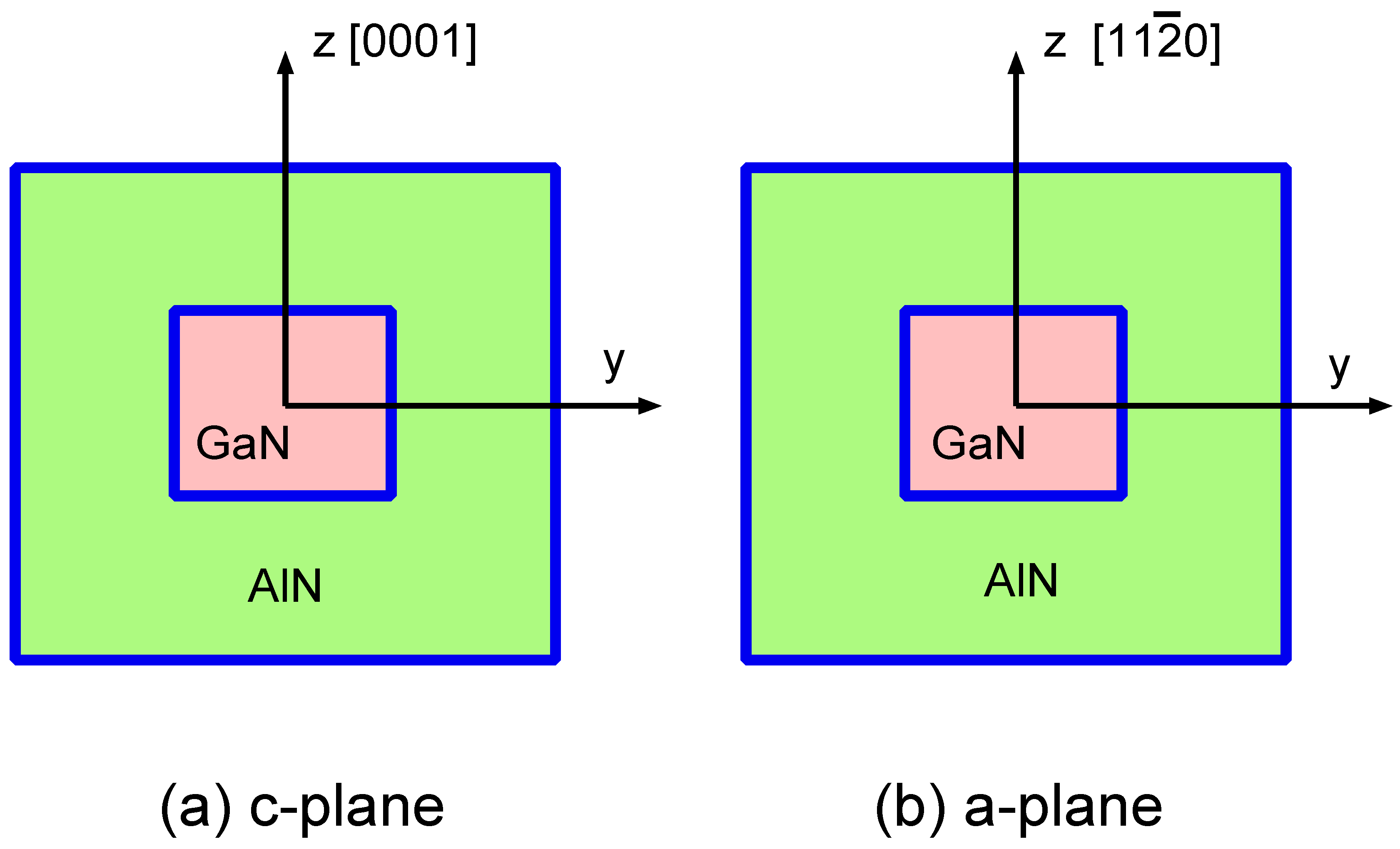
In this paper, we investigate screening potential arising from the internal field and light emission characteristics of non-polar WZ GaN/AlN QDs by using multi-band effective mass theory. The wavefunctions are obtained by solving the Schrödinger equation for electrons and the Hamiltonian for holes [14,15] adopted for the QD structure. We consider a cubic QD structure (GaN) grown on GaN of a length d, which is embedded in AlN cladding material with a size of ). In Figure 1, we plotted schematic geometry for (a) c-plane and (b) a-plane QD structures. The growth axes for c-plane and a-plane correspond to (0001)- and -orientations.
2. Theory
2.1. (0001)-Oriented Hamiltonian and Built-in Potential
The (0001)-oriented c-plane Hamiltonian for the valence-band structure can be written as [14,15]
where
Here, is the crystal-field split energy, and account for spin-orbit interactions, the ’s are the valence-band effective-mass parameters, the ’s are the deformation potentials for wurtzite crystals, is the wave vector, and is the strain tensor. Here, and , which are due to mismatches between the lattice constants of the well ( and ) and the substrate ( and ). The bases for the Hamiltonian are defined as
The strain tensors and built-in potential are obtained by [16]
where are vectors of the stress, C is the elastic stiffness tensor, e is the piezoelectric constant tensor, and D is the electric flux, which are related to the strain and electric field E vectors. Here, , , and are the piezoelectric polarization, relative dielectric constants, and spontaneous polarization, respectively.
2.2. (110)-Oriented-Oriented Hamiltonian
The Hamiltonian for an arbitrary crystal orientation can be obtained using a rotation matrix
Rotations of the Euler angles and transform the physical quantities from coordinates to coordinates. The z-axis corresponds to the c-axis [0001]. The relation between the coordinate systems for vectors and tensors is expressed as [17,18,19]
where summation over repeated indices is indicated. The a-plane Hamiltonian with a set of faces can be obtained by substituting and into Equation (1). The misfit strain, , of the QD is taken with respect to the surrounding matrix and is assumed to be equal to , where is the misfit strain in the plane and is the misfit strain along the z plane [20].
2.3. Self-Consistent Calculation
The total potential profiles for the electrons and holes are [21]
where and are the square potential for the conduction band and valence band, respectively, V is the static electric potential induced by the piezoelectric and spontaneous polarizations, and is the screening potential induced by the charged carriers, which satisfies Poisson’s equation
where is the dielectric constant. The density of state for a quantum dot is given by , where V is the volume of the QD. Then, the quasi-Fermi levels for a given carrier density are calculated from the charge neutrality using the following relations [16]:
where and are the relevant quasi-Fermi levels. Here, we assumed that carriers are injected into the QD and the contribution from continuum states is negligible in Equation (12). The electron and hole concentrations, and , in Equation (11) are related to the wavefunctions of the n-th conduction subband and the m-th valence subband by [16]
and
where refers to the bases for the Hamiltonian, and (, and 6) are envelope functions in the conduction and valence bands, respectively.
2.4. Optical Matrix Element and Spontaneous Emission Coefficient
The optical momentum matrix elements for the QD are given by [15]
where and are the wave functions for the conduction and the valence bands, respectively. The indices and denote the electron states in the conduction band and the subband states in the valence band, respectively. The polarization-dependent interband momentum-matrix elements can be written as
TE -polarization ():
TM -polarization ( ):
Furthermore,
The spontaneous emission coefficient for the quantum dot is [1]
where is the free-electron mass, is the angular frequency, is the vacuum permeability, and is the intraband relaxation time, which is assumed to be s.
3. Results
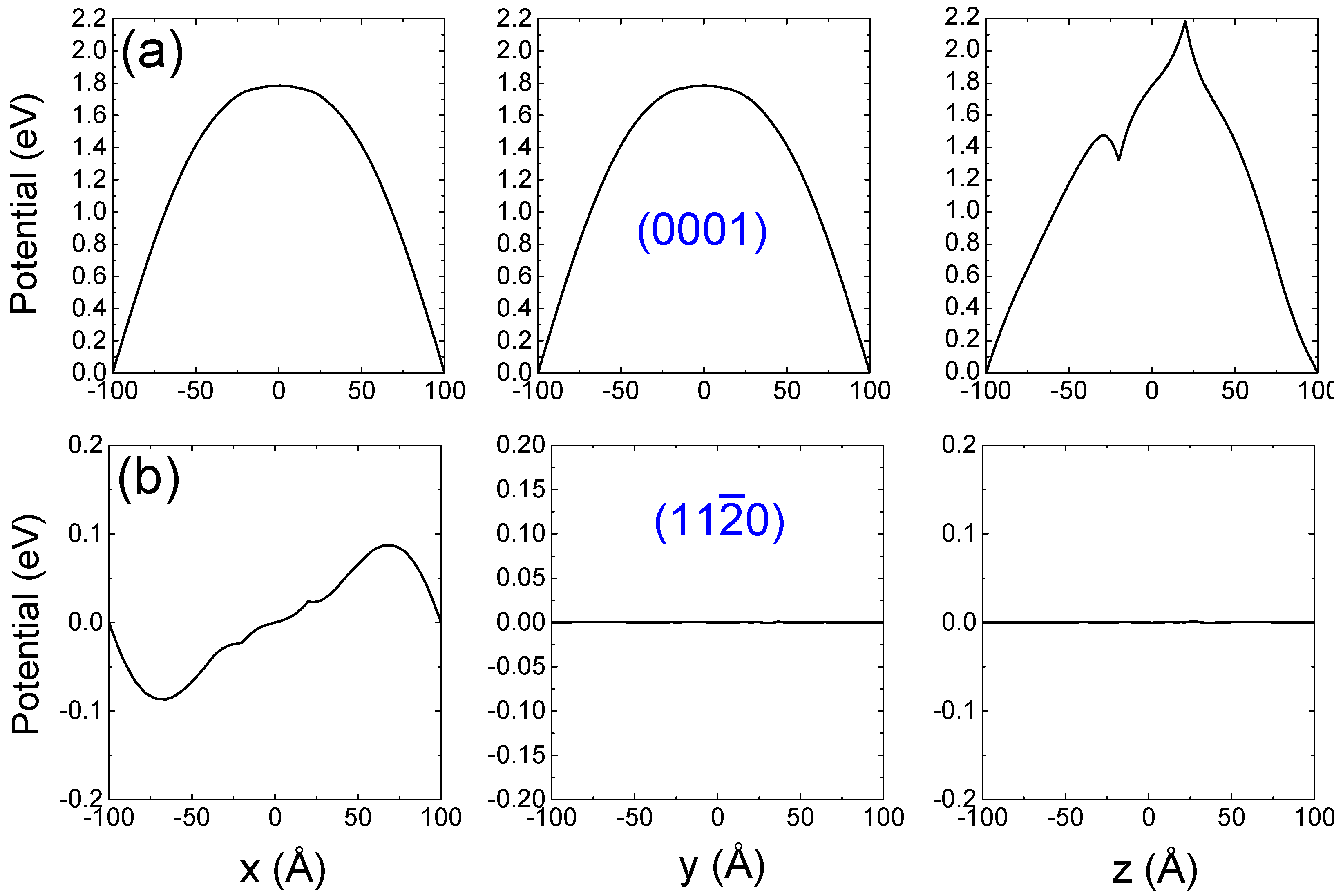
Figure 2 shows the calculated potential along x-, y-, and z-axes for (a) (0001)- and (b) (110)-oriented GaN/AlN QD structures grown on GaN substrate. The length d of cubic QD is set to be 40 . The (0001)-oriented GaN/AlN QD structure shows that there exists a large potential along x-, y-, and z-axes. The potentials along x- and y-axes are mainly due to the strain-induced piezoelectric polarization. In the case of the potential along z-axis, its magnitude is observed to be slightly larger than that along x- or y-axis because there exists a spontaneous polarization along z-axis. On the other hand, in the case of the (110)-oriented GaN/AlN QD structure, the dominant potential is observed for the case along x-axis only because the spontaneous polarization is toward the polar [0001] direction and the strain-induced piezoelectric polarization is small. As a result, we expect that the internal field effect can be reduced for the non-polar GaN/AlN QD structure.
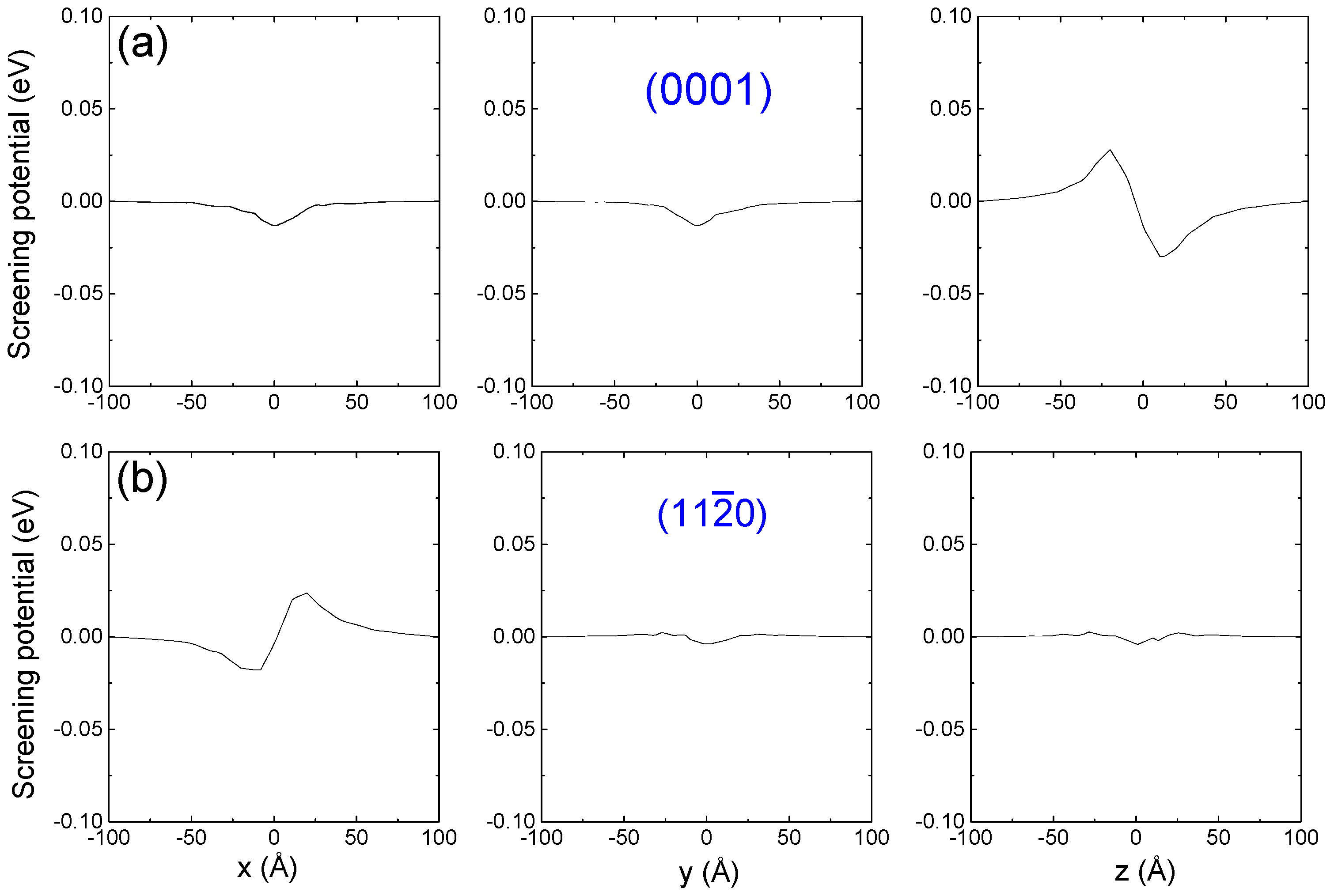
Figure 3 shows the screening potential along x-, y-, and z-axes for (a) (0001)- and (b) (110)-oriented a-plane GaN/AlN QD structures grown on GaN substrate. The (0001)-oriented GaN/AlN QD structure shows that the screening potential along z-axis is larger than that along x- or y-axis because there exists larger internal field along z-axis due to the spontaneous polarization. In the case of the (110)-oriented GaN/AlN QD structure, however, dominant screening potential is observed along x-axis while the screening potential along y- or z-axis is relatively small. The magnitude of the screening potential may be related to the magnitude of the potential due to the PZ and SP polarizations. Furthermore, the increase in the screening potential will affect the optical matrix elements.
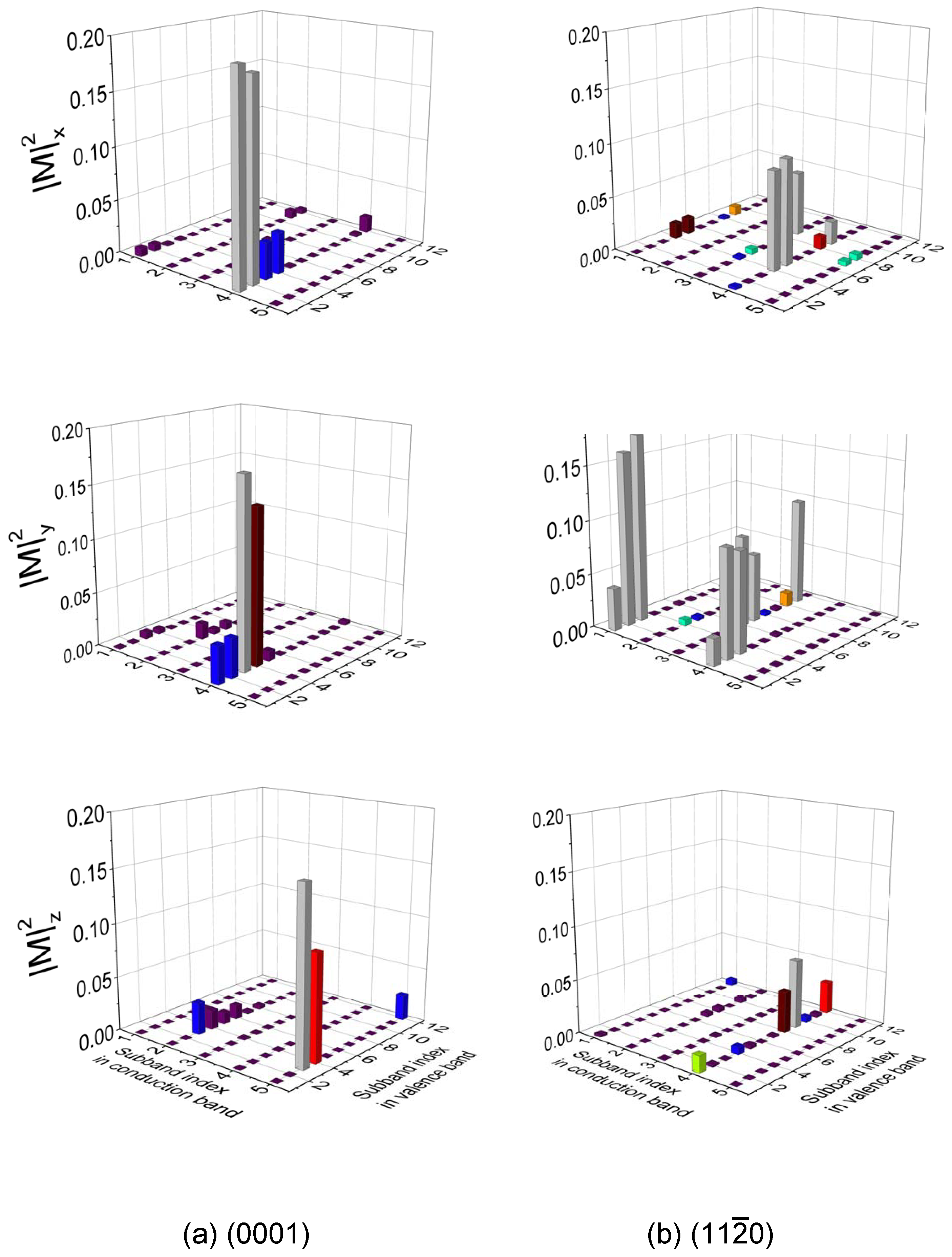
Figure 4 shows the normalized optical matrix element for x-, y-, and z-polarization for (a) (0001)- and (b) (110)-oriented a-plane GaN/AlN QD structures grown on GaN substrate. The x or y coordinate indicates the subband index in the conduction and valence bands. (i,j) means that the matrix element corresponds to the transition between i-th subband in the conduction band and j-th subband in the valence band. The quasi-Fermi levels in the conduction and valence bands are located below the first subband for both (0001)- and (110)-oriented QD structures. That is, energy spacings between the quasi-Fermi energy and the first subband are −0.020 and −0.042 eV for the conduction and valence bands in the (0001)-oriented QD structure, respectively. Similar results are obtained for the (110)-oriented QD structure. Thus, in the case of the conduction band, we plotted only two subbands because the energy spacing between subbands is large (∼0.24 eV). On the other hand, in the case of the valence band, we plotted twelve subbands because the energy spacings between subbands are very small (∼0.005).
In the case of the x-polarization, the (0001)-oriented GaN/AlN QD structure shows that dominant matrix elements are related to transition between the first subband in conduction and the first two valence bands. On the other hand, the (110)-oriented QD structure shows that the matrix elements related to transition between the first subband in conduction and the 4- and 5-th valence bands are dominant and larger than those of the (0001)-oriented GaN/AlN QD structure. However, the (0001)-oriented GaN/AlN QD structure shows that x-polarized light intensity is larger than that of the (110)-oriented QD structure. This means that matrix elements related to the transition between lower subbands are important because carrier population in higher subbands is low. On the other hand, the (110)-oriented GaN/AlN QD structure shows much larger y-polarized matrix elements than the (0001)-oriented GaN/AlN QD structure, which is related to the transition between lower subbands. Thus, the y-polarized light intensity for the GaN/AlN QD structure is about four times larger than that for the (0001)-oriented GaN/AlN QD structure. Similar tendency is observed for the case of the z-polarization.
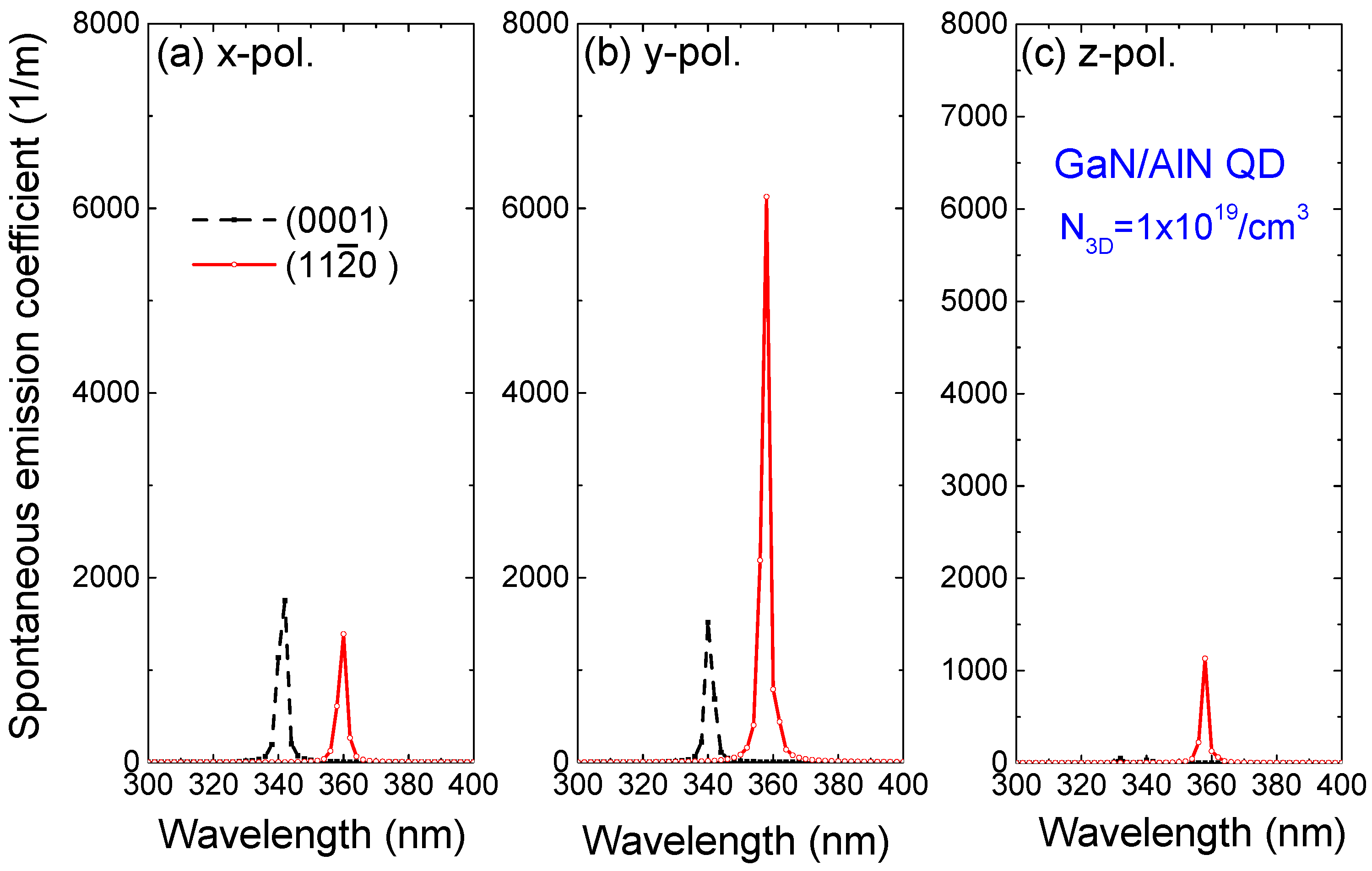
Figure 5 shows the spontaneous emission spectra for x-, y-, and z-polarizations for (0001)- and (110)-oriented a-plane GaN/AlN QD structures grown on GaN substrate. Spontaneous emission coefficients are calculated at the carrier density of N = 1 . The (0001)-oriented GaN/AlN QD structure shows that x- or y-polarized light intensity is much larger than z-polarized light intensity. This is because the optical matrix element for x- or y-polarization between ground state subbands is relatively larger than that for the z-polarization. On the other hand, the (110)-oriented GaN/AlN QD structure shows that the light intensity for y-polarization is dominant. Furthermore, we observe that the y- or z-polarized light intensity for the (110)-oriented GaN/AlN QD structure is four times larger than that for the (0001)-oriented GaN/AlN QD structure. Thus, we expect that non-polar GaN/AlN QD structure can be used for optoelectonic device with high light intensity, as observed for QW structures.
4. Conclusions
We investigated screening potential and light emission characteristics of non-polar WZ GaN/AlN QDs by using an effective mass theory. The (0001)-oriented GaN/AlN QD structure shows that the screening potential along z-axis is larger than that along x- or y-axis because there exists larger internal field along z-axis. In the case of the (110)-oriented GaN/AlN QD structure, however, the screening potential along x-axis is large while the screening potential along y- or z-axis is very small. The light intensity for the a-plane GaN/AlN QD structure is shown to be about four times larger than that for the (0001)-oriented GaN/AlN QD structure because the internal field of the former is reduced, compared to that of the latter. We expect that non-polar GaN/AlN QD structure can be used for optoelectonic device with high light intensity, as observed for QW structures.
Author Contributions
S.-H.P. contributed software and data calculations and D.A. contributed writing and editing. All authors have read and agreed to the published version of the manuscript.
Funding
S.-H.P. was supported by Basic Science Research Program through the National Research Foundation of Korea(NRF) funded by the Ministry of Education, Science and Technology(2018R1D1A1B07042028). D.A. is supported by the 2017 Research Grant from the University of Seoul.
Conflicts of Interest
There is no conflict of interest.
References
- Bimberg, D.; Grundmann, M.; Ledentsov, N.N. Quantum Dot Heterostructure; Wiley: New York, NY, USA, 1999. [Google Scholar]
- Marquardt, O.; Hickel, T.; Neugebauer, J. Polarization-induced charge carrier separation in polar and nonpolar grown GaN quantum dots. J. Appl. Phys. 2009, 106, 083707. [Google Scholar] [CrossRef]
- Schulz, S.; Berube, A.; O’Reilly, E.P. Polarization fields in nitride-based quantum dots grown on nonpolar substrates. Phys. Rev. B 2009, 79, 081401. [Google Scholar] [CrossRef]
- Schulz, S.; O’Reilly, E.P. Built-in fields in non-polar InxGa1-xN quantum dots. Phys. Status Solidi C 2010, 7. [Google Scholar] [CrossRef]
- Caro, M.A.; Schulz, S.; Healy, S.; O’Reilly, E.P. Built-in field control in alloyed c-plane III-N quantum dots and wells. J. Appl. Phys. 2011, 109, 084110. [Google Scholar] [CrossRef]
- Young, T.D.; Jurczak, G.; Lotsari, A.; Dimitrakopulos, G.P.; Komninou, P.; Dłużewski, P. A study of the piezoelectric properties of semipolar 1122 GaN/AlN quantum dots. Phys. Status Solidi B 2015, 252, 2296–2303. [Google Scholar] [CrossRef]
- Budagosky, J.A.; Garro, N.; Cros, A.; García-Cristóbal, A.; Fount, S.; Daudin, B. Optical properties of wurtzite GaN/AlN quantum dots grown on non-polar planes: The effect of stacking faults in the reduction of the internal electric field. Mater. Sci. Semicond. Process. 2016, 49, 76–80. [Google Scholar] [CrossRef] [Green Version]
- Bernardini, F.; Fiorentini, V.; Vanderbilt, D. Spontaneous polarization and piezoelectric constants of III-V nitrides. Phys. Rev. B 1997, 56, 10024. [Google Scholar] [CrossRef] [Green Version]
- Martin, G.; Botchkarev, A.; Rockett, A.; Morkoc, H. Valence-band discontinuities of wurtzite GaN, AlN, and InN heterojunctions measured by x-ray photoemission spectroscopy. Appl. Phys. Lett. 1996, 68, 2541. [Google Scholar] [CrossRef]
- Park, S.-H. Crystal orientation effects on electronic properties of Wurtzite GaN/AlGaN quantum wells with spontaneous and piezoelectric polarization. Jpn. J. Appl. Phys. 2000, 39, 3478. [Google Scholar] [CrossRef]
- Waltereit, P.; Brandt, O.; Trampert, A.; Grahn, H.T.; Menniger, J.; Ramsteiner, M.; Reiche, M.; Ploog, K.H. Nitride semiconductors free of electrostatic fields for efficient white light-emitting diodes. Nature 2000, 406, 865. [Google Scholar] [CrossRef] [PubMed]
- Su, G.L.; Frost, T.; Bhattacharya, P.; Dallesasse, J.M.; Chuang, S.L. Detailed model for the In0.18Ga0.82N/GaN self-assembled quantum dot active material for λ = 420 nm emission. Opt. Express 2014, 22, 22716. [Google Scholar] [CrossRef] [PubMed]
- Park, S.-H.; Ahn, D. Screening effects on the optical properties of II-VI wurtzite ZnO/MgO quantum dots. Phys. Rev. B 2018, 97, 075301. [Google Scholar] [CrossRef]
- Chuang, S.L.; Chang, C.S. k·p method for strained wurtzite semiconductors. Phys. Rev. B 1996, 54, 2491. [Google Scholar] [CrossRef] [PubMed]
- Park, S.-H.; Chuang, S.L. Crystal-orientation effects on the piezoelectric field and electronic properties of strained wurtzite semiconductors. Phys. Rev. B 1999, 59, 4725. [Google Scholar] [CrossRef]
- Boxberg, F.; Tulkki, J. Theory of the electronic structure and carrier dynamics of strain-induced (Ga, In)As quantum dots. Rep. Prog. Phys. 2007, 70, 1425. [Google Scholar] [CrossRef] [Green Version]
- Hinckley, J.M.; Singh, J. Influence of substrate composition and crystallographic orientation on the band structure of pseudomorphic Si-Ge alloy films. Phys. Rev. B 1990, 42, 3546. [Google Scholar] [CrossRef] [PubMed]
- Nye, J.F. Physical Properties of Crystals; Clarendon: Oxford, UK, 1989. [Google Scholar]
- Hong, K.B.; Kuo, M.K. Effect of piezoelectric constants in electronic structures of InGaN quantum dots. Semicond. Sci. Technol. 2013, 28, 105006. [Google Scholar] [CrossRef]
- Williams, D.P.; Andreev, A.D.; O’Reilly, E.P.; Faux, D.A. Derivation of built-in polarization potentials in nitride-based semiconductor quantum dots. Phys. Rev. B 2005, 72, 235318. [Google Scholar] [CrossRef] [Green Version]
- Park, S.-H.; Chuang, S.L. Piezoelectric effects on electrical and optical properties of wurtzite GaN/AlGaN quantum well lasers. Appl. Phys. Lett. 1998, 72, 3103. [Google Scholar] [CrossRef]
Figure 1.
Schematic geometry for (a) c-plane and (b) a-plane QD structures.

Figure 2.
Calculated potential along x-, y-, and z-axes for (a) (0001)- and (b) (110)-oriented GaN/AlN QD structures grown on GaN substrate. The length d of cubic QD is set to be 40 .
Figure 2.
Calculated potential along x-, y-, and z-axes for (a) (0001)- and (b) (110)-oriented GaN/AlN QD structures grown on GaN substrate. The length d of cubic QD is set to be 40 .

Figure 3.
Screening potential along x-, y-, and z-axes for (a) (0001)- and (b) (110)-oriented a-plane GaN/AlN QD structures grown on GaN substrate.
Figure 3.
Screening potential along x-, y-, and z-axes for (a) (0001)- and (b) (110)-oriented a-plane GaN/AlN QD structures grown on GaN substrate.

Figure 4.
Normalized optical matrix element for x-, y-, and z-polarization for (a) (0001)- and (b) (110)-oriented a-plane GaN/AlN QD structures grown on GaN substrate.
Figure 4.
Normalized optical matrix element for x-, y-, and z-polarization for (a) (0001)- and (b) (110)-oriented a-plane GaN/AlN QD structures grown on GaN substrate.

Figure 5.
Spontaneous emission spectra for x-, y-, and z-polarizations for (0001)- and (110)-oriented a-plane GaN/AlN QD structures grown on GaN substrate.
Figure 5.
Spontaneous emission spectra for x-, y-, and z-polarizations for (0001)- and (110)-oriented a-plane GaN/AlN QD structures grown on GaN substrate.

© 2020 by the authors. Licensee MDPI, Basel, Switzerland. This article is an open access article distributed under the terms and conditions of the Creative Commons Attribution (CC BY) license (http://creativecommons.org/licenses/by/4.0/).
Share and Cite
MDPI and ACS Style
Park, S.-H.; Ahn, D. Non-Polar Wurtzite (1120) GaN/AlN Quantum Dots for Highly Efficient Opto-Electronic Devices. Electronics 2020, 9, 1256. https://doi.org/10.3390/electronics9081256
AMA Style
Park S-H, Ahn D. Non-Polar Wurtzite (1120) GaN/AlN Quantum Dots for Highly Efficient Opto-Electronic Devices. Electronics. 2020; 9(8):1256. https://doi.org/10.3390/electronics9081256
Chicago/Turabian StylePark, Seoung-Hwan, and Doyeol Ahn. 2020. "Non-Polar Wurtzite (1120) GaN/AlN Quantum Dots for Highly Efficient Opto-Electronic Devices" Electronics 9, no. 8: 1256. https://doi.org/10.3390/electronics9081256
Note that from the first issue of 2016, this journal uses article numbers instead of page numbers. See further details here.