Erect Au Nanocones Drawn from Au Nano-Films by Nano-Size Au-Si Eutectic Clamping with High Adhesion to Substrates
by
 ,
,
Xinxiang Yu
1,2 ,
,
Zhiguo Zhao
3,
Dandan Shi
3,
Xiaoyan Dong
1,
Xianli Shi
1,
Junfeng Zhao
1,2 and
Han Dai
1,2,* 1
Laboratory of Advanced Light Alloy Materials and Devices, Postdoctoral Workstation of Nanshan Group Co., Ltd. Yantai Nanshan University, Longkou 265713, China
2
School of Materials & Engineering, Shandong University, Jinan 250100, China
3
Hang Xin Material Technology Co. Ltd., Longkou 264006, China
*
Author to whom correspondence should be addressed.
Metals 2020, 10(8), 1042; https://doi.org/10.3390/met10081042
Submission received: 15 July 2020
/
Revised: 27 July 2020
/
Accepted: 29 July 2020
/
Published: 3 August 2020
Abstract
:Erect Au nanocones with high adhesion to substrates are obtained by simply drawing from Au nano-films through Au-Si eutectic welding. Nanocones with diameters ranging from about 5 to 150 nm and length ranging from about 60 to 600 nm can be observed on both Au and Si substrate surfaces. Nano-scale Au-Si eutectics formed at the rough Au–silicon film interface under annealing at 450 °C and the subsequent cooling process facilitate the formation of nano-bonding points and draw Au nanocones from Au nano-film by mechanical separation. Erect Au nanocones adhered to Au or Si substrates shows higher light enhancement than itself, observed by FDTD simulation. This method provides new strategy for the fabrication of SERS detectors, solar cells et al. with high stability.
1. Introduction
Au nanocones with fairly distinguished light enhancement resulting from their sharp tip have attracted a lot of attention in Surface-Enhanced Raman Scattering (SERS) detectors, solar cells for light management [1,2]. Many approaches, including electron beam lithography, nano-transfer printing, nano-imprint fabrication, ultrasound assisted interfacial synthesis and evaporation coating by Anodic Aluminum Oxide (AAO) templates, have been adopted to fabricate erect Au nanocones [3,4,5,6,7]. In addition to the sophisticated processes or huge costs of these methods, the low adhesion of Au nanocones with substrates seems unavoidable due to the lack of welding through annealing processes in most methods. The reason why annealing cannot be used to improve the adhesion of erect Au nanocones with substrates is because of the low temperature ripening of Au nanocones due to the size effect [8]. Even under relatively low temperature annealing, the morphologies of Au nanocones could be easily changed. Apparently, such low adhesion can significantly limit the stability or even service life of the devices.
It is well known that Au is the most malleable metal on earth. Traditionally, fine Au wires (diameters about dozens of microns) can be easily obtained by common cold drawing technology by die [9]. To some extent, the hole diameter of the die determines the size limit that the wires can reach. At the same time, it is necessary to ensure that the wire traction end can achieve effective clamping [10]. In this situation, Au wire generally has a very high adhesion fixed with either the clamping end or the gold base, which provides us the inspiration for obtaining Au nanowires with high adhesion on substrates by nano-drawing. However, this poses an obvious challenge of obtaining nano-size clamping ends on a large scale. Fortunately, the morphologies of wet etching holes (often with diameters ranging from several nanometres to microns) of most common semiconductors Si could be adopted and used as clamping ends [11]. Additionally, Au that has entered into these holes can be held tightly by the formation of mountains of strong Au-Si eutectic [12] between the interfaces after simply low temperature annealing. With mechanical separation of Au from Si substrate by nano-size drawing, erect Au nanocones with high adhesion on both Si and Au substrates could be obtained.
2. Materials and Methods
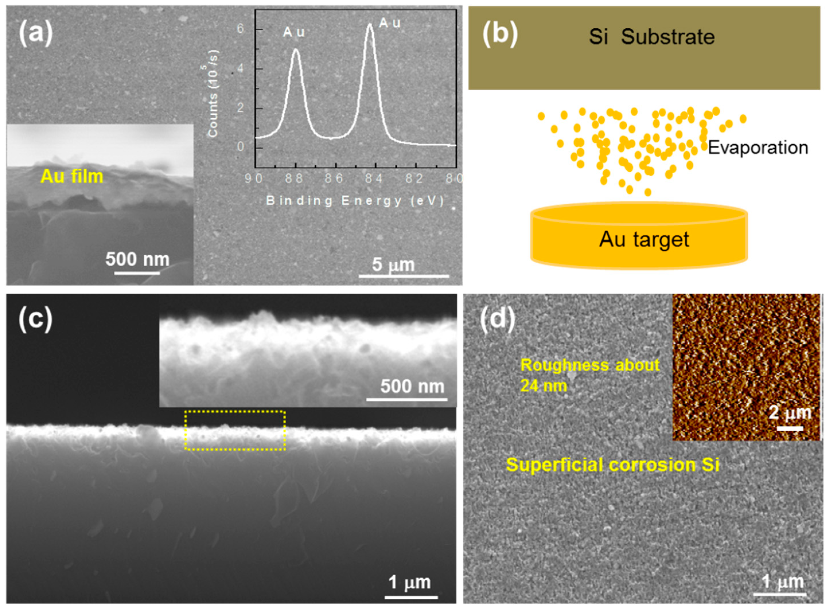
Porous Si substrate was fabricated by Au nano-film assisted wet etching of n-type silicon wafer with (111) orientation. Firstly, the oxide layer and impurities on Si substrate were cleaned by the Radio Corporation of America method [13]. Au nano-films with a thickness of about 100 nm were fabricated on Si surface through e-beam evaporation, as shown in Figure 1a,b. Then, samples were directly immersed into etchant (with volume ratio, HF:H2O2:H2O = 1:5:10) for 2 min at room temperature. Due to the lax structure of Au nano-films, the etchant easily went down to Si substrate and etched Si surface assisted by Au nano-films. After removing Au nano-film by aqua regia, the top views of Si substrate with porous structures are presented in Figure 1c,d. Through atomic force microscopy test, the roughness of Si surface is about 24 nm after the wet etching. The surface area of porous Si is about 160 m2/g, which was measured using a surface area analyzer (Jingxin, JB-2020, Chongqing, China,) based on the nitrogen adsorption method. Similarly to metal nanoparticle assisted etching [14], partial Au nano-film as catalyst was immersed into these nano-size porous structures during the etching process. Apparently, the etching treatment on Au/Si will significantly extend their interfacial contact area. Then, samples were annealed under 450 °C and erect Au nanocones were drawn out by the cold drawing process, which were presented detail in the results and discussion part below.
Simulations based on finite difference time domain method (FDTD) of the near field light enhancement of Au nanocones were performed. In our model, the electromagnetic pulse fixed at 785 nm was launched into a box containing the target Au nanocones with Si and Au substrate to simulate their near field light enhancement. The overlap region of gold tip was divided into 10 nm meshes. The refractive index of the surrounding medium was taken to be 1.0. The Au nanocones were modeled 100 nm length with 40 nm diameter according to the measurements. The morphology of Au nanocone, porous Si and Au nano-films were characterized with a field emission scanning electron microscope (SEM, Hitachi UHR FE-SEM SU8010, Tokyo, Japan). The element of Au nano-films was measured using an X-ray photoelectron spectrometer (XPS, Escalab 250Xi, Waltham, MA, USA).
3. Results and Discussion
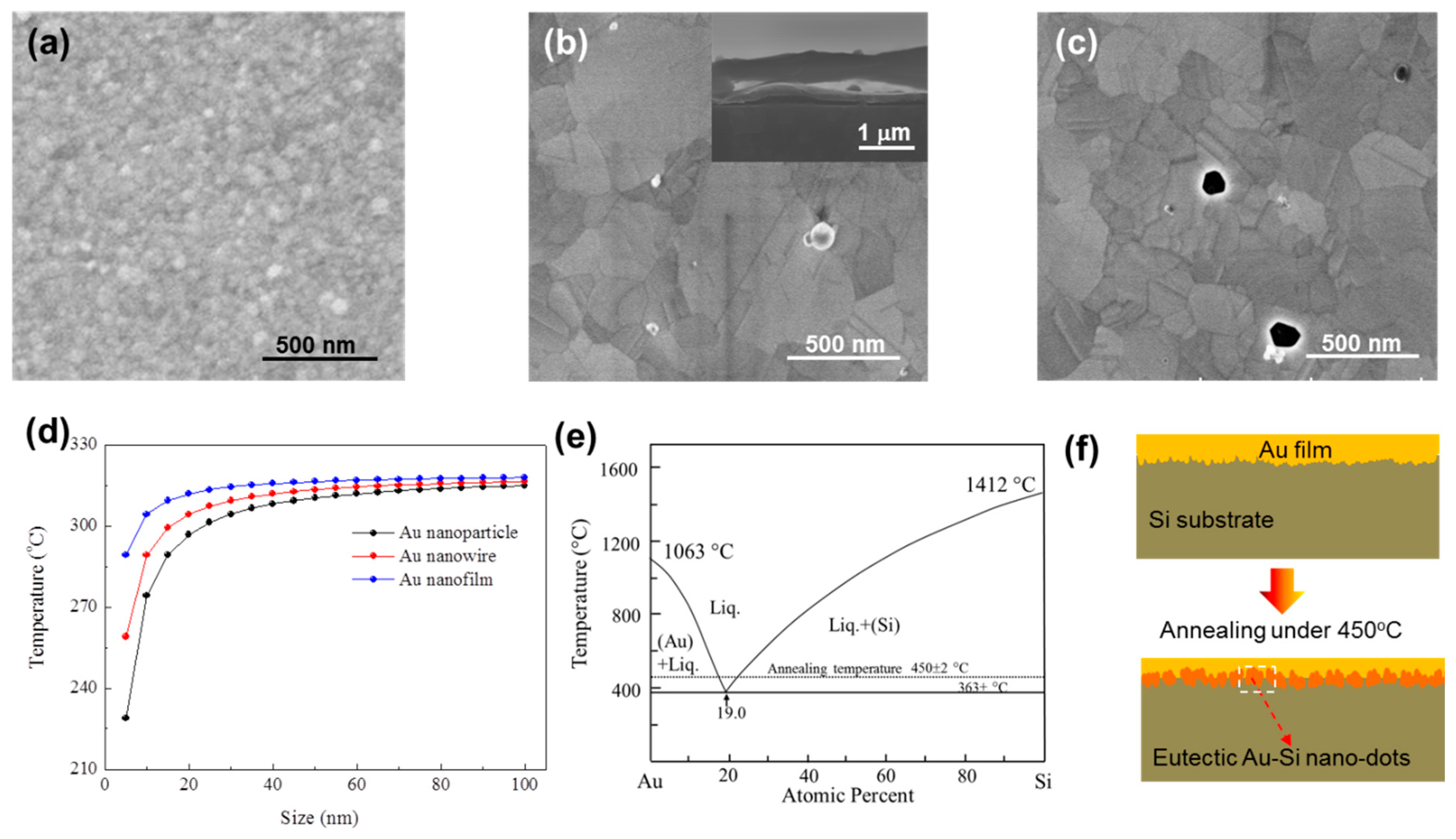
Although the immersed Au nano-film in nano-size porous Si (160 m2/g) obtained by wet etching make the contact area even 104 larger than the smooth Si surface (0.0034 m2/g), the lax structure of Au nano-film and weak adhesion at the Au/Si interface make it difficult to draw Au nanocone out of Au nano-film. To resolve these problems, samples were annealed under 450 °C to obtain compacted Au nano-film and reliable binding points at the Au/Si interface. As shown in Figure 2a–c, the lax structure of Au nano-film composed by mountains of nanoparticles with diameters of several nanometers can be easily melted and ripened into compacted polycrystalline, thereby significantly enhancing the compactability of Au nano-film. The size of Au nanoparticles in the lax structure of Au nano-film increases significantly during this annealing process. The ripening temperature (partial melting) of Au nano-film greatly increases to the bulk ripening point due to their micro-structure changes, as shown in Figure 2d. This significant increase in the ripening temperature of Au polycrystalline could inhibit its further growth [15]. Owing to this, submicron crystals (average gain size is about 502 ± 15 nm, statistical scope is about 121 μm2) in Au polycrystalline nano-films can be observed in Figure 2b,c. The annealing twins and shrinkage cavities formed in Au nano-film could be attributed to the effect of non-uniform high surface tensions, which is similar with the intrinsic stress induced by high strain rolling in metals with low stacking fault energy [16]. During the annealing, the contents of Si atoms solid dissolved into Au nano-film close to the Au/Si interface dominated the number and size of Au-Si eutectics at Au/Si interfaces [17]. The ripening process of Au nano-film provides the opportunity to weld Au nano-film with Si substrate through the formation of Au-Si eutectic. Due to the ripening of Au nano-film and the super large interface between Au nano-film/porous Si, the diffusion capacity of Si into the holes of porous silicon which is filled with Au is significantly enhanced. Owing to the much higher percentage of Si atoms dissolved in Au nano-film, mountains of nano-size Au-Si eutectic welding points can be formed at Au/Si interfaces in the holes of porous silicon according to the Au-Si binary phase diagram in Figure 2e [18]. A schematic image of the Au-Si eutectics formed in Au nano-film/porous Si interface has been provided in Figure 2f, which can be used to understand this welding process. Apparently, these Au-Si eutectic welding points in Au nano-film/porous Si interface provide enough nano-size clamping ends for drawing erect Au nanocones from Au nano-films.
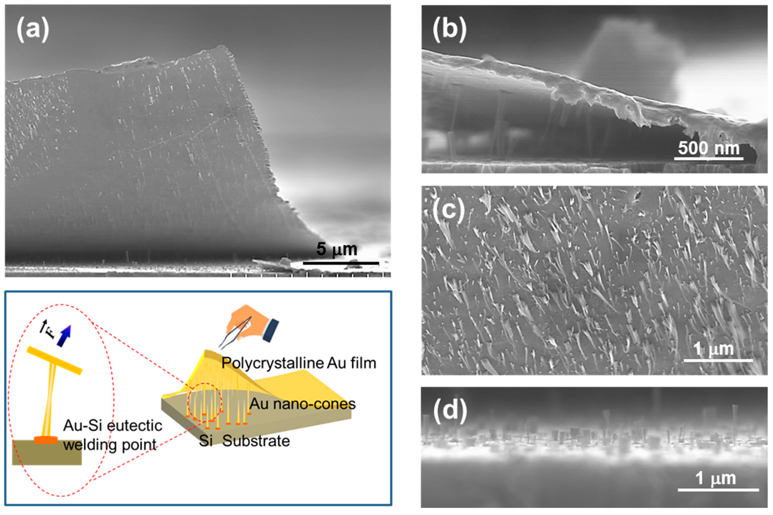
After the welding of Au nano-film/porous Si interface, erect Au nanocones can be drawn out by the cold drawing process. As shown in Figure 3a, mountains of Au nanocones can be observed on Au nano-film/porous Si interface. A schematic image is presented to show the cold drawing process of erect Au nanocones from Au nano-film, in this process, hard Au-Si eutectics formed at the Au nano-film/porous Si interface act as nano-size clamping ends. In the beginning, Au nanowires were drawn from Au nano-film due to its excellent malleable properties. After that, strain concentration begins to appear, causing necking to occur at the middle part of Au nanowires, which is presented in Figure 3b. Then, accumulative strain concentrates near the necking area, which causes the deformation instability and ultimate fracture of Au nanowires, as shown in Figure 3c,d. Even in the necking area, the cone-shaped fracture morphology can be observed on every Au nanowires after the final separation of Au nano-film/porous Si, due to the significant plastic deformation ability of Au nanowires. Note that, owing to the sizes of Au nanowires, Au nano-film should have enough thickness to provide enough blank materials and have sufficient tensile strength.
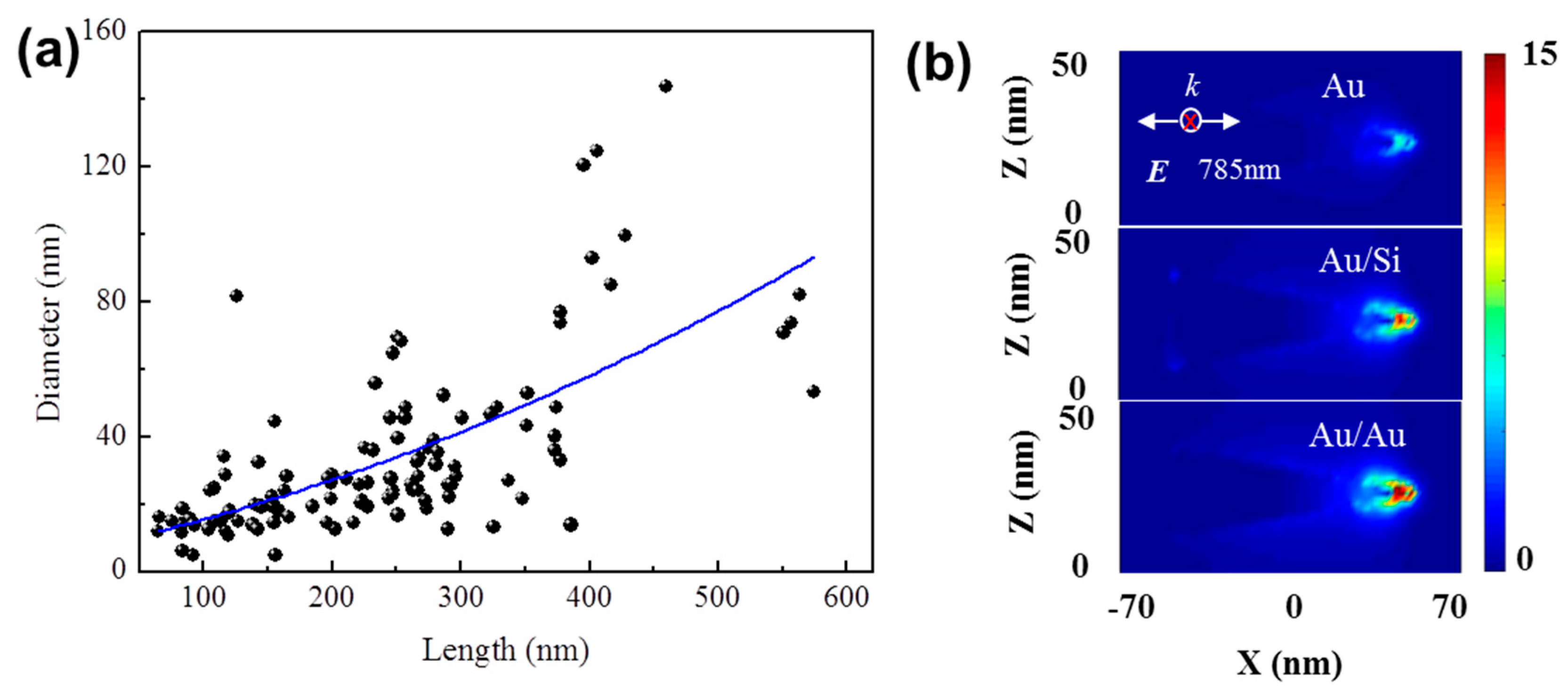
Due to the random formation of Au-Si eutectic at the Au nano-film/porous Si interface, erect Au nanocones on Au nano-films and Si substrate vary in size. Through statistics, the diameters of Au nanocones range from about 5 to 150 nm and the lengths range from about 60 to 600 nm. Near linear relation of the aspect ratio of Au nanocones can be observed in Figure 4a, which can be approximately concluded by D = 0.08L + 6.26 (standard error is about 7.95). D and L refer to the diameters and the length of Au nanocones, respectively. The deviations could be mainly attributed to the statistical error, which counts the bottom of all cones as a circle. As above, Au nanowires exhibit relatively uniform section shrinkage of the fractures surface, in other words, Au nanowires with different sizes have the same reduction in area in tensile [19]. It can be easily concluded that Au nanocones are closely attached to Au nano-film and Si substrate, which shows higher adhesion than the ultimate tensile strength of Au at least. Furthermore, Au nanocones with stable dimensions could be obtained through the controllable formation of Au-Si eutectics in specific etching areas assisted by some mask etching methods [20]. As a result, this new strategy provides a sufficient high adhesion of Au nanocones with their substrate. As reported, Au nanocones can provide significant SERS signals due to the plasmon excitation on its tip [21,22]. Through FDTD simulation (Figure 4b), Au nanocone, no matter whether it is adhered to Au nano-film or Si substrate, exhibits higher light enhancement than itself, which shows the potential use of this fabrication method in SERS detectors, solar cells et al.
4. Conclusions
In summary, we report a new way for fabricating erect Au nanocones with high adhesion to their substrate by cold drawing process. Assisted by wet etching and low temperature annealing, Au-Si eutectic welding points formed at Au nano-film/porous Si interfaces provide enough nano-size clamping ends. By simply separating Au nano-film from Si substrate mechanically, Au nanocones in various sizes can be drawn out by these clamping ends and Au nanocones can be simultaneously obtained on both Au nano-film and Si substrate. Au nanocones fabricated in this way show an adhesion with substrate at least higher than the ultimate tensile strength of Au itself. Therefore, this approach has great potential for application in durable SERS detectors, solar cells et al.
Author Contributions
Conceptualization, H.D.; methodology, X.Y.; software, J.Z.; validation, X.Y.; formal analysis, X.D.; investigation, Z.Z.; resources, D.S.; data curation, X.S.; writing—original draft preparation, H.D.; writing—review and editing, X.D.; supervision, X.S.; project administration, H.D.; funding acquisition, H.D., X.Y. and Z.Z. contribute equally to this work. All authors have read and agreed to the published version of the manuscript.
Funding
This research was funded by China Postdoctoral Science Foundation, grant number 2020M671987 and “Longkou science and technology research and development plan project, grant number 2019KJJH021.
Acknowledgments
This research study was supported by Yantai double hundred talent plan 2019 and doctoral fund of Yantai Nanshan University.
Conflicts of Interest
The authors declare no conflict of interest.
References
- Chang, W.Y.; Lin, K.H.; Wu, J.T.; Yang, S.Y.; Lee, K.L.; Wei, P.K. Novel fabrication of an Au nanocone array on polycarbonate for high performance surface-enhanced Raman scattering. J. Micromech. Microeng. 2011, 21, 035023. [Google Scholar] [CrossRef]
- Yu, M.; Long, Y.Z.; Sun, B.; Fan, Z. Recent advances in solar cells based on one-dimensional nanostructure arrays. Nanoscale 2012, 4, 2783–2796. [Google Scholar] [CrossRef] [PubMed]
- Hu, Y.S.; Jeon, J.; Seok, T.J.; Lee, S.; Hafner, J.H.; Drezek, R.A.; Choo, H. Enhanced Raman scattering from nanoparticle-decorated nanocone substrates: A practical approach to harness in-plane excitation. ACS Nano 2010, 4, 5721–5730. [Google Scholar] [CrossRef] [PubMed] [Green Version]
- Kim, T.; Kim, J.; Son, S.J.; Seo, S. Gold nanocones fabricated by nanotransfer printing and their application for field emission. Nanotechnology 2008, 19, 295302. [Google Scholar] [CrossRef] [PubMed]
- Kontio, J.M.; Husu, H.; Simonen, J.; Huttunen, M.J.; Tommila, J.; Pessa, M.; Kauranen, M. Nanoimprint fabrication of gold nanocones with ~10 nm tips for enhanced optical interactions. Opt. Lett. 2009, 34, 1979–1981. [Google Scholar] [CrossRef]
- Zhang, P.; He, J.; Ma, X.; Gong, J.; Nie, Z. Ultrasound assisted interfacial synthesis of gold nanocones. Chem. Commun. 2013, 49, 987–989. [Google Scholar] [CrossRef]
- Liu, D.; Wang, Q.; Hu, J. Fabrication and characterization of highly ordered Au nanocone array-patterned glass with enhanced SERS and hydrophobicity. Appl. Surf. Sci. 2015, 356, 364–369. [Google Scholar] [CrossRef]
- Sahu, P.; Prasad, B.L.V. Fine control of nanoparticle sizes and size distributions: Temperature and ligand effects on the digestive ripening process. Nanoscale 2013, 5, 1768–1771. [Google Scholar] [CrossRef]
- Hirakata, H.; Shimbara, K.; Kondo, T.; Minoshima, K. Size effect on tensile creep behavior of micrometer-sized single-crystal gold. Nat. Rev. Mater. 2018, 1, 221–228. [Google Scholar] [CrossRef]
- Son, S.B.; Lee, Y.K.; Kang, S.H.; Chung, H.S.; Cho, J.S.; Moon, J.T.; Oh, K.H. A numerical approach on the inclusion effects in ultrafine gold wire drawing process. Eng. Fail. Anal. 2011, 18, 1272–1278. [Google Scholar] [CrossRef]
- Ding, R.; Dai, H.; Li, M.; Huang, J.; Li, Y.; Trevor, M.; Musselman, K.P. The application of localized surface plasmons resonance in Ag nanoparticles assisted Si chemical etching. Appl. Phys. Lett. 2014, 104, 011602. [Google Scholar] [CrossRef] [Green Version]
- Wolffenbuttel, R.F. Low-temperature intermediate Au-Si wafer bonding; eutectic or silicide bond. Sens. Actuators A-Phys. 1997, 62, 680–686. [Google Scholar] [CrossRef]
- Salman, K.A.; Omar, K.; Hassan, Z. Nanocrystalline ZnO film grown on porous silicon layer by radio frequency sputtering system. Mater. Lett. 2012, 68, 51–53. [Google Scholar] [CrossRef]
- Huang, Z.; Geyer, N.; Werner, P.; De Boor, J.; Gösele, U. Metal-assisted chemical etching of silicon: A review: In memory of Prof. Ulrich Gösele. Adv. Mater. 2011, 23, 285–308. [Google Scholar] [CrossRef] [PubMed]
- Nanda, K.K.; Sahu, S.N.; Behera, S.N. Liquid-drop model for the size-dependent melting of low-dimensional systems. Phys. Rev. A 2002, 66, 013208. [Google Scholar] [CrossRef]
- Parajuli, P.; Mendoza-Cruz, R.; Velazquez-Salazar, J.J.; Yacaman, M.J.; Ponce, A. Fivefold annealing twin in nanocrystalline Au/Pd film. Mater. Lett. 2019, 244, 88–91. [Google Scholar] [CrossRef]
- Kurtuldu, G.; Löffler, J.F. Multistep crystallization and melting pathways in the free-energy landscape of a Au–Si eutectic alloy. Adv. Sci. 2020, 7, 1903544. [Google Scholar] [CrossRef]
- Okamoto, H.; Massalski, T.B. The Au−Si (Gold-Silicon) system. Bull. Alloy Phase Diagr. 1983, 190, 190–198. [Google Scholar] [CrossRef]
- Hwang, J.K. Low formability and reduction of area in twinning-induced plasticity steels despite their excellent tensile elongation. Mat. Sci. Eng. A 2020, 779, 139123. [Google Scholar] [CrossRef]
- Shingubara, S.; Okino, O.; Murakami, Y.; Sakaue, H.; Takahagi, T. Fabrication of nanohole array on Si using self-organized porous alumina mask. J. Vac. Sci. Technol. B 2001, 19, 1901–1904. [Google Scholar] [CrossRef]
- Dai, H.; Fu, P.; Li, Z.; Zhao, J.; Yu, X.; Sun, J.; Fang, H. Electricity mediated plasmonic tip engineering on single Ag nanowire for SERS. Opt. Express 2018, 26, 25031–25036. [Google Scholar] [CrossRef] [PubMed]
- Li, H.; Dai, H.; Zhang, Y.; Lee, Y.H.; Koh, C.S.L.; Phan-Quang, G.C.; Tong, W.; Zhang, Y.; Gao, H.; Ling, X.Y.; et al. Triboelectrically boosted SERS on sea-urchin-like gold clusters facilitated by a high dielectric substrate. Nano Energy 2019, 64, 103959. [Google Scholar] [CrossRef]
Figure 1.
Au nano-film deposited on Si by e-beam evaporation. (a) Top view of Au nano-film deposited on Si substrate. Profile view of Au nano-film/Si interface and the X-Ray Photoelectron Spectroscopy (XPS) analyses of Au nano-film. (b) A schematic image of the e-beam evaporation of Au onto Si surface. (c) Profile view of Si surface after etching. Inset is the magnification of porous structures, which is marked by yellow dot square. (d) Top view of the superficial corrosion of Si fabricated by wet etching process. Inset is the surface roughness of Si surface by Atomic Force Microscope (AFM).

Figure 2.
Au-Si eutectics formed at the rough Au-silicon film interface. (a) Au nano-film combined by nanoparticles on porous Si surface. (b) Au nano-film after annealing under 450 °C for 2 h. Inset is the profile view of Au nano-film/porous Si interface. (c) Contraction cavities on Au nano-film after annealing. (d) Size-depended ripening temperature of Au nanostructures. (e) Binary phase diagram of Au/Si binary alloys. (f) A schematic image of the Au-Si eutectics formed at the rough Au-silicon film interface by annealing.

Figure 3.
Cold drawing of Au nanocones from Au nano-film/porous Si interfaces. (a) Images of the cold drawing process. A schematic image of the cold drawing process. (b) Necking of Au nanowires at the Au nano-films/porous Si interfaces. (c) Profile view of Au nanocones adhered on the surface of Au nano-film. (d) Profile view of Au nanocones adhered on Si surfaces.

Figure 4.
(a) Statistical result of the aspect ratio of Au nanocones on Au nano-film. (b) Light enhancement (wavelength 785 nm) of single Au nanocone (length of 100 nm, diameter of 30 nm) and nanocone adhered to Si, Au substrates.
Figure 4.
(a) Statistical result of the aspect ratio of Au nanocones on Au nano-film. (b) Light enhancement (wavelength 785 nm) of single Au nanocone (length of 100 nm, diameter of 30 nm) and nanocone adhered to Si, Au substrates.

© 2020 by the authors. Licensee MDPI, Basel, Switzerland. This article is an open access article distributed under the terms and conditions of the Creative Commons Attribution (CC BY) license (http://creativecommons.org/licenses/by/4.0/).
Share and Cite
MDPI and ACS Style
Yu, X.; Zhao, Z.; Shi, D.; Dong, X.; Shi, X.; Zhao, J.; Dai, H. Erect Au Nanocones Drawn from Au Nano-Films by Nano-Size Au-Si Eutectic Clamping with High Adhesion to Substrates. Metals 2020, 10, 1042. https://doi.org/10.3390/met10081042
AMA Style
Yu X, Zhao Z, Shi D, Dong X, Shi X, Zhao J, Dai H. Erect Au Nanocones Drawn from Au Nano-Films by Nano-Size Au-Si Eutectic Clamping with High Adhesion to Substrates. Metals. 2020; 10(8):1042. https://doi.org/10.3390/met10081042
Chicago/Turabian StyleYu, Xinxiang, Zhiguo Zhao, Dandan Shi, Xiaoyan Dong, Xianli Shi, Junfeng Zhao, and Han Dai. 2020. "Erect Au Nanocones Drawn from Au Nano-Films by Nano-Size Au-Si Eutectic Clamping with High Adhesion to Substrates" Metals 10, no. 8: 1042. https://doi.org/10.3390/met10081042
Note that from the first issue of 2016, this journal uses article numbers instead of page numbers. See further details here.