Complex Analysis of Emission Properties of LEDs with 1D and 2D PhC Patterned by EBL
by
 ,
,
Lubos Suslik
1,* ,
,
Jaroslava Skriniarova
2,
Jaroslav Kovac
2,
Dusan Pudis
1,
Anton Kuzma
2 and
Jaroslav Kovac, Jr.
2 1
Department of Physics, Faculty of Electrical Engineering, University of Zilina, Univerzitna 1, 01026 Zilina, Slovakia
2
Institute of Electronics and Photonics, Faculty of Electrical Engineering and Information Technology, Slovak University of Technology in Bratislava, Ilkovicova 3, 81219 Bratislava, Slovakia
*
Author to whom correspondence should be addressed.
Coatings 2020, 10(8), 748; https://doi.org/10.3390/coatings10080748
Submission received: 16 July 2020
/
Revised: 24 July 2020
/
Accepted: 27 July 2020
/
Published: 30 July 2020
(This article belongs to the Special Issue Thin Films and Coatings for Energy Storage and Conversion)
Abstract
:In this paper, we present the optical and electrical properties of surface-patterned GaAs-based Multiquantum Well (MQW) light emitting diodes (LEDs) with one- and two-dimensional photonic crystal (PhC) structures. Optical properties were analyzed in the near and far field, measured by a near-field scanning optical microscope and with a goniophotometer. We demonstrated a strong effect of patterned PhC on the radiation properties and the light extraction efficiency. Enormous surface emission enhancement reaching 110% confirmed the strong effect of the patterned structure on the coupling of the guided modes into the surface emission. Additionally, the considerable effect of the PhC structure diffraction on radiation pattern was confirmed in the near and far field and is in good agreement with the simulated shape of the optical field.
1. Introduction
Intensive research to improve the radiation properties of light emitting diodes (LEDs) by surface patterning has been occurring for over a decade. Nanotechnologies brought forward solutions on how to pattern the surface on a wavelength scale with a positive effect on their efficiency and emission properties. For the most part, the LED surface patterning was aimed at efficiency improvement, because in conventional LEDs, the majority of generated light is trapped in high-refractive index confinement layers due to the total internal reflection at semiconductor–air interface. Two main treatments were used for the enhancement of extraction efficiency: (i) refractive index matching of the semiconductor–air interface and (ii) surface patterning by rough and optimized structures. Both have considerable effect on minimizing the total internal reflection of the diode surface [1,2]. The enhancement of the extraction efficiency in LEDs by surface patterning requires an optimized design leading to the photonic crystal (PhC) structures that optimize the interaction of the guided modes with the photonic band gap (PBG) of PhCs. It was achieved by different patterning techniques in original papers [3,4,5,6,7,8,9,10,11,12,13]. For maximum extraction efficiency, there must be a strong coupling between the trapped waveguide modes and PhC structure. The optimization parameters of PhC are related to the vertical structure of the LED [6,7,14], and parameters of PhCs. Firstly, the etch depth plays very important role in cross-coupling of trapped modes with the leaky Bloch modes associated with the PhC [6,8]. Additionally, the hole size, mostly known as PhC fill factor, is related to the photonic band gap of PhC and determines the extraction efficiency [9,10]. Additionally, the period of patterned PhC should be related to the photonic band gap [11]. Generally, the PhC period used in semiconductor-based LEDs is about several hundreds of nanometers.
Moreover, the choice of two-dimensional (2D) PhC geometry plays important role in determining the far-field radiation pattern of the LED [12,13]. From the point of PhC shape and geometry, the wide variety of PhC and photonic quasicrystals were investigated. Photonic quasicrystals (PQC) with a high level of symmetry produce less directional emission [9,15,16]. The recent concepts demonstrated PhC patterned in the polymer surface. Such polymer layers were successfully applied on a LED chip. Its efficiency on extraction efficiency is weak because of the low refractive index of used polymer materials and small coupling with guiding modes. However, polymer-based PhCs are interesting from the point of diffraction and radiation pattern modification and by simple application [17]. Additionally, the polymer-based technologies brought new interesting three-dimensional PhCs [18].
Such PhCs need to be defined by high-resolution lithography. The most common technique with sufficient resolution and large area patterning is interference lithography [19,20,21,22]. Another optical lithography uses the high resolution of a near field produced at the apex of the specially-prepared optical fiber probe [23]. This technique is suitable for PhC patterning in a small area, similarly known as direct-write electron-beam lithography (EBL) [24]. A very effective nanoimprint lithography for PhC fabrication was demonstrated last year [8].
In this paper, we focus on the comparison of one-dimensional (1D) and 2D PhC structures patterned by EBL in the LED surface and their effect on emission properties of AlGaAs/GaAs MQW LEDs. We bring forward a complex analysis of optical radiation properties of the PhC LED analyzed in the near and far field. The effect of the PhC structure was related to the diffraction symmetry of radiation pattern and also the light extraction efficiency.
2. Experiment
As the LED structure, we used the AlGaAs/GaAs quantum well (QW) structure with central emission wavelength at λ = 845 nm which was previously published by Hronec et al. [25]. The samples were grown by low pressure Metalorganic vapour-phase epitaxy (MOVPE) on (001) oriented n type GaAs substrates. The LED structure consists of a 1300 nm n-doped Al0.45Ga0.55As bottom confinement layer, the QW active region and 650 nm p-doped Al0.60Ga0.40As upper confinement layer. The QW active region contains three 9-nm thick GaAs QWs separated by 24-nm thick Al0.20Ga0.80As barriers. The structure was covered by a 40-nm GaAs cap layer.
The fabrication of LED chips consisted of upper ring ohmic contact metallization of p-type AuBe of thickness app. 200 nm; bottom metallization of n-type AuGeNi ohmic contact of thickness app. 200 nm; contacts annealing and MESA etching. The MESA etching was performed in etching aqueous solution of H3PO4:H2O2:H2O (3:1:50) for the isolation of the device in Figure 1.
Two different PhC LEDs based on GaAs/AlGaAs MQW structure were processed. 1D and 2D PhC structures were patterned by EBL in the surface of the LED. Each PhC has period of 700 nm. The structure First, the XR 1541 negative e-beam resist have been exposed by the ZBA 21 variable shaped e-beam pattern generator using 40 kV accelerating voltage in 50 nm resolution mode. The resist was exposed with doses ranging from 260–500 μCcm−2 and its initial thickness was 400 nm. After exposure of the resist and its development, the samples were etched by Reactive Ion Etching (RIE, Slovak Academy of Sciences, Bratislava, Slovakia) in CCl4/He based plasma. Morphological properties and quality of prepared 2D PhC structures were studied by Scanning Electron Microscopy (SEM; Jeol 7500, Slovak University of Technologhy, Bratislava, Slovakia). Optical and radiation properties were inspected in near and far field to reveal the effect of the structure on the radiation pattern using near-field scanning optical microscope (NSOM, Experimental assembled by the Department of Physics at University of Zilina, Zilina, Slovakia) and goniophotometer (Experimental assembled by the Department of Physics at University of Zilina, Zilina, Slovakia). Extraction efficiency was inspected by overall light-current L(I) measurements in Ulbrecht sphere and by detail surface emission mapping.
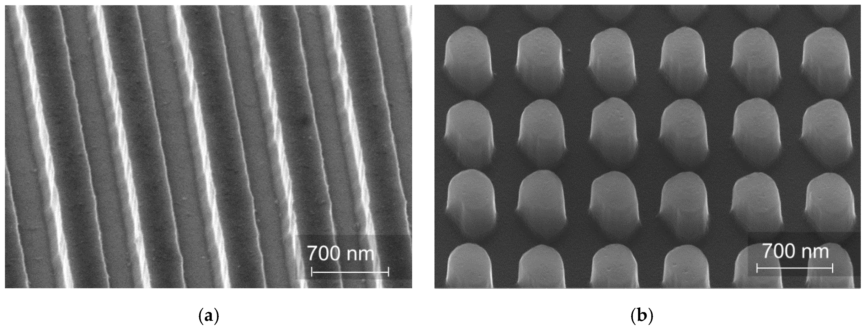
The SEM image in Figure 1 shows the top view of the emitting part of LED device with Au contact. The dark region represents the top AlGaA-emitting layer of the LED chip inside the ring contact, surrounding the contact from the outside. As can be seen from the image, the 1D PhC structure (bright grey circle) creates app. 55% of the emitting part. The detail of the 1D and 2D PhC structure is shown in Figure 2a,b, respectively. 1D PhC shows homogeneous grating with stripes of width app. 300 nm. 2D PhC consists of pillars arranged in 2D square grating. A detailed analysis of PhC structures from SEM measurements revealed more than 300 nm depth of the patterned 1D and 2D PhC structures.
3. Results and Discussion
The emitting properties of LEDs with surface-patterned 1D and 2D PhC structure were analyzed by optical measurements in the near and far field by the measurement of radiation pattern and near-field distribution. The extraction efficiency was measured in regard to L(I) characteristics.
The emitting properties of LEDs with patterned surface were investigated in the near field using the NSOM. An optical fiber probe was used, with a tapered single-mode fiber metal-coated with thin aluminum layer. Using this technique we achieved apertureless tips with diameter better than 200 nm what determines its optical resolution [23].
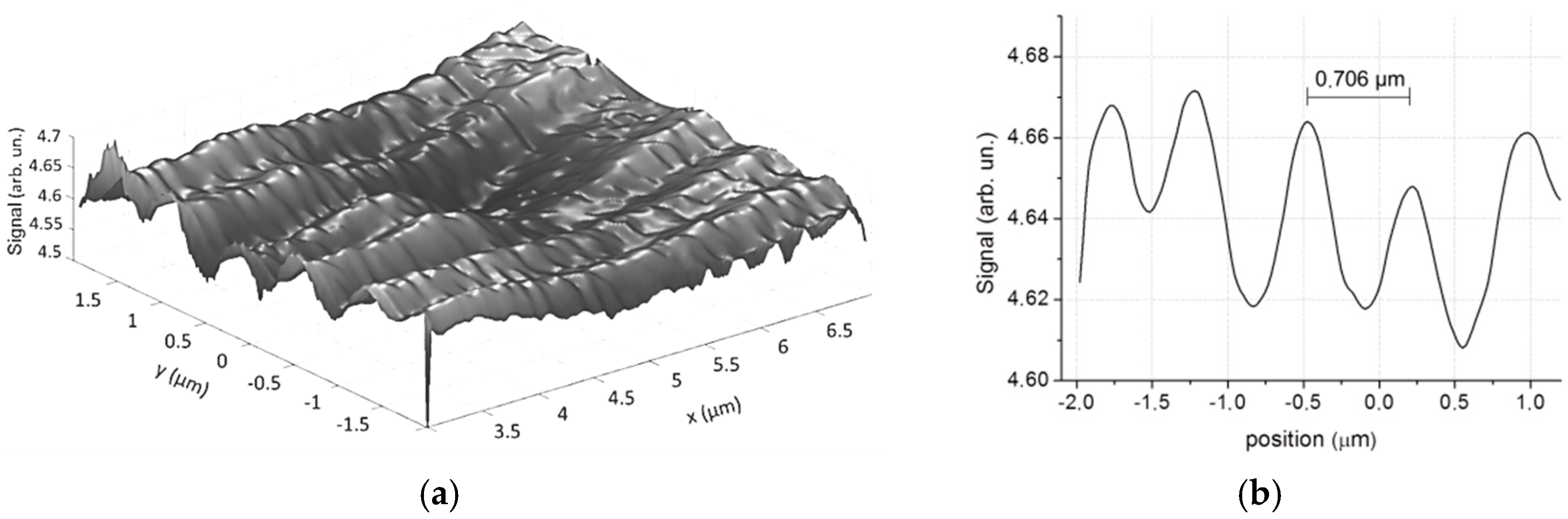
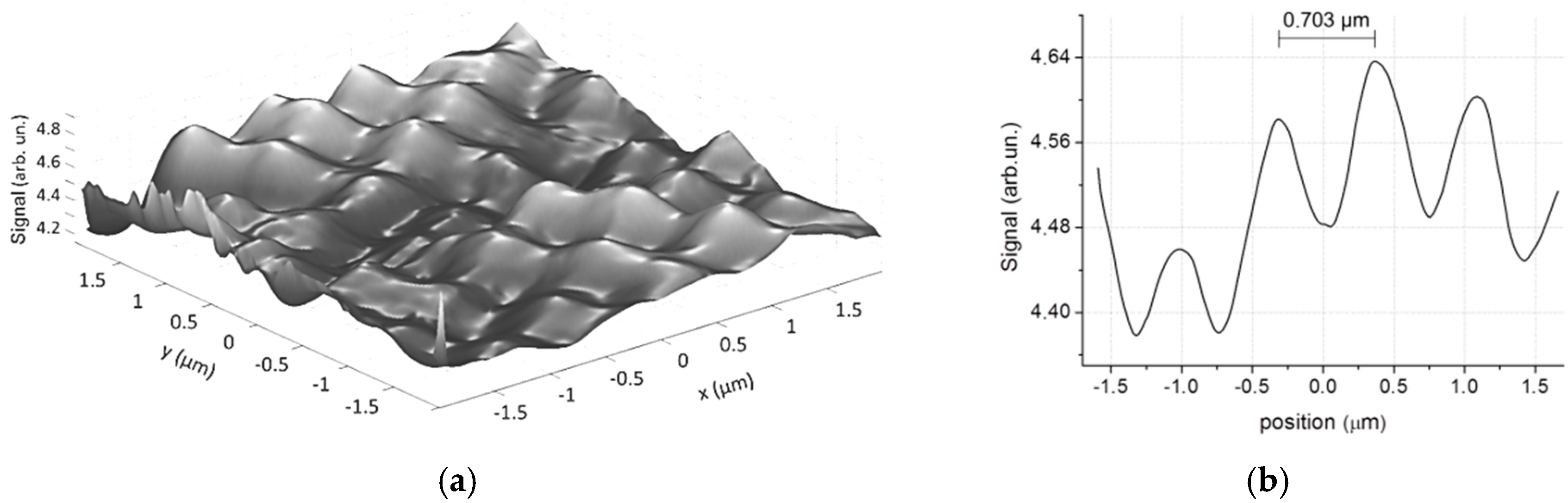
The high-resolution NSOM image revealed the local emission enhancement from the LED patterned surface with 1D PhC structure shown in Figure 3a. The line profile well documents the 700 nm period shown in Figure 3b. The amplitude of the NSOM signal modulation is relative small, however it does not directly reflect the structure effect and it is also caused by the fiber probe resolution close the line width of the 1D structure. A similar high-resolution NSOM image was obtained for the LED-patterned surface with 2D PhC structure shown in Figure 4a. Additionally, the NSOM of the 2D PhC structure shows enhancement from etched regions and documents the square symmetry of patterned structure. Line profile shows the 700 nm period illustrated at Figure 4b. The measured near field revealed enhancement from etched regions and well reflects the structure symmetry for 1D and 2D structure as was documented from SEM analysis.
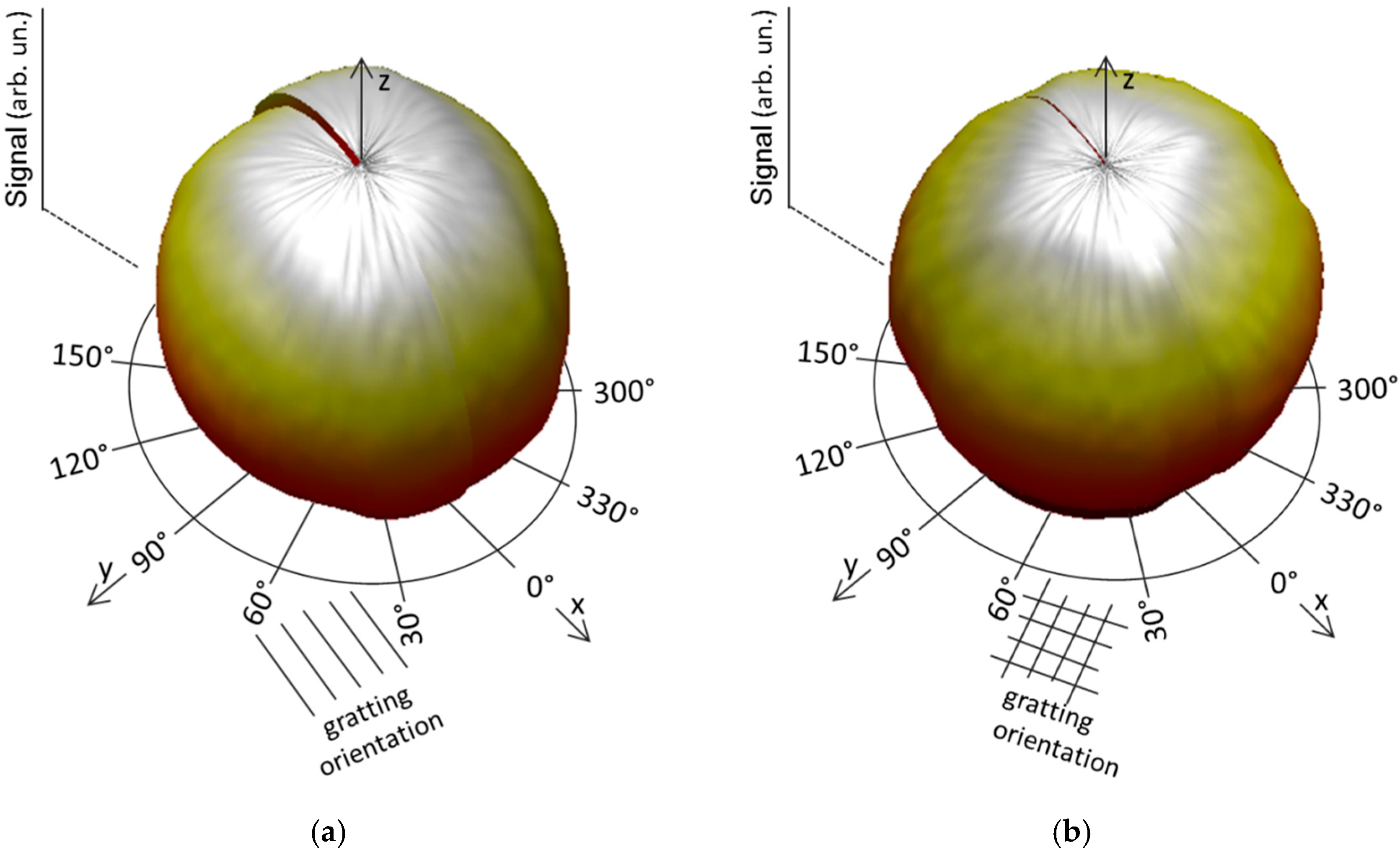
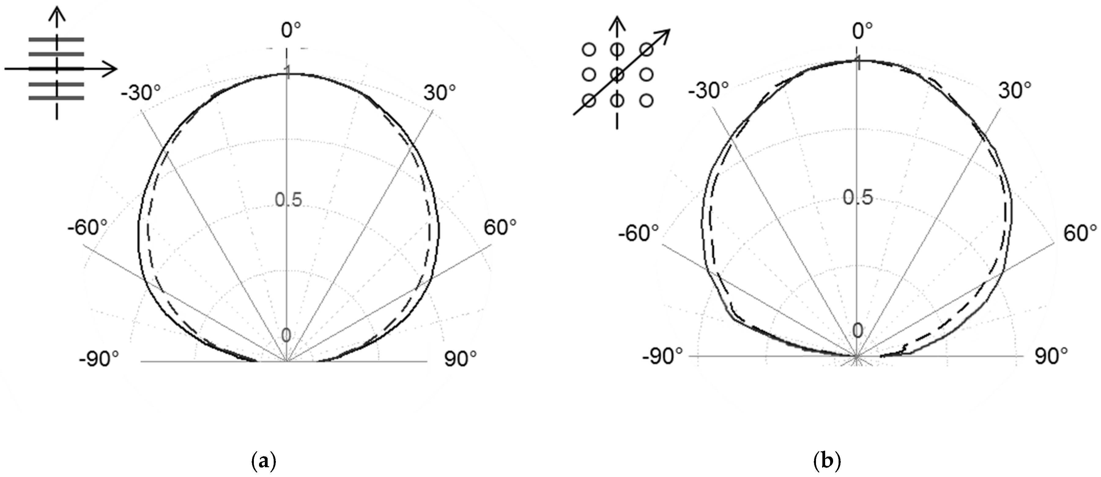
Radiation properties of LEDs were documented from far-field emissions measured by miniature goniophotometer. A Si detector rotated over the sample surface at a distance of 80 mm with 5° resolution of azimuthal and an elevation angle. The patterned LED surface modifies the Lambertian radiation diagram of conventional LEDs and creates spatial local extremes of light intensity due to the diffraction on the PhC gratings. The effect of the 1D PhC structure on the radiation pattern is shown in Figure 5a, creating local extremes in the direction across the structure grating. Diffraction extremes are not very sharp and are blurred because of the spectral width of the LED spectrum. Along the grating, there is no diffraction and the radiation pattern reflects the standard Lambertian diagram. The radiation pattern of 2D PhC shows evident diffraction on the 2D grating and forms a square symmetric radiation pattern as shown in Figure 5b.
This effect was studied in detail on vertical cross-sections of measured radiation patterns shown in Figure 6. While the 2D PhC LED with square symmetry produces the evident square radiation pattern, the 1D PhC structure does not show diffraction along the 1D surface grating and well reflects the reference LED. Weak diffraction extremes correspond to the first and second diffraction maximum with respect to the structure period in the defined direction. The diffraction extremes are calculated in Table 1. All the extremes presented were calculated for the emitting wavelength λ = 845 nm and can be found in the radiation patterns. Diffraction extremes are blurred around the calculated position because of spectral width of LED spectrum.
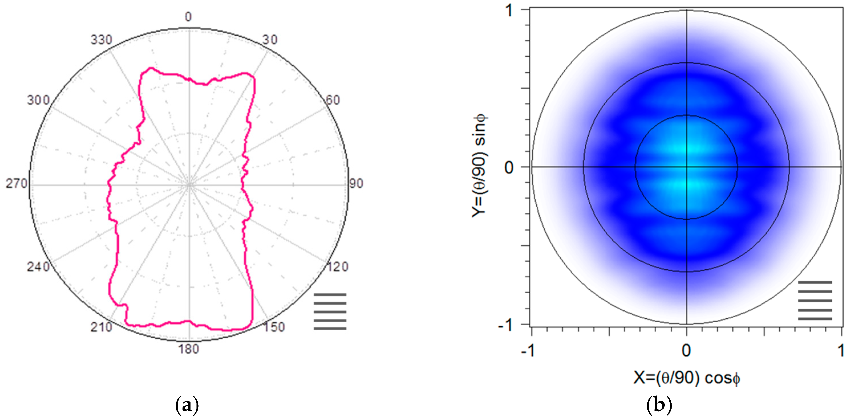
Generally, the diffraction effect in Figure 5 seems to be not so significant. It is caused by a strong background emission of LED close the contacts, where the surface LED was not patterned. These contact regions produce the Lambertian radiation pattern, which finally dominates in the measured radiation pattern. For an improved resolving of the structure effect on the diffraction properties, the radiation patterns were normalized with respect to the reference LED emission. Normalized radiation patterns shown in top view are compared with simulations of polar projections in Figure 7 for 1D grating and for 2D grating in Figure 8. In the normalized radiation patterns, both gratings form evident diffractions reflecting the structure symmetry. As shown in Figure 7a, the LED consisting of 1D grating forms the strong diffraction in the direction across the grating, while the 2D grating forms the square symmetrical radiation pattern in Figure 8a.
The simulations of optical properties of LEDs were performed by RSoft’s FullWAVE (version 6.3, Slovak University of Technologhy, Bratislava, Slovakia) which employs the well-known Finite-Difference Time–Domain (FDTD) technique. The optical field in the Beam Propagation Method (BPM) is shown in Figure 7b and Figure 8b. In the simulation, an approach was needed which automatically incorporates the necessary incoherent aspects and performs all the necessary pre- and post-processing to generate desired results, namely extraction ratio and radiation patterns. An unpolarized dipole source was created by the incoherent combination of three orthogonal dipoles. Then, the source in the active region of the LED is treated as a collection of single unpolarized point current sources. Spatial incoherence of these multiple sources is created by simulating each of these sources separately by FDTD, and the final incoherent result is the combination of those single coherent sources. Since the spatial incoherence time is usually thousands of time periods, this approach is a more efficient method than direct incoherent simulation by periodically randomizing the phases of the dipoles.
The simulation well reflects the real diffraction pattern of 1D and 2D PhC LEDs in Figure 7 and Figure 8. The small diffraction asymmetry of 2D PhC LED in Figure 7 could be caused by the slight structure asymmetry of irregular shape of patterned pillars shown in Figure 2b, which leads to different filling factors in normal directions. However, the simulations in Figure 7b and Figure 8b well coincide the optical field distribution of both 1D and 2D PhC structures patterned in the LED surface.
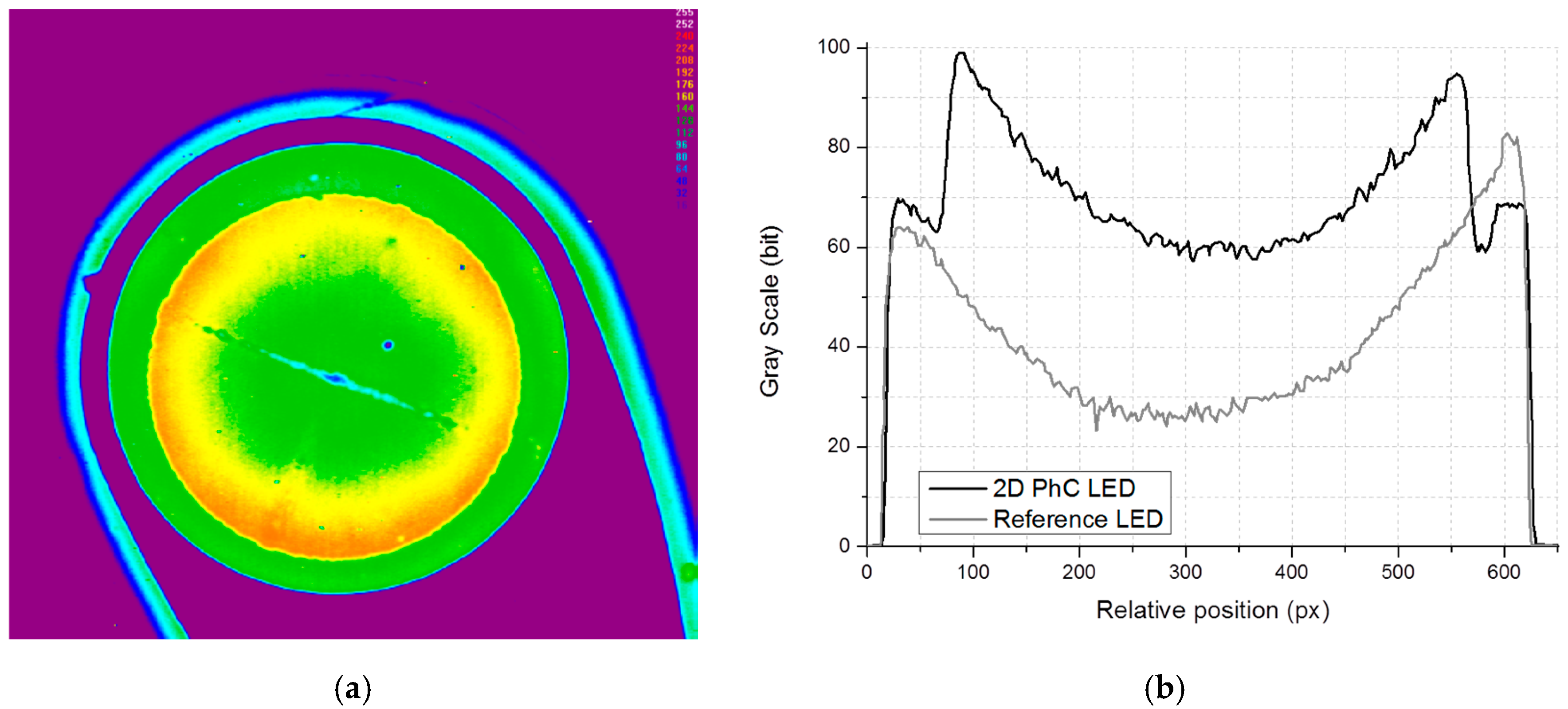
Much of the light generated in the active region never escapes the LED chip, because light-generation has a substantial refractive index mismatch on the semiconductor chip–air interface. The total internal reflection at the semiconductor chip–air interface means that most of the light remains confined to the LED chip. Obviously, this reduces the efficiency of LEDs. Additionally, GaAs-based LEDs creates high refractive index contrast on the semiconductor chip–air interface and produces light trapping. The crystal structuring of a different type leads to efficient light extraction in preferred directions. Structuring the top surface of the chip produces a regular two-dimensional array of holes or pillars called photonic crystals, which is now recognized as one of the most suitable techniques for extracting the horizontally-propagating trapped modes. The periodicity of metallic and semiconductor crystals interacts with the propagating wave and causes a diffraction and effective light extraction. The effect of the prepared 1D and 2D PhC in the LED surface was measured by L(I) dependencies in sphere with Si detector and compared with reference LED. As is shown in Figure 9, the 1D PhC produces a considerable increase of the surface emission with respect to the reference LED reaching 35%, while the 2D PhC shows app. 14% enhancement of the surface extraction. The surface enhancement is very promising, and moreover, it must be noted that the L(I) dependence presents the overall intensity enhancement including the unpatterned surface parts of LED. It was shown that just these parts contribute very dramatically to the overall emission. For the exact determination of the PhC structure contribution to the surface emission, the map of the surface emission was measured in Figure 10. The surface enhancement can be estimated from Figure 10b comparing the intensity of the 2D PhC LED and the reference LED in different patterned regions excluding the unpatterned regions close the contact. Some structures achieved the surface emission enhancement more than 110% as documented in the intensity map of the surface emission in Figure 10a measured at a current of 1 mA. The intensity profile in Figure 10b shows a doubled emission near the contacts provided by the nonhomogeneous lateral spreading of the current in the upper confinement layer. Regardless, the effect of the PhC is very significant and this analysis confirmed the unique light extraction from the surface of the patterned LED by PhC.
The period of presented structures was not optimized to the wavelength of emitting light. Optimized structure period related to the emission wavelength could lead to the next improvement of the properties in the near and far field.
4. Conclusions
This paper analyzes in detail the emission properties of AlGaAs/GaAs LEDs containing a 1D and 2D PhC structure with square symmetry and the same period. Homogeneous-patterned PhC structures of sufficient depth were confirmed from SEM analysis. Analysis in the near field and the diffraction properties determined from radiation pattern measurement documented that PhC-patterned LED works as an effective surface outcoupler of light produced in the active region while the surface emission dramatically increased from the patterned region. Results presented in this paper document the possibility of how to improve extraction efficiency, and modify the radiation pattern of the LEDs if the 1D and 2D PhC structure is patterned on the surface. The realized PhC LEDs show evident improvement of the light extraction efficiency based on light outcoupling on the patterned structure.
Author Contributions
Conceptualization, L.S. and D.P.; methodology, J.K.; software, A.K.; validation, D.P., J.S., and J.K.; formal analysis, J.S., L.S., and A.K.; investigation, L.S.; resources, J.S.; data curation, D.P.; writing—original draft preparation, D.P.; writing—review and editing, D.P. and L.S.; visualization, L.S.; supervision, J.K.J.; project administration, J.S.; funding acquisition, D.P. All authors have read and agreed to the published version of the manuscript.
Funding
This work was supported by the Slovak National Grant Agency under the project VEGA 1-0733/20 and the Slovak Research and Development Agency under the project No. APVV-16-0129.
Conflicts of Interest
The authors declare no conflict of interest.
References
- Hsieh, M.L.; Lo, K.C.; Lan, Y.S.; Yang, S.Y.; Lin, C.H.; Liu, H.M.; Kuo, H.C. One-shot exposure for patterning two-dimensional photonic crystals to enhance light extraction of InGaN-based green LEDs. IEEE Photonics Technol. Lett. 2008, 20, 141–143. [Google Scholar] [CrossRef]
- Xu, Z.; Cao, L.; Tan, Q.; He, Q.; Jin, G. Enhancement of the light output of light-emitted diode with double photonic crystals. Opt. Commun. 2007, 278, 211–214. [Google Scholar] [CrossRef]
- Adawi, A.M.; Kullock, R.; Turner, J.L.; Vasilev, C.; Lidzey, D.G.; Tahraoui, A.; Fry, P.W.; Gipson, D.; Smith, E.; Foden, C.; et al. Improving the light extraction efficiency of polymeric light emitting diodes using two-dimensional photonic crystals. Org. Electron. 2006, 7, 222–228. [Google Scholar] [CrossRef]
- Wierer, J.J.; Krames, M.R.; Epler, J.E.; Gardner, N.F.; Craford, M.G.; Wendt, J.R.; Simmons, J.A.; Sigalas, M.M. InGaN/GaN quantum-well heterostructure light-emitting diodes employing photonic crystal structures. Appl. Phys. Lett. 2004, 84, 3885–3887. [Google Scholar] [CrossRef]
- Cho, H.K.; Kim, S.K.; Bae, D.K.; Kang, B.C.; Lee, J.S.; Lee, Y.H. Laser liftoff GaN thin-film photonic crystal GaN-based Light-Emitting Diodes. IEEE Photonics Technol. Lett. 2008, 20, 2096–2098. [Google Scholar] [CrossRef]
- Mattioli, E.; Weisbuch, C. Impact of photonic crystals on LED light extraction efficiency: Approaches and limits to vertical structure designs. J. Phys. D Appl. Phys. 2010, 43, 354005. [Google Scholar] [CrossRef]
- Matioli, E.; Rangel, E.; Iza, M.; Fleury, B.; Pfaff, N.; Speck, J.; Hu, E.; Weisbuch, C. High extraction efficiency light-emitting diodes based on embedded air-gap photonic-crystals. Appl. Phys. Lett. 2010, 96, 031108. [Google Scholar] [CrossRef] [Green Version]
- Jiang, S.; Feng, Y.; Chen, Z.; Zhang, L.; Jiang, X.; Jiao, Q.; Li, J.; Chen, Y.; Li, D.; Liu, L.; et al. Study on light extraction from GaN-based green light-emitting diodes using anodic aluminum oxide pattern and nanoimprint lithography. Sci. Rep. 2016, 6, 21573. [Google Scholar] [CrossRef] [Green Version]
- Charlton, M.D.B.; Shields, P.A.; Allsop, D.W.E.; Wang, W.N. High-efficiency photonic quasi-crystal light emitting diodes incorporating buried photonic crystal structures. In Proceedings of the Tenth International Conference on Solid State Lighting, San Diego, CA, USA, 1–5 August 2010; Volume 7784, p. 778407. [Google Scholar] [CrossRef]
- Husanu, M.A.; Ganea, C.P.; Anghel, I.; Florica, C.; Rasoga, O.; Popescu, D.G. Surface topography to reflectivity mapping in two-dimensional photonic crystals designed in germanium. Appl. Surf. Sci. 2015, 355, 1186–1191. [Google Scholar] [CrossRef]
- Lee, Y.J.; Kim, S.H.; Kim, G.H.; Lee, Y.H.; Cho, S.H.; Song, Y.W.; Kim, Y.C.; Do, Y.R. Far-field radiation of photonic crystal organic light—emitting diode. Opt. Express 2015, 13, 5864–5870. [Google Scholar] [CrossRef] [Green Version]
- Gong, H.; Hao, X.; Wu, Y.; Cao, B.; Xia, W.; Xu, X. Enhanced light extraction from GaN-based LEDs with a bottom-up assembled photonic crystal. Mater. Sci. Eng. B 2011, 176, 1028–1031. [Google Scholar] [CrossRef]
- Khokhar, A.Z.; Parsons, K.; Hubbard, G.; Watson, I.M.; Rahman, F.; Macintyre, D.S.; Xiong, C.; Massoubre, D.; Gong, Z.; Gu, E.; et al. Emisson characteristics of photonic crystral light-emitting diodes. Appl. Opt. 2011, 50, 3233–3239. [Google Scholar] [CrossRef] [Green Version]
- Zhang, P.; Wen, Q.; Xu, X. Parameters optimization of nanopatterned sapphire substrates for enhancing light extraction efficiency of GaN-based LEDs. Opt. Commun. 2020, 464, 125548. [Google Scholar] [CrossRef]
- Charlton, M.D.B.; Zoorob, M.E.; Lee, T. Photonic quasi-crystal LEDs, design, modelling, and optimization. In Light-Emitting Diodes: Research, Manufacturing, and Applications XI, Proceedings of the Integrated Optoelectronic Devices; SPIE: San Jose, CA, USA, 20–25 January 2007; Volume 6486, pp. 64860R1–64860R10. [Google Scholar] [CrossRef] [Green Version]
- Campbell, M.; Sharp, D.N.; Harrison, M.T.; Denning, R.G.; Turberfield, A.J. Fabrication of photonic crystals for the visible spectrum by holographic lithography. Nature 2000, 404, 53–56. [Google Scholar] [CrossRef] [PubMed]
- Suslik, L.; Pudis, D.; Goraus, M.; Nolte, R.; Kovac, J.; Durisova, J.; Gaso, P.; Hronec, P.; Schaaf, P. Photonic crystal and photonic quasicrystal patterned in PDMS surfaces and their effect on LED radiation properties. Appl. Surf. Sci. 2017, 395, 220–225. [Google Scholar] [CrossRef]
- Urbancova, P.; Pudis, D.; Kuzma, A.; Goraus, M.; Gaso, P.; Jandura, D. IP-Dip-based woodpile structures for VIS andNIR spectral range: Complex PBG analysis. Opt. Mater. Express 2019, 9, 4307–4317. [Google Scholar] [CrossRef]
- Lai, N.D.; Liang, W.P.; Lin, J.H.; Shu, C.C.; Lin, C.H. Fabrication of two- and three-dimensional periodic structures by multi-exposure of two beam interference technique. Opt. Express 2005, 13, 9605–9611. [Google Scholar] [CrossRef] [PubMed]
- Mikulskas, I.; Mickevičius, J.; Vaitkus, J.; Tomašiunas, R.; Grigaliunas, V.; Kopustinskas, V.; Meškinis, Š. Fabrication of photonic structures by means of interference lithography and reactive ion etching. Appl. Surf. Sci. 2002, 186, 599–603. [Google Scholar] [CrossRef]
- Quinonez, F.; Menezes, J.W.; Cescato, L.; Rodriguez-Esquerre, V.F.; Hernandez-Figueroa, H.; Mansano, R.D. Band gap of hexagonal 2D photonic crystals with elliptical holes recorded by interference lithography. Opt. Express 2006, 14, 4873–4879. [Google Scholar] [CrossRef] [PubMed] [Green Version]
- Zhang, X.; Liu, S.; Liu, Y.; Chen, X.; Lin, H.; Ren, X. Enhancement of LED light extraction via diffraction of hexagonal lattice fabricated in ITO layer with holographic lithography and wet etching. Phys. Lett. A 2008, 372, 3738–3740. [Google Scholar] [CrossRef]
- Kubicova, I.; Pudis, D.; Suslik, L.; Skriniarova, J. Spatial resolution of apertureless metal-coated fiber tip for NSOM lithography determined by tip-to-tip scan. Optik 2013, 124, 1971–1973. [Google Scholar] [CrossRef]
- Steingrüber, R.; Golka, S.; Heidrich, H. Useful and costefficient fabrication of dot arrays for photonic crystals by direct-write electron-beam lithography. Microelectron. Eng. 2003, 67, 157–161. [Google Scholar] [CrossRef]
- Hronec, P.; Pudis, D.; Skriniarova, J.; Kovac, J.; Andok, R. Lithographic technologies suitable for PhC patterning and optical properties of patterned LED surfaces. Optik 2017, 143, 35–41. [Google Scholar] [CrossRef]
Figure 1.
SEM image of AlGaAs/GaAs MQW LED patterned surface with photonic structure in the emitting part of the LED surface.
Figure 1.
SEM image of AlGaAs/GaAs MQW LED patterned surface with photonic structure in the emitting part of the LED surface.

Figure 2.
(a) SEM detail of 1D PhC structure and (b) SEM image of 2D pillar structure arranged in 2D square symmetry with period of 700 nm.
Figure 2.
(a) SEM detail of 1D PhC structure and (b) SEM image of 2D pillar structure arranged in 2D square symmetry with period of 700 nm.

Figure 3.
(a) Image of the near field of LED patterned with 1D PhC structure and (b) corresponding NSOM line profile across the structure.
Figure 3.
(a) Image of the near field of LED patterned with 1D PhC structure and (b) corresponding NSOM line profile across the structure.

Figure 4.
(a) Image of the near field of LED patterned with 2D PhC structure and (b) corresponding NSOM line profile across the structure.
Figure 4.
(a) Image of the near field of LED patterned with 2D PhC structure and (b) corresponding NSOM line profile across the structure.

Figure 5.
(a) 3D radiation pattern of 1D PhC LED and (b) 2D PhC LED with the same period of 700 nm.

Figure 6.
(a) Comparison of radiation pattern diagram of LED with 1D PhC and (b) 2D PhC measured at two different directions.
Figure 6.
(a) Comparison of radiation pattern diagram of LED with 1D PhC and (b) 2D PhC measured at two different directions.

Figure 7.
(a) Normalized radiation pattern shown as a contour graph for the selected constant intensity and (b) the polar projection of the simulated far field of 1D PhC LED.
Figure 7.
(a) Normalized radiation pattern shown as a contour graph for the selected constant intensity and (b) the polar projection of the simulated far field of 1D PhC LED.

Figure 8.
(a) Normalized radiation pattern shown as a contour graph for the selected constant intensity and (b) the polar projection of the simulated far field of 2D PhC LED.
Figure 8.
(a) Normalized radiation pattern shown as a contour graph for the selected constant intensity and (b) the polar projection of the simulated far field of 2D PhC LED.

Figure 9.
L(I) dependence of LEDs with 1D PhC and 2D PhC structures compared with reference LED.

Figure 10.
(a) Intensity image of surface emission LED with 2D PhC structure and (b) its profile compared with reference LED.
Figure 10.
(a) Intensity image of surface emission LED with 2D PhC structure and (b) its profile compared with reference LED.


Table 1.
Diffraction extremes for 1D and 2D PhC structure calculated for different directions and for first three diffraction orders. Direction 45° corresponds to diagonal of square grating.
Table 1.
Diffraction extremes for 1D and 2D PhC structure calculated for different directions and for first three diffraction orders. Direction 45° corresponds to diagonal of square grating.
| Structure/Diffraction Order | 1st | 2nd | 3rd |
|---|---|---|---|
| 1D PhC (700 nm)/0° | 22.8 | 50.8 | – |
| 2D PhC (700 nm)/0° | 22.8 | 50.8 | – |
| 2D PhC (700 nm)/45° | 15.9 | 33.2 | 55.3 |
© 2020 by the authors. Licensee MDPI, Basel, Switzerland. This article is an open access article distributed under the terms and conditions of the Creative Commons Attribution (CC BY) license (http://creativecommons.org/licenses/by/4.0/).
Share and Cite
MDPI and ACS Style
Suslik, L.; Skriniarova, J.; Kovac, J.; Pudis, D.; Kuzma, A.; Kovac, J., Jr. Complex Analysis of Emission Properties of LEDs with 1D and 2D PhC Patterned by EBL. Coatings 2020, 10, 748. https://doi.org/10.3390/coatings10080748
AMA Style
Suslik L, Skriniarova J, Kovac J, Pudis D, Kuzma A, Kovac J Jr. Complex Analysis of Emission Properties of LEDs with 1D and 2D PhC Patterned by EBL. Coatings. 2020; 10(8):748. https://doi.org/10.3390/coatings10080748
Chicago/Turabian StyleSuslik, Lubos, Jaroslava Skriniarova, Jaroslav Kovac, Dusan Pudis, Anton Kuzma, and Jaroslav Kovac, Jr. 2020. "Complex Analysis of Emission Properties of LEDs with 1D and 2D PhC Patterned by EBL" Coatings 10, no. 8: 748. https://doi.org/10.3390/coatings10080748
Note that from the first issue of 2016, this journal uses article numbers instead of page numbers. See further details here.