Atomic Layer Deposition of Superconducting CuO Thin Films on Three-Dimensional Substrates


1
Institute of Physics, University of Tartu, W. Ostwaldi 1, 50411 Tartu, Estonia
2
Department of Chemistry, Lomonosov Moscow State University, Leninskie Gory 1-3, 119991 Moscow, Russia
3
National Institute of Chemical Physics and Biophysics, Akadeemia Tee 23, 12618 Tallinn, Estonia
*
Author to whom correspondence should be addressed.
Crystals 2020, 10(8), 650; https://doi.org/10.3390/cryst10080650
Submission received: 19 June 2020
/
Revised: 27 July 2020
/
Accepted: 28 July 2020
/
Published: 29 July 2020
(This article belongs to the Special Issue Advances in Thin Film Materials and Devices)
Abstract
:In previous decades, investigation of superconductors was aimed either at finding materials with higher critical temperatures or at discovering nontypical superconducting behavior. Here, we present the cupric (CuO) thin films, which were synthesized by atomic layer deposition by using a metal-organic precursor, copper (II)-bis-(-dimethylamino-2-propoxide), and ozone as an oxidizer. The deposition process was optimized by employing a quartz crystal monitoring, and the contact between the deposited films and planar and three-dimensional SiO2/Si substrates was examined by scanning electron microscopy with a focused ion beam module. Phase and elemental composition were analyzed by X-ray diffraction and X-ray fluorescence. Two-probe electrical resistivity measurements revealed a resistivity drop below the critical temperature of 4 K, which may indicate low-temperature superconductivity of the CuO thin films.
1. Introduction
Even since the first discovery of superconductivity [1], investigation of superconductors was aimed either at finding materials with higher critical temperatures Tc or, later, at discovering unconventional superconducting behavior, which significantly deviates from the conventional Bardeen-Cooper-Schrieffer model [2]. Over recent decades, several exotic superconductor-families based on copper, iron, hydrogen, carbon, and even nickel have been discovered and explored. More or less complex copper oxides, cuprates, are endowed with a unique combination of features that make them excellent magnetic model systems and/or good superconductors. First, the 3d9 electronic configuration of Cu2+ ensures the absence of the charge degrees of freedom. Second, sizable Jahn-Teller distortions are typical of Cu2+; they stabilize an ordered orbital ground state. Thus, the low-energy physics of cuprates is driven by the magnetic degrees of freedom due to S = 1/2 spins localized on Cu2+ atoms. The variety of spin lattices found in cuprates is ensured by their unique structural diversity and initially stimulated the discovery of high-temperature superconductivity in cuprate oxides [3].
Two well-known and most common binary oxides of copper, cuprous (Cu2O) and cupric (CuO) oxide, have been synthesized or modeled, and studied in many works. The oxidation and corrosion of copper, particularly as seen by the surface science, was recently reviewed by Gattinoni and Michaelides [4]. It was shown that the formation of copper oxides proceeds either epitaxially or, in most cases, through the formation of nano-islands, which grow and eventually coalesce under the exposure of oxygen, resulting in continuous thin solid films. Cu2O possesses moderate electron mobility, and the Cu2O films, epitaxially grown on MgO by pulsed laser deposition, were examined as thin film transistor channels [5]. The formation of interconnecting Cu bias between transistors in a computing processor can be made by the initial growth of Ru-doped Cu2O films, followed by their reduction to Cu [6]. Cu2O films were studied also as photoconductive materials [7,8]. Notably, CuO was investigated as a prototype multiferroic material, owing to its hidden magnetoelectric properties [9,10]. The cupric oxide CuO is the only known binary multiferroic [8] with the notably high transition temperature in the multiferroic state, 230 K, and with a quite rich and interesting high-field phase diagram [11].
Thin films, consisting of nanocrystals of CuO, Cu2O and mixed CuO/Cu2O phases, obtained by wet chemical synthesis, exhibit chemical sensing properties [12]. Furthermore, Cu2O nanocrystallites may be considered as an effective catalyst in the oxidation of carbon monoxide to carbon dioxide [13]. Cu2O itself can actually be reduced from CuO films upon vacuum annealing [14]. Room-temperature ferromagnetism was observed in structurally defective, nonstoichiometric, porous Cu2O films deposited by sputtering [15].
The growth of copper oxide films by atomic layer deposition (ALD) was reported to yield Cu2O as the main phase when using, for instance, (n-Bu3P)2Cu(acac) and O2, in the temperature range of 22–300 °C [16]; bis(1-dimethylamino-2-methyl-2-butoxy)copper, (C14H32N2O2Cu), and H2O in the temperature range of 120–240 °C [17]; (II)-bis-(dimethylamino-2-propoxide)copper, Cu(dmap)2 and H2O in the temperature range of 110–200 °C [18]. Cu2O nanodots also have been grown by ALD on sapphire from (C14H32N2O2Cu) and H2O at 140 °C [19]. In a very recent study, Cu2O growth by ALD has been explored by using copper (II) acetate, Cu(OAc)2, and H2O as precursors [8].
In the form of CuO, copper oxide films were grown by ALD from Cu(dmap)2 and O3 in the temperature range of 80–140 °C [7,20], and from Cu(thd)2 and O3 in the temperature range of 200–260 °C [21]. Cu2O1.25 films were grown at 100 °C by plasma-enhanced ALD, where the phase-selective formation of CuO, Cu2O, and Cu films, as claimed, has been performed by controlling the number of Cu deposition steps in one deposition cycle [22].
Various Cu precursors, such as copper(I)-N,N′-di-sec-butyl-acet-amidinate, copper(I)-N-sec-butyl-2-iminopyrrolidinate, and copper(I)-N-tert-butyl-5,5-dimethyl-2-imino- pyrrolidinate, were investigated in terms of their initial adsorption on silicon oxide surfaces, potentially useful in ALD processes [23].
In the present work, we report on atomic layer deposition of the CuO thin films by using the copper (II)-bis-(dimethylamino-2-propoxide) and ozone as precursors on planar and 3D stack type substrates (i.e., Si substrates having a regular pattern of vertical etched channels with the depth of ~1.5 μm). We investigated phase composition of the deposited films by conventional X-ray diffraction and examined the structure of the films depending on the deposition conditions. Physical properties of the deposited films are characterized by means of low-temperature electrical resistivity measurements.
2. Materials and Methods
The cupric oxide films were grown in a low-pressure (200–260 Pa) flow-type in-house-built hot-wall ALD reactor (Tartu, Estonia). Copper(II)-bis-(dimethylamino-2-propoxide), Cu(dmap)2, was evaporated at the temperatures ranging from 81 to 87 °C. Ozone was produced from O2 (99.999% purity, AGA) using a BMT Messtechnik 802 N generator (Frankfurt, Germany for all suppliers, manufacturers, and software companies. Please review and revise throughout the The ozone concentration, measured by BMT Messtechnik 964 analyzer (Germany) for all suppliers, manufacturers, and software companies. Please review and revise throughout the, was 200–220 g/m3 in our experiments. The partial pressure of oxygen precursor was 34 Pa in the reaction chamber during the O3/O2 pulse. Quartz crystal monitoring (QCM) was applied to establish the evaporation and substrate temperature ranges, enabling effective evaporation of the precursor and the deposition of the target material. QCM data were acquired by Q-pod monitor (Inficon, Switzerland) for all suppliers, manufacturers, and software companies. Please review and revise throughout the) from an AT-cut quartz crystal (IQD Microprocessor Crystal) with the initial oscillation frequency of 6 MHz. As the variations of mass sensor temperature notably influence the QCM signal, real-time studies were performed at the substrate temperature between 112 and 165 °C. The best results were achieved at 140 °C. These studies revealed that the application of reduced amount of O3 may efficiently improve the deposition of target CuO films.
After determining the reactor conditions allowing the growth of CuO films, the solid films were deposited by using 500, 2000, 5000, and 10,000 deposition cycles with cycle times 2-2-2-5 s, for the cycle sequence Cu(dmap)2 pulse–purge–O3 pulse–purge. Before the depositions, Si (100) substrate was rinsed in a mixture of H2SO4:H2O2 (ratio 5:2) and heated on a hot plate at 80 °C. After that, Si (100) was washed with distilled water in an ultrasonic cleaner. In the next step, the samples were cleaned with a 7% solution of HF and washed again with distilled water in an ultrasonic bath. After cleaning and before placing the substrates in a reactor, a few nm thin film of SiO2 is formed on the substrate surface because of the contact with surrounding air. Three-dimensional stack substrates were cleaned only with distilled water.
The crystal structure of the grown films was evaluated by grazing incidence X-ray diffractometry (GIXRD), by using a Rigaku SmartLab X-ray diffractomete -r with CuKα radiation (X-ray wavelength of 0.15406 nm) and PDXL software for primary structural analysis. The same equipment was used for X-ray reflectometry (XRR) to estimate the thickness of the films. The surface morphology of planar films and 3D stacks (both bird-eye and cross-section images) was evaluated by scanning electron microscopy (SEM), by using a Dual Beam equipment with a focused ion beam (FIB) module and an Omniprobe model 100.7 in-situ nanomanipulator (FEI Helios NanoLab 600, Instead of using FIB for creating cross-sections of the samples where thin film was deposited into 3D substrates, the breaking of the samples into half before measurements was preferred, in order to avoid possible influence of the FIB to the 3D stacks (mainly amorphization). Other advantages of breaking the sample into half prior to measurements without using FIB are: the sample preparation speed, possibility to investigate larger areas compared to the regular FIB created cross-sections, and a lack of need for the deposition of a protective (Pt) layer. Some of the disadvantages are poorer control over the location of breakage/cross section area and the roughness of the cross-section area due to uncontrollable crack formation. An X-ray fluorescence (XRF) spectrometer (Rigaku ZSX 400) with the software program ZSX (version 5.55) was used to evaluate the elemental composition and mass thickness of the layer.
For electrical resistivity measurements, the standard four-probe technique was used. Four electrical contacts (Cu wires with the diameter of 100 μm) were attached to the film by using silver-containing epoxy resin. Typical distance between the neighboring probes was 250 μm. In the four-probe configuration, electrical current in the range between 40 nA and 10 mA was tested, yielding no registered voltage due to the high electrical resistance of the film at room temperature. Thus, the standard four-probe measurements are not possible, and the resistivity was measured by the two-probe method by using the neighboring contacts as voltage and current probes. In the two-probe measurements, the electrical current of 4.2 μA was used for the distance between probes of 265 μm. Electrical resistivity was measured using the Resistivity option of a Physical Property measurement System (PPMS, Quantum Design, San Diego, CA, USA) at temperatures between 1.8 K and 300 K in zero applied magnetic field (H = 0 T). The empty Si substrate was measured at temperatures between 250 K and 400 K as a reference sample.
3. Results and Discussion
The QCM sensor signal was recorded, first, as a function of Cu(dmap)2 pulse duration and, second, as a function of O3 pulse duration (Figure 1), in order to determine the appropriate doses of Cu(dmap)2 and O3. This measurement was performed to find the temperatures for surface reactions, which lead to the formation of CuO film with excess of oxygen. These conditions should be sufficient to form a film, but, at the same time, they should not be too stable to form cuprous oxide, Cu2O. It has been shown that the formation of copper oxides proceeds either epitaxially or, in most cases, under the exposure of oxygen (not ozone), resulting in continuous thin solid films [8]. In the case when the O3 cycle times were too long (twice longer than the metal precursor), the Cu2O film was formed [7,20].
According to the XRF analysis of the films grown by using 500 ALD cycles, the atomic ratio of copper to oxygen reached the values of 1.06 ± 0.07, 1.20 ± 0.08, and 1.19 ± 0.19 in the films grown at 112, 140, and 165 °C, respectively. The results imply that the CuO is the preferred copper oxide phase in the chosen temperature range. The content of residual carbon was found to be 15.4 ± 0.4, 9.0 ± 0.6 and 25.4 ± 0.8 mass % in the films grown at 112, 140, and 165 °C, respectively. This was indicative of the preferred substrate temperature around 140 °C in order to provide films with the highest purity under particular reactor conditions. Therefore, in further experiments, the substrate temperature was held at 140 °C.
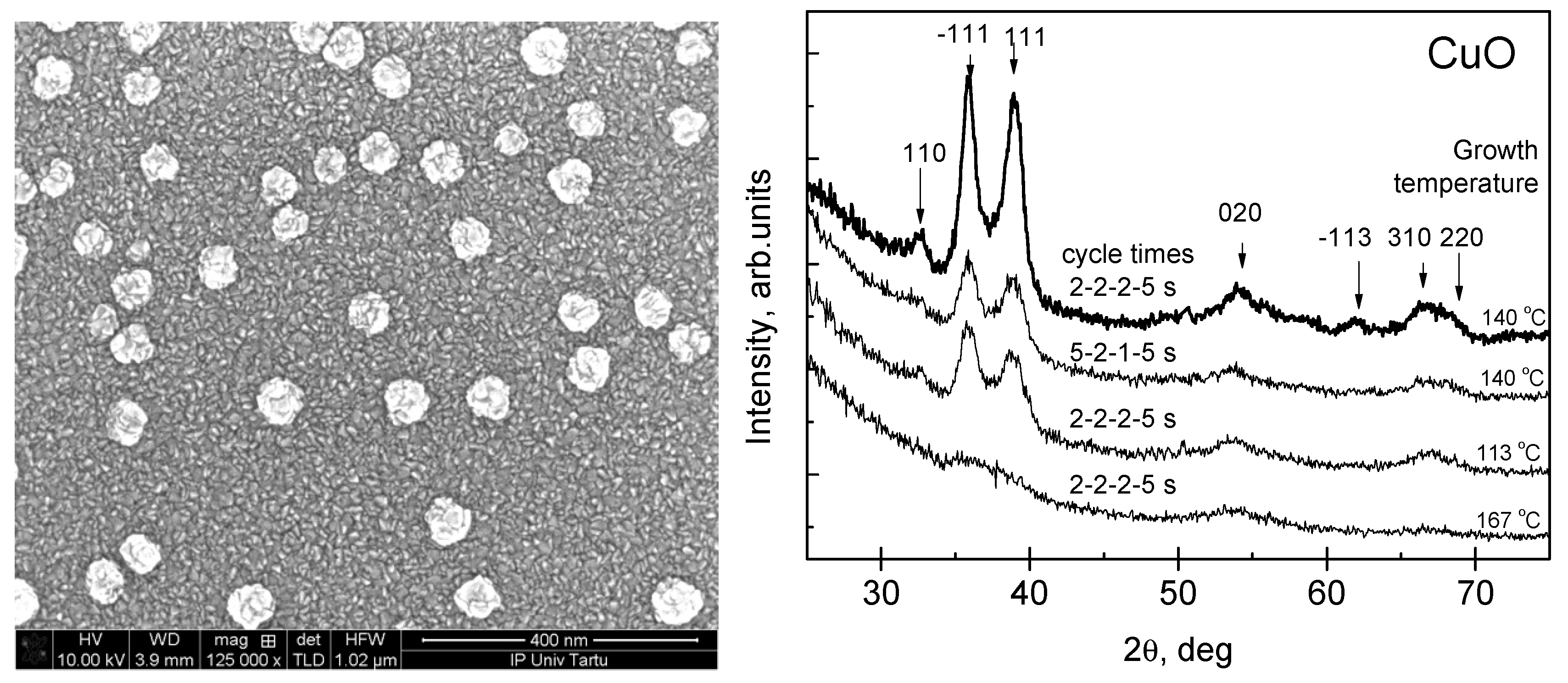
Figure 2 presents the thin CuO film grown by using 500 deposition cycles. The light features on the SEM images possibly correspond to the regions of lower conductivity (Figure 2, left panel). Previously, it was shown that charging/discharging effects for nonconductive/conductive areas of the specimen affect the SEM image intensity [24]. Based on the XRF analysis, one could decide that these areas can be caused by an excess copper on top of the film. However, the spots disappeared when more ALD cycles were performed.
The GIXRD patterns from the films deposited by using 500 cycles (cycle times 2-2-2-5 s) showed strong reflections at 32.5, 35.5, 38.8, 53.6, 66.5, and 68.1 deg, indicating the presence of CuO (PDF 01-073-6023) (Figure 2, right panel). In the case, when the metal precursor cycle times were too long (five time longer than the oxidizer precursor, 5-2-1-5 s), or the films were deposited at lower temperatures (113 °C) or higher temperatures (167 °C), the crystallinity of films was significantly reduced (Figure 2, right panel).
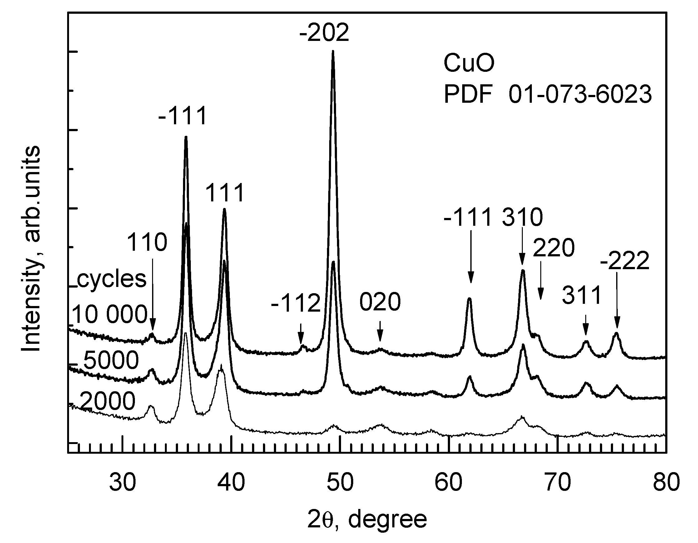
Table 1 and Figure 3 present the GIXRD and XRR results of a structural analysis of deposited films by using a different number of ALD cycles. The thickest film was continuous and crystallized in the CuO phase.
Analysis of phase composition by XRD clearly shows that the CuO oxide is the main phase in copper oxide films. It is worth noting, that the appearance of a dominant CuO is highly desirable when one aims at superconducting materials, which are applicable, for instance, in quantum computing. In particular, the achievement of [111] orientation in nanocrystalline thin films of the electron-doped cuprate materials would be necessary for this purpose, as mentioned by Kang et al., where superconducting behavior has been observed in Nd2CuO single crystals [25].
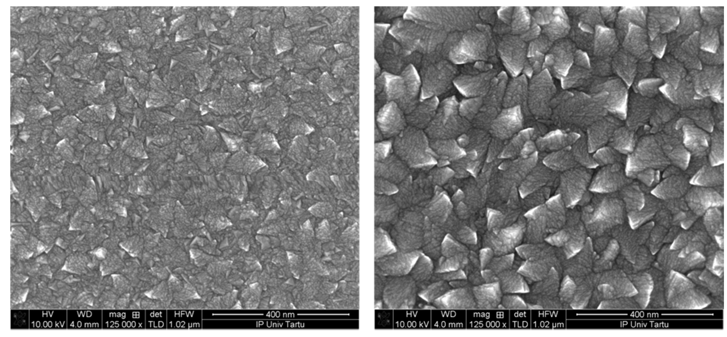
The morphology of CuO films depends on the number of cycles used, the films deposited after 5000 and 10,000 cycles are shown in Figure 4. As could be expected, the grain size and the thicknesses of the films increase with increasing the number of cycles. However, it is noteworthy, that, even in the case of large number of deposition cycles, the coverage of three-dimensional substrates with the aspect ratio of 1:20 is appreciable. In contrast to Si (111) substrates, a three-dimensional substrate is not planar having etched vertical channels perpendicular to the surface. Such 3D substrates are typically used to investigate the filling of pores by the film material. Even if pores seem to be closed above the wafer level during the growth process (Figure 5), some film material was deposited inside the pores, too. Certain stage coverage becomes important when one aims at coating the arbitrarily shaped nanostructures with the functional films used in applications. Good conformality and discontinuity on highly trenched substrates were achieved previously for Cu2O films [26] but not for CuO films. For example, in most of quantum-computer-related nanostructures, alumina was used as the electrode material. However, the deposition of metals on more complicated substrates remains a challenging task, as discussed by Gazibegovic et al. [27].
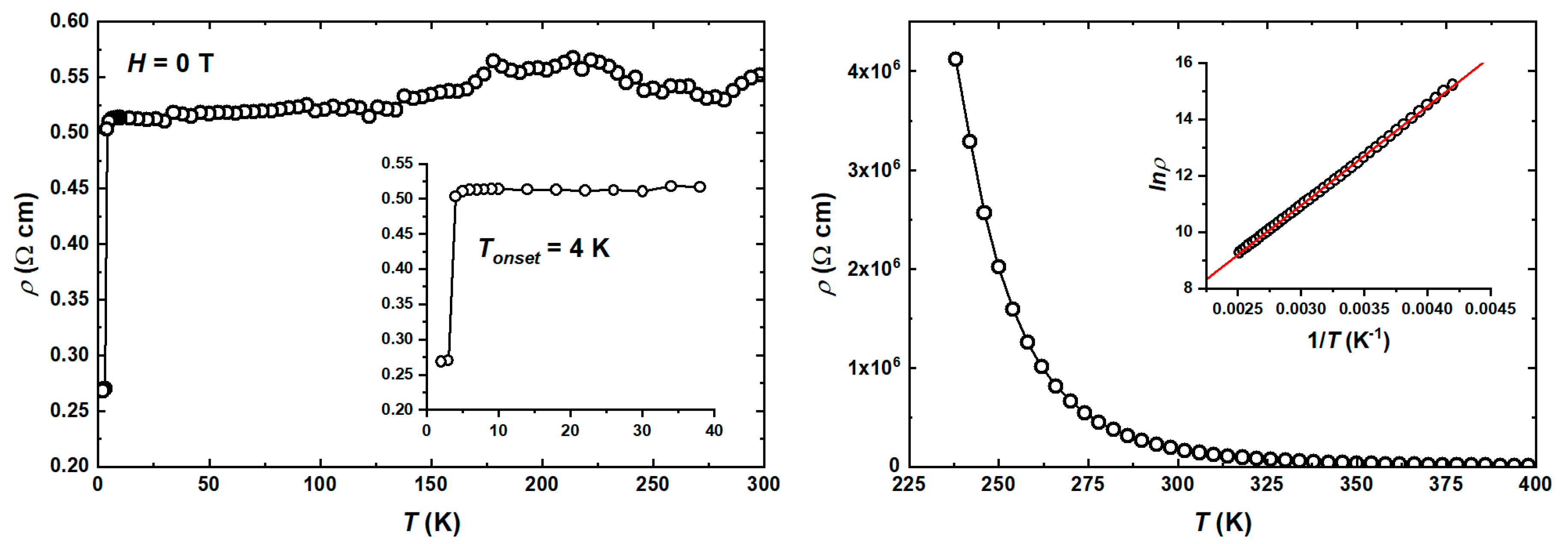
Electrical resistivity of the CuO film was examined by two-probe technique in zero applied magnetic field. Giving that the two-probe measurements may contain artifacts due to the additional contribution from electrical contacts, the reproducibility of measurements was checked. The two-probe measurements were found fully reproducible, and the representative results are shown in Figure 6. The resistivity of CuO film is 0.55 Ω cm at room temperature, and almost temperature-independent in the temperature range of 10–300 K. The CuO films produced using other methods, such as sputtering, possess the resistivity values of 0.1–800 Ω cm depending on film thickness and deposition conditions, such as oxygen partial pressure and whether the direct current or radio frequency sputtering, was applied according to the previous reports [28]. In the present study, at low temperatures, the drop of resistivity was detected at the onset temperature of Tonset = 4 K. The resistivity was abruptly reduced by 50% reaching the value of ~0.27 Ω cm at T = 2 K (Figure 6 left panel). Such drop in the resistivity can be related to the fact that a part of the CuO film becomes superconducting under cooling. However, other scenarios are also possible, including poor electrical contact because of the film shrinkage under cooling or due to the mismatch between thermal expansion coefficients of the film and substrate. In the reference measurement, we probed the electrical resistance of an empty Si substrate without CuO film. The resistivity of Si substrate is notably higher than the resistivity of CuO film and exhibits the activation behavior (Figure 6, right panel), which is shown as a linear fit of the lnρ vs. 1/T data in the inset of Figure 6 (right panel, inset). Possible superconductivity of the CuO films unveiled in this study requires further detailed investigation. In quantum-computer-related nanostructures, where Al was used (TC = 1.2 K) as electrode material [28], the use of CuO films on complicated 3D structures instead of Al may increase the working temperature and make the system more controllable at low temperatures.
4. Conclusions
In summary, we investigated halide-free atomic layer deposition technique for crystalline and stoichiometric CuO films. The films were deposited using Cu(dmap)2 and O3 as precursors, and the growth rate was 0.02 nm per cycle at 140 °C. To achieve the CuO phase instead of Cu2O, the process was controlled with QCM and XRD. The influence of the metal precursor temperature, as well as of the length of the precursors cycle times, was evaluated and the conditions for deposition of CuO on stacked 3D substrates were established. The electrical properties of CuO films at low temperatures were investigated, and the sharp drop of resistivity was detected at Tonset = 4 K in zero applied magnetic field. This drop of resistivity can be due to superconductivity of the CuO film, which requires further studies. The future investigation should be focused on the interrelations between grain size, lattice constant, phase composition, and critical temperature of the resistivity drop on the thickness of CuO films prepared by atomic layer deposition.
Author Contributions
Conceptualization, methodology and writing—original draft preparation, A.T. (Aile Tamm); preparation and characterization, A.T. (Aivar Tarre), formal analysis, H.S.; resistivity measurements and writing, V.V. and R.S. All authors have read and agreed to the published version of the manuscript.
Funding
This work was funded by the European Regional Development Fund project TK134 “Emerging orders in quantum and nanomaterials” and Estonian Research Agency project PRG4 “Emerging novel phases in strongly frustrated quantum magnets”.
Acknowledgments
We thank K. Kukli for encouraging conversations about the chemistry of precursors.
Conflicts of Interest
The authors declare no conflict of interest.
References
- Onnes, H.K. The disappearance of the resistivity of mercury. Comm. Leiden 1911, 122, 2. [Google Scholar]
- Bardeen, J.; Cooper, L.N.; Schrieffer, J.R. Theory of Superconductivity. Phys. Rev. 1957, 108, 1175–1204. [Google Scholar] [CrossRef] [Green Version]
- Bednorz, J.G.; Müller, K.A. Possible high Tc superconductivity in the Ba-La-Cu-O system. Z. Phys. B Condens. Matter 1986, 64, 189–193. [Google Scholar] [CrossRef]
- Gattinoni, C.; Michaelides, A. Atomistic details of oxide surfaces and surface oxidation: The example of copper and its oxides. Surf. Sci. Rep. 2015, 70, 424–447. [Google Scholar] [CrossRef] [Green Version]
- Matsuzaki, K.; Nomura, K.; Yanagi, H.; Kamiya, T.; Hirano, M.; Hosono, H. Epitaxial growth of high mobility Cu2O thin films and application to p-channel thin film transistor. Appl. Phys. Lett. 2008, 9, 202107. [Google Scholar] [CrossRef]
- Dhakal, D.; Assim, K.; Lang, H.; Bruener, P.; Grehl, T.; Georgi, C.; Waechtler, T.; Ecke, R.; Schulz, S.E.; Gessner, T. Atomic layer deposition of ultrathin Cu2O and subsequent reduction to Cu studied by in situ x-ray photoelectron spectroscopy. J. Vac. Sci. Technol. A 2016, 34, 01A111. [Google Scholar] [CrossRef]
- Iivonen, T.; Hämäläinen, J.; Marchand, B.; Mizohata, K.; Mattinen, M.; Popov, G.; Kim, J.; Fischer, R.A.; Leskelä, M. Low-temperature atomic layer deposition of copper(II) oxide thin films. J. Vac. Sci. Technol. A 2016, 34, 01A109. [Google Scholar] [CrossRef]
- Iivonen, T.; Heikkilä, M.J.; Popov, G.; Nieminen, H.-E.; Kaipio, M.; Kemell, M.; Mattinen, M.; Meinander, K.; Mizohata, K.; Räisänen, J.; et al. Atomic layer deposition of photoconductive Cu2O thin films. ACS Omega 2019, 4, 11205–11214. [Google Scholar] [CrossRef] [Green Version]
- Jones, S.P.P.; Gaw, S.M.; Doig, K.I.; Prabhakaran, D.; Wheeler, E.M.H.; Boothroyd, A.; Lloyd-Hughes, J. High-temperature electromagnons in the magnetically induced multiferroic cupric oxide driven by intersublattice exchange. Nat. Commun. 2014, 5, 3787. [Google Scholar] [CrossRef] [Green Version]
- Kimura, T.; Sekio, Y.; Nakamura, H.; Siegrist, T.; Ramirez, A.P. Cupric oxide as an induced-multiferroic with high-TC. Nat. Mater. 2008, 7, 291–294. [Google Scholar] [CrossRef]
- Wang, Z.; Qureshi, N.; Yasin, S.; Mukhin, A.; Ressouche, E.; Zherlitsyn, S.; Skourski, Y.; Geshev, J.; Ivanov, V.; Gospodinov, M.; et al. Magnetoelectric effect and phase transitions in CuO in external magnetic fields. Magnetoelectric effect and phase transitions in CuO in external magnetic fields. Nat. Commun. 2016, 7, 10295. [Google Scholar] [CrossRef] [Green Version]
- Lupan, O.; Cretu, V.; Postica, V.; Ababii, N.; Polonskyi, O.; Kaidas, V.; Schütt, F.; Mishra, Y.K.; Monaico, E.; Tiginyanu, I.; et al. Enhanced ethanol vapour sensing performances of copper oxide nanocrystals with mixed phases. Sens. Actuators B 2016, 224, 434–448. [Google Scholar] [CrossRef]
- Zhao, D.; Tu, C.-M.; Hu, X.-J.; Zhang, N. Notable in situ surface transformation of Cu2O nanomaterials leads to dramatic activity enhancement for CO oxidation. RSC Adv. 2017, 7, 37596. [Google Scholar] [CrossRef] [Green Version]
- Murali, D.S.; Kumar, S.; Choudhary, R.J.; Wadikar, A.D.; Jain, M.K.; Subrahmanyam, A. Synthesis of Cu2O from CuO thin films: Optical and electrical properties. AIP Adv. 2015, 5, 047143. [Google Scholar] [CrossRef]
- Hou, X.; Sun, H.; Liu, L.; Jia, X.; Liu, H. Unexpected large room-temperature ferromagnetism in porous Cu2O thin films. J. Magn. Magn. Mater. 2015, 382, 20–25. [Google Scholar] [CrossRef]
- Dhakal, D.; Waechtler, T.; Schulz, S.E.; Gessner, T.; Lang, H.; Mothes, R.; Tuchscherer, A. Surface chemistry of a Cu(I) beta-diketonate precursor and the atomic layer deposition of Cu2O on SiO2 studied by x-ray photoelectron spectroscopy. J. Vac. Sci. Technol. A 2014, 32, 041505. [Google Scholar] [CrossRef] [Green Version]
- Kim, H.; Lee, M.Y.; Kim, S.-H.; Bae, S.I.; Ko, K.Y.; Kim, H.; Kwon, K.-W.; Hwang, J.-H.; Lee, D.-J. Highly-conformal p-type copper (I) oxide (Cu2O) thin films by atomic layer deposition using fluorine-free amino-alkoxide precursor. Appl. Surf. Sci. 2015, 349, 673–682. [Google Scholar] [CrossRef]
- Avila, J.R.; Peters, A.W.; Zhanyong, L.; Ortuño, M.A.; Martinson, A.B.F.; Cramer, C.J.; Hupp, J.T.; Farha, O.K. Atomic layer deposition of Cu(I) oxide films using Cu(II) bis(dimethylamino-2-propoxide) and water (and references therein). Dalton Trans. 2017, 46, 5790–5795. [Google Scholar] [CrossRef]
- Lee, M.Y.; Kim, S.-H.; Park, I.-K. Cu2O quantum dots emitting visible light grown by atomic layer deposition. Physica B 2016, 500, 4–8. [Google Scholar] [CrossRef]
- Avila, J.R.; Eddy, C.R., Jr. Comprehensive characterization of copper oxide atomic layer deposition using water or ozone with enhanced bis-(dimethylamino-2-propoxide) copper delivery. J. Vac. Sci. Technol. 2020, 38, 042403. [Google Scholar] [CrossRef]
- Tripathi, T.S.; Terasaki, I.; Karppinen, M. Anomalous thickness-dependent optical energy gap of ALD-grown ultra-thin CuO films. J. Phys. Condens. Matter 2016, 28, 475801. [Google Scholar] [CrossRef] [PubMed] [Green Version]
- Kwon, J.-D.; Kwon, S.-H.; Jung, T.-H.; Nam, K.-S.; Chung, K.-B.; Kim, D.-H.; Park, J.-S. Controlled growth and properties of p-type cuprous oxide films by plasma-enhanced atomic layer deposition at low temperature. Appl. Surf. Sci. 2013, 285, 373–379. [Google Scholar] [CrossRef]
- Kwon, J.-D.; Kwon, S.-H.; Jung, T.-H.; Nam, K.-S.; Chung, K.-B.; Kim, D.-H.; Park, J.-S.; Chen, B.; Duan, Y.; Yao, Y.; et al. Activation of the dimers and tetramers of metal amidinate atomic layer deposition precursors upon adsorption on silicon oxide surfaces. J. Vac. Sci. Technol. A 2017, 35, 01B124. [Google Scholar]
- Kim, K.H.; Akase, Z.; Suzuki, T.; Shindo, D. Charging Effects on SEM/SIM Contast of Metal/Insulator in Various Metallic Coating Conditions. Mater. Trans. 2010, 51, 1080–1083. [Google Scholar] [CrossRef] [Green Version]
- Kang, M.; Pelliciari, J.; Frano, A.; Breznay, N.; Schierle, E.; Weschke, E.; Sutarto, R.; He, F.; Shafer, P.; Arenholz, E.; et al. Evolution of charge order topology across a magnetic phase transition in cuprate superconductors. Nat. Phys. 2019, 15, 335–340. [Google Scholar] [CrossRef]
- Gordon, P.G.; Kurek, A.; Barry, S. Trends in copper precursor development for CVD and ALD applications (and references therein). ECS J. Solid State Sci. Technol. 2015, 4, N3188–N3197. [Google Scholar] [CrossRef]
- Gazibegovic, S.; Car, D.; Zhang, H.; Balk, S.C.; Logan, J.A.; de Moor, M.W.A.; Cassidy, M.C.; Schmits, R.; Xu, D.; Wang, G.; et al. Epitaxy of advanced nanowire quantum devices. Nature 2017, 548, 434–437. [Google Scholar] [CrossRef] [Green Version]
- Drobny, V.F.; Pulfrey, L. Properties of reactively-sputtered copper oxide thin films. Thin Solid Films 1979, 61, 89–98. [Google Scholar] [CrossRef]
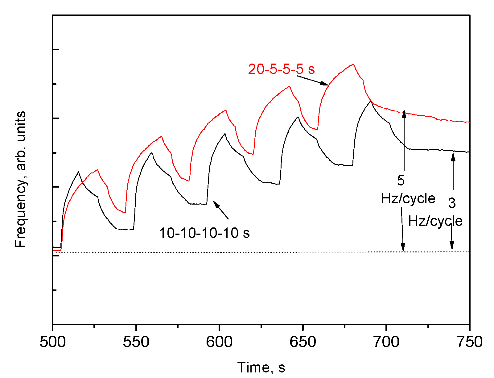
Figure 1.
The illustrative image of quartz crystal monitoring (QCM) frequency change recorded during 5 atomic layer deposition (ALD) cycles with time parameters of 20-5-5-5 s (red line) and 10-10-10-10 s (black line) at 140 °C. Long cycle times were recorded to show the appropriate self-limiting ALD process. At the same time, shorter cycle times, like 2-2-2-5, were sufficient to deposit the films.

Figure 2.
Representative SEM image (left panel, cycle times 2-2-2-5 s at 140 °C) and grazing incidence X-ray diffractometry (GIXRD) patterns (right panel) for the cupric (CuO) films grown on Si substrate by using 500 ALD cycles.
Figure 2.
Representative SEM image (left panel, cycle times 2-2-2-5 s at 140 °C) and grazing incidence X-ray diffractometry (GIXRD) patterns (right panel) for the cupric (CuO) films grown on Si substrate by using 500 ALD cycles.

Figure 3.
Representative X-ray diffraction patterns of CuO thin films grown on SiO2/Si substrate by using different number of deposition cycles indicated by labels.
Figure 3.
Representative X-ray diffraction patterns of CuO thin films grown on SiO2/Si substrate by using different number of deposition cycles indicated by labels.

Figure 4.
Representative SEM images of the 94 nm (5000 cycles, left panel) and 158 nm (10,000 cycles, right panel) thick CuO films.
Figure 4.
Representative SEM images of the 94 nm (5000 cycles, left panel) and 158 nm (10,000 cycles, right panel) thick CuO films.

Figure 5.
Representative SEM images of 3D structures, called stacks, in the left panel, top view of the stack; in the right panel, the CuO film inside 3D substrate (stack) are shown.
Figure 5.
Representative SEM images of 3D structures, called stacks, in the left panel, top view of the stack; in the right panel, the CuO film inside 3D substrate (stack) are shown.

Figure 6.
Electrical resistivity of CuO film grown after 5000 ALD cycles, with the thickness of 94 nm, i.e., with the maximum thickness where the phase was still appropriate [25], measured in zero magnetic field (left panel). The inset shows the low-temperature region (left panel, inset). Electrical resistivity of Si substrate (right panel). The lnρ vs. 1/T plot is shown in the inset, and the red line is a linear fit of the data (right panel, inset).


Table 1.
X-ray reflectivity analysis results of thickness, crystallite size, density, and roughness (with standard deviations) of the CuO films on Si/SiO2 substrate.
Table 1.
X-ray reflectivity analysis results of thickness, crystallite size, density, and roughness (with standard deviations) of the CuO films on Si/SiO2 substrate.
| ALD Cycles | Thickness, nm | Crystallite Size * nm * | Density, g/cm3 | Roughness, nm |
|---|---|---|---|---|
| 500 cycles | 19.5 | 5.6 | 6.1 | 1.2 |
| 2000 cycles | 51 | 8.7 | 6.2 | 2.2 |
| 5000 cycles | 94 | 10.6 | 6.2 | 5.9 |
| 10,000 cycles | 158 | 13.1 | 6.1 | 8.0 |
* GIXRD reflection at 35.6° was used for evaluating the size of crystallites in accord with the Scherrer’s formula and using standard reference material SRM-660 (LaB6) to take into account instrumental broadening, one could obtain X-ray crystallite size varied in different structures in the range of 5.6–13.1 nm (standard deviation ~1 nm).
© 2020 by the authors. Licensee MDPI, Basel, Switzerland. This article is an open access article distributed under the terms and conditions of the Creative Commons Attribution (CC BY) license (http://creativecommons.org/licenses/by/4.0/).
Share and Cite
MDPI and ACS Style
Tamm, A.; Tarre, A.; Verchenko, V.; Seemen, H.; Stern, R. Atomic Layer Deposition of Superconducting CuO Thin Films on Three-Dimensional Substrates. Crystals 2020, 10, 650. https://doi.org/10.3390/cryst10080650
AMA Style
Tamm A, Tarre A, Verchenko V, Seemen H, Stern R. Atomic Layer Deposition of Superconducting CuO Thin Films on Three-Dimensional Substrates. Crystals. 2020; 10(8):650. https://doi.org/10.3390/cryst10080650
Chicago/Turabian StyleTamm, Aile, Aivar Tarre, Valeriy Verchenko, Helina Seemen, and Raivo Stern. 2020. "Atomic Layer Deposition of Superconducting CuO Thin Films on Three-Dimensional Substrates" Crystals 10, no. 8: 650. https://doi.org/10.3390/cryst10080650
Note that from the first issue of 2016, this journal uses article numbers instead of page numbers. See further details here.