
Abstract
A room-temperature two-step cost-effective electrochemical technology is proposed for the preparation of free-standing Au nanomembranes. A thin Au film with the thickness less than 100 nm was deposited by pulsed electroplating on a GaAs substrate in the first step, while electrochemical etching was applied in the second technological step to introduce porosity into the GaAs substrate underneath the Au film. It has been shown that detachment of the film from the substrate occurs at optimized parameters of anodic etching. Scanning electron microscopy imaging of the deposited Au film revealed its nanoparticulate structure generated via the mechanism of hopping electrodeposition, i.e. the film proved to consist of a monolayer of Au nanoparticles with the mean diameter around 20–30 nm. It was found that nanoholes with the diameter controlled by the duration of negative voltage pulses can be introduced into the Au film during electroplating. The purity of the detached Au nanomembranes was demonstrated by the energy dispersive X-ray analysis. The flexibility, nanoparticulate structure along with possibilities to transfer the prepared nanomembranes to various substrates make them promising for new optical, plasmonic and electronic applications.
Export citation and abstract BibTeX RIS

This is an open access article distributed under the terms of the Creative Commons Attribution 4.0 License (CC BY, http://creativecommons.org/licenses/by/4.0/), which permits unrestricted reuse of the work in any medium, provided the original work is properly cited.
Membrane technologies have been widely used for gas separation processes, for example, for the hydrogen separation from hydrotreaters in refineries, oxygen/nitrogen separation, and separation of CO2 from natural gas.1 Particularly, composite polymer membranes became used in large-scale industrial gas separation technologies. The purification of hydrogen via selective permeation through a membrane has been considered to be one of the most promising approaches for the production of high-purity hydrogen, as compared to energy intensive pressure swing adsorption and cryogenic distillation processes.2 Apart from polymeric membranes, inorganic zeolite, rare earth oxide, pure-metal and metal-alloy membranes have been reported to produce rather pure hydrogen from CO2-rich stream.2 Among metallic membranes, palladium membranes have been exploited for both hydrogen production and hydrogen purification.3–5 A number of polymeric, inorganic and ceramic materials was also used to form membranes applied to water and wastewater treatment.6 In spite of the fact that inorganic membranes are more expensive than organic polymeric ones, they offer some advantages such as temperature stability, resistance towards solvents, narrow pore size distribution, and the opportunity for more sterilization options.7
Inorganic membranes have been prepared from materials such as metals (e.g., Pd, Ag, and their alloys, and steel), carbon, silica, zeolite, and various oxides (e.g., Al2O3, TiO2, ZrO2), nitrides, carbides and similar materials, many of which are semiconducting.8 Metal membranes are usually prepared by three methods: chemical vapor deposition, physical sputtering or electroless plating, among which the last one is the most versatile. Porous metal membranes have recently received increasing attention, and significant progress has been achieved in their preparation and characterization, which resulted in their applications in a number of key industries including wastewater treatment, dairy processing, wineries, and biofuel purification.9 In particular, the application of porous metal filters and membranes with special wettability (superhydrophobic–superoleophilic) for oil–water separation has been reviewed recently.10
Apart from these traditional applications, metallic nanomembranes, especially those of noble metals, significantly expanded their areas of applications over the last decade due to their specific catalytic and plasmonic properties. The occurrence of long-range surface plasmons was disclosed as a phenomenon inherent to metal nanomembranes.11 Plasmonic nanomembranes self-assembled from metallic nanocrystals with highly ordered nanoscopic structures allowed one to control their programmable multifunctionality by adjusting the morphology, composition and size of constituent nanoparticles, as well as by engineering packing order of lattice structures, which proved to be of great practical significance for bottom-up built plasmonic devices and circuits.12 Note that the optoelectronic and nanoelectronic applications are also boosted by the dimensional confinement and quantum effects inherent to nanostructures. Particularly, self-supported nanomembranes exhibit electrical and thermal conductivities which are fundamentally different from their bulk counterparts.
Among noble metals, gold outperforms both palladium and platinum as catalysts for many applications.13,14 Gold is also advantageous from the point of view of its plasmonic properties, since the resonance wavelength of nanostructured gold lies in the red and near-infrared spectral range,11,15–17 which is important for optical and fiber-optic applications. A new electron transport regime was found in a gold-nanoparticle-based suspended nanomembrane due to the plasmon-assisted electron transport at the nanoscale, which opened possibilities for future combinations of plasmonics and nanoelectronics.15 Even greater potential for the next generation of plasmonic sensors, color filters and planar nano-lenses has been provided by nanoperforation of gold nanomembranes.16 Large-area free-standing 100 nm thick gold nanomembranes perforated with nanohole arrays have been recently prepared using a template transfer technique with a replication-releasing procedure.17 An extremely narrow plasmonic resonance with a record figure-of-merit of 240 was found to occur in such nanomembranes, which made them usable as high-performance plasmonic refractometric sensors.
Nowadays, different fabrication techniques at the nanoscale are elaborated to obtain artificial nanoporous membranes. It is worth to mention focused ion beam (FIB) milling as one of the most accurate and high-precision techniques.18–20
Over the last two decades, it has been demonstrated that electrochemistry is one of the most accessible and cost-effective approaches for nanostructuring semiconductor materials in a controlled fashion. Combining two methods, namely electrochemical etching and electrochemical deposition, one-dimensional nanostructures such as nanowires, nanotubes and their networks have been successfully fabricated.21–24 Besides, electrochemistry proved to be an indirect tool for the characterization of semiconductor materials. The non-uniformity of doping in bulk GaN grown via Hydride Vapor Phase Epitaxy (HVPE) was disclosed through electrochemical etching,25 while gold electroplating was successfully used for assessing the conductivity of InP nanostructures fabricated by anodic etching of crystalline substrates.26
Electrodeposition provides good accuracy for the control of nanomembrane thickness. However, realization of uniformly-distributed nanoperforation in a membrane is challenging, since nanoperforation is produced by self-organized processes during electrodeposition, which cannot be totally controlled. FIB technologies assure better control of nanoperforation. However, there are some disadvantages in using FIB techniques, such as (i) the nanopores are formed one by one, requiring longer time; (ii) the processed scale is limited by working space of FIB; (iii) the need of expensive equipment makes this method cost-ineffective. Moreover, high energy Ga+1 ions used for milling lead to contamination via ion incorporation, thus the physical and electrical properties can be affected.27
Fabrication of free-standing and large-area nanomebranes is also an important issue, since the free-standing state provides good flexibility of the membrane, which is extremely required, for instance, in the development of wearable physical sensing platforms for healthcare and biomedical applications, including wearable consumer electronics, soft robotics, smart medical prosthetics and electronic skins, etc, in which the metallic nanomembranes would play the role of conductive materials.28–32 In this context, the term of large-area means possibilities to cover some regions of the human body. A serpentine-shaped ultrathin Au membrane was integrated for interconnections in a flexible and stretchable physical sensing platform for physiological monitoring and assessment.33 It was shown that gold thin films with the thickness under 100 nm can withstand uniaxial stretching to 100% strain.31 Flexible electronics proved to be an important component for seamless health monitoring and the development of human-machine interfaces. It was shown that the Au-nanomembrane based systems have the advantages of electrical stimulation and simultaneous sensing, which provides sensorimotor control of a robot arm.34 Resistive pressure sensors have been developed on the basis of freestanding membranes consisting of gold nanoparticles.35
All these platforms are based on effective hetero-integration of components with advanced optical, stretchable mechanical, optomechanical, plasmonic, piezoelectric, triboelectric and electronic properties,32,34–36 gold being an important component.
In this article, we present a two-step cost-effective electrochemical technology for the preparation of free-standing Au nanomembranes, including the ones perforated by nanoholes.
Experimental
Crystalline 500-μm thick Si-doped n-GaAs (100) wafers with the free electron concentration of 1.2 × 1018 cm−3 supplied by MaTeck GmbH, Germany were used as substrates. Prior to electroplating and anodization, the samples were sonicated in acetone for 5 min, cleaned in distilled water and dried. To remove the native oxide from the surface, the samples were dipped in a HCl/H2O solution with the ratio (1:3) for 3 min.
Electroplating of Au was carried out in a commercially available gold bath containing 5 g/l Au (DODUCO). The electrochemical deposition of Au was performed at T = 25 °C in a common two-electrode plating cell where the GaAs wafer served as working electrode, while a platinum wire was used as counterelectrode. A pulsed rectangular shape negative voltage of −16 V was provided by a generator. The metal species were electrochemically reduced on the surface of the sample being in contact with the electrolyte, during the pulse time from 10 μs to 1 ms. A delay time as long as one second was kept after each pulse. Besides, magnetic stirring provided appropriate conditions for the recovery of the ion concentration in the electrolyte. The total time of the electrochemical deposition was 2 min.
For the purposes of comparison, gold films were also deposited by sputtering using a Cressington Sputter Coater 108 Auto instrument under current intensity of 40 mA for 45 s, at the distance of 45 mm between the sample and target, resulting in 50 nm deposited film.
Anodization was performed in potentiostatic regime at room temperature (T = 25 °C) after gold film deposition. The electrical contacts to the sample were prepared with silver paste, then the sample was pressed against an O-ring in a Teflon cell with the 0.2 cm2 area exposed to the 1 M HNO3 electrolyte. The experiments were performed in three-electrode configuration: a Pt mesh with the surface area of 6 cm2 acting as counterelectrode, a saturated Ag/AgCl reference electrode and the sample as working electrode.
The morphology of samples was investigated by using scanning electron microscopes (SEM) Zeiss Sigma and TESCAN Vega TS 5130 MM equipped with an Oxford Instruments INCA Energy EDX system operated at 20 kV for chemical composition analysis.
Experimental Results and Discussion
The proposed method for the preparation of free-standing Au nanomembranes comprised two technological steps. A continuous layer consisting of Au nanoparticles was deposited by pulsed electroplating on a semiconductor (GaAs in our case) wafer in the first step, followed by anodization of the sample in a 1 M HNO3 electrolyte in the second step (see Fig. 1).

Figure 1. (a) Schematic representation of the technological route for the fabrication of Au nanomembrane on a porous semiconductor substrate with possibilities to be transferred to another substrate. Inset is the illustration of the mechanism of hopping electrodeposition of a monolayer of Au nanodots.
Download figure:
Standard image High-resolution imageThe formation of a continuous layer of Au nanoparticles on the surface of the GaAs substrate was previously explained on the basis of mechanism of hopping electrodeposition37 (see the inset in Fig. 1). According to this mechanism, gold dots are nucleated at the beginning of electroplating, followed by their gradual growth in size. As the transverse dimensions of the dot reach a threshold value, a Schottky barrier emerges, the barrier potential being oriented in the opposite direction relative to the applied cathodic voltage. The Mott-Schottky limit was found to be reached at the metal dot diameter of around 20 nm on the surface of n-GaP and n-InP substrates.37,38 It was assumed that the modified local potential "switches off" the electrodeposition within the area of the dot reaching the threshold size. To keep the process running, the system initiates the nucleation of new dots, i. e. the electrodeposition occurs in a hopping mode: Au deposition "jumps" to other local areas as soon as one or more dots reach the threshold value of the diameter. The processes of "switching off" and "hopping" continue until the entire surface exposed to the electrolyte is covered by a monolayer of self-assembled Au nanoparticles. If one compares the Mott-Schottky limit of Au-GaAs interface with that of Au-GaP and Au-InP interfaces, one should mention that the electron affinity of GaAs (4.07 eV) is intermediary between GaP (3.8 eV) and InP (4.38 eV). In this connection the Mott-Schottky limit is expected to be reached at the same Au dot diameter of around 20 nm on the surface of n-GaAs substrates. However, one should take into consideration that the real Schottky barrier height is also affected by the Fermi-level pinning at the metal–semiconductor interface and by the chemical disorder, thus this issue needs a deeper investigation.
A porous GaAs layer was formed underneath the Au film under anodization with the applied voltage of 3 V, the Au film remaining attached to the formed porous GaAs layer. However, anodization at 4 V and higher led to the detachment of the Au film from the porous GaAs substrate with the formation of a free-standing Au nanomembrane. Note that some nanodots could remain on the surface of the porous GaAs substrate.
The applied voltages during anodization were chosen on the basis of the analysis of polarization curves measured at the beginning of anodization of bulk GaAs, as presented in Fig. 2. One can see that anodization of bulk GaAs under an applied polarization of 4 V leads to increased current density. One should note that a porous layer with high degree of porosity or even nanowires are produced under such conditions of anodization, and this observation corroborates the previously published results on anodization of (100) GaAs crystals with free electrons concentration of 2.67–8.63 × 1017 cm−3 in a KOH electrolyte.39 A similar behavior was observed when anodizing a bulk GaAs substrate covered by a nanoparticulate Au film deposited by electroplating, however with significantly decreased current density, especially for a film deposited with short duration of electroplating pulses (see the red line in Fig. 2). These observations can be explained by the formation during electroplating of small voids between the Au nanoparticles constituting the Au film, thus enabling the electrolyte to penetrate through the Au film in the process of anodization and to enter into contact with the surface of the bulk GaAs. Longer pulse duration applied during electroplating led to visible bubble formation at the GaAs surface. Usually, hydrogen or oxygen liberations are the major cause of bubble formation. Generally, bubble formation can affect many electrochemical systems. For example, bubbles formed on the surface of the electrode reduce their effective surface area, causing fluctuations in the current density and affecting the rate of reaction. As a result, the gold is not deposited on sites occupied by these bubbles on the GaAs surface. Note that platting in an ultrasound bath can significantly reduce the impact of bubbles upon deposition. On the other hand, the control of bubbles formation by changing the pulse duration allows one to control the perforation of the produced gold membrane. In order to demonstrate the effect of gold film perforation upon the anodizing of the GaAs substrate, a sample has been prepared with a more compact and continuous gold film deposited by magnetron sputtering. The value of the current in the polarization curve for such a sample proves to be very low (see the green line in Fig. 2), which indicates that no reaction occurs at the semiconductor-electrolyte interface.

Figure 2. Polarization curves measured at the beginning of the anodization process in 1 M HNO3 electrolyte at a scan rate of 50 mV s−1 for (100) bulk GaAs (black line), and bulk GaAs with gold films deposited via pulsed electroplating with pulse duration (width) of 300 μs (blue line) and 50 μs (red line). The green line is measured with a bulk GaAs substrate covered by an Au film deposited by sputtering.
Download figure:
Standard image High-resolution imageFigure 3 shows SEM images of an Au nanomembrane detached from the porous GaAs substrate as a result of anodization at the applied voltage of 4 V. The electroplating of Au was performed under negative voltage applied for 10 μs. The anodization at the applied voltage of 4 V implies a higher current density as compared to anodization at 3 V. The application of higher current density results in the formation of porous GaAs layer with higher degree of porosity, which leads to fewer contact points between the crystalline GaAs surface and the deposited Au layer. At the same time, the higher current density gives rise to more intense electrochemical reactions and the generated gaseous species subject a pressure toward the Au film, thus leading to the detachment of the Au nanomembrane. One can see that the surface of the nanomembrane from the side of the substrate is rather smooth, while the topology of the upper surface reflects individual Au nanoparticles as constituents with the mean diameter around 30 nm. Some traces of Au nanodots are also observed on the surface of the porous GaAs substrate after the detachment of the nanomembrane (Fig. 3c). This is indicative of good adhesion of the Au nanolayer to the GaAs substrate. At the same time, the fabrication of integrous Au nanomembranes with dimensions of several square millimeters is indicative of strong interconnection between the Au nanoparticles forming the nanomembrane, thus ensuring its mechanical robustness. As mentioned above, the nanomembrane exhibits very small pores responsible for the penetration of the HNO3 electrolyte through the Au film during anodization, otherwise the porous GaAs layer would not be formed underneath the Au film.
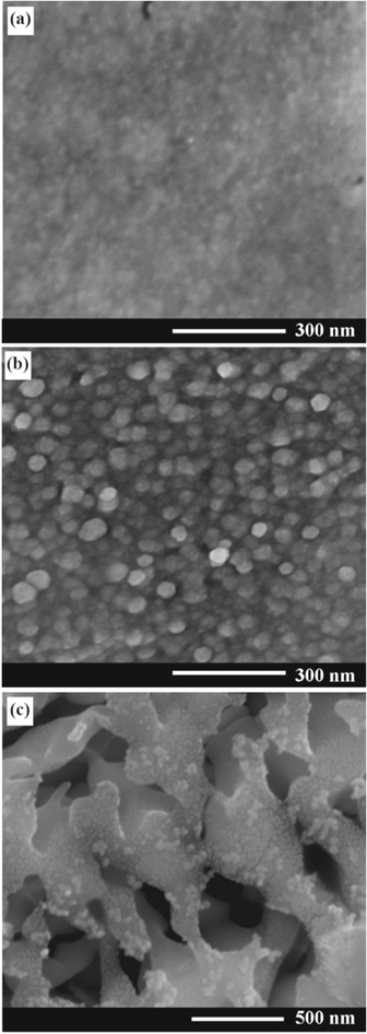
Figure 3. (a) SEM image of an Au nanomembrane detached from the porous GaAs substrate (the side forming the contact with the substrate before detachment). (b) The upper side of the Au nanomembrane. (c) SEM image of the porous GaAs substrate after the detachment of the Au nanomembrane.
Download figure:
Standard image High-resolution imageDue to the robustness of the nanomembrane, it can float in the free-standing state in a liquid (HNO3 electrolyte in our case), or be easily transferred onto another substrate, for instance on a TEM grid for further investigations. Glass, bulk or porous semiconductors can also serve as alternative substrates. In spite of the small thickness of the nanomembrane (less than 100 nm) it can be easily observed by naked eye.
The purity of the prepared Au nanomembranes was demonstrated by the energy dispersive X-ray analysis of two nanomembranes: one on the porous GaAs substrate (Fig. 4) and another one after being transferred to a Cu TEM grid (Fig. 5). No other elements were found except for the Au in the nanomembranes and the elements present in the GaAs substrate or in the TEM grid. According to the performed investigations, the content of Au over the surface of the membrane varies from 18 to 19 atomic % in Fig. 4, and from 13 to 14 atomic % in Fig. 5, which is in limits of the errors defined by the instrumental accuracy. These observations are indicative of the uniformity of the Au film thickness over the entire Au nanomembrane. Figure 5 demonstrates also the transferability of the Au nanomembrane.
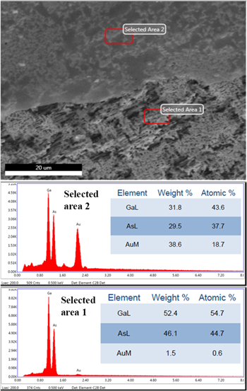
Figure 4. EDX analysis of an Au film attached to the surface of the porous GaAs substrate.
Download figure:
Standard image High-resolution image
Figure 5. EDX analysis of an Au nanomembrane transferred to a TEM grid.
Download figure:
Standard image High-resolution imageThe prepared Au nanomembranes prove to be highly flexible as demonstrated in Fig. 6, where the membrane is not destroyed by a five-times folding. Based on this finding one can conclude that the produced gold nanomembranes are promising for applications in flexible electronic devices.

Figure 6. (a) An overall SEM view of a folded Au nanomembrane on the porous GaAs substrate. (b) A magnified secondary electron SEM image. (c) Back-scattered electron SEM image demonstrating the charging effect.
Download figure:
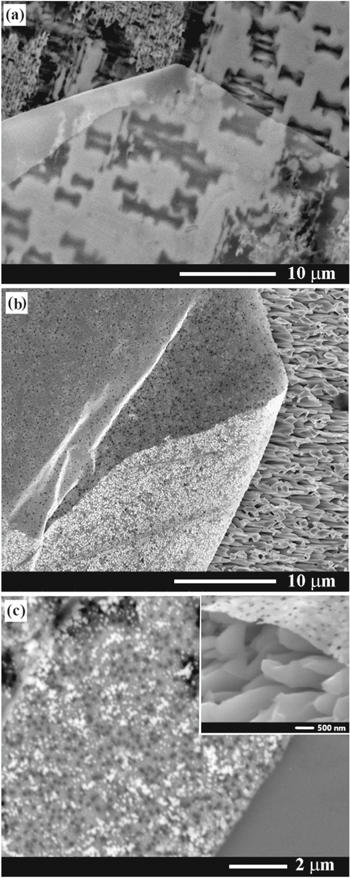
Standard image High-resolution imageAnother important issue is related to the possibilities to control the degree of porosity of free-standing membranes. As mentioned above, the Au nanomembrane prepared by electroplating with pulse duration of 10 μs contained very small pores, even not observable in Fig. 3. By increasing the pulse duration to 300 μs, a porous Au membranes have been obtained with the mean diameter of pores around 100 nm, as shown in Figs. 7b, 7c.
Figure 7. (a) SEM image of an Au nanomembrane prepared by electroplating with pulse duration of 10 μs. (b) SEM image of an Au nanomembrane prepared by electroplating with pulse duration of 300 μs. (c) Magnified SEM image of the nanomembrane prepared by electroplating with pulse duration of 300 μs demonstrating the formation of pores with a mean diameter around 100 nm. Inset in (c) is the SEM image of a tilted gold nanomembrane on a porous GaAs layer.
Download figure:
Standard image High-resolution image
The formation of pores is explained by the emergence of gas bubbles on the surface of the GaAs substrate as a result of electrochemical reactions during electroplating. Note that the formation of bubbles was observed by the naked eye when the duration of electroplating pulses was increased to 1 ms. At the same time, the transverse dimensions of pores in the Au nanomembrane increased considerably, and the membrane became less robust.
We established that gold nanomembranes of different shapes can be realized by employing photolithography before the procedure of electrochemical etching. In particular, Au nanobelts with the width of several tens of micrometers, and the length of several millimeters have been prepared based on Au nanomembranes with the thickness less than 100 nm. The thickness of a gold membrane electroplated with the pulse duration of 300 μs was estimated to be around 70 nm from the SEM image inset in Fig. 7c.
Conclusions
The results of this study demonstrated the effectiveness of a two-step cost-effective electrochemical technology for the preparation of free-standing Au nanomembranes. The deposition of a thin (less than 100 nm) nanogranulated Au film on a GaAs substrate during the first step of electroplating proved to be governed by the phenomenon of hopping electrodeposition, which resulted in the formation of a monolayer of Au nanoparticles with the mean diameter around 20–30 nm. By changing duration of negative voltage pulses during electroplating, we succeeded to introduce nanoholes into the Au film with the diameter controlled in the range from tens to hundreds of nanometers. The nanoporous nature of the Au nanofilm ensured its permeability to the electrolyte during the second step of the technological route consisting of anodic porosification of the underneath substrate. Free-standing Au nanomembranes were successfully fabricated by detaching the Au nanofilm from the porous GaAs layer upon increasing the anodization voltage above a threshold value equaling around 4 V in the case of electrochemical etching of GaAs substrates with the free electron concentration of 2 × 1018 cm−3 in a 1 M HNO3 electrolyte. The possibility to transfer the prepared nanomembranes to various substrates was demonstrated, thus making them promising for potential hetero-integration with advanced optical, plasmonic and electronic systems.
Funding
This research was funded by Ministry of Education, Culture and Research of Moldova under the project no. #20.80009.5007.20 and European Commission under the grant no. #810652 "NanoMedTwin".
Acknowledgments
The authors thanks to Dr. Oana Tutunaru for assistance in measurements. Eduard Monaico thanks to the Alexander von Humboldt Foundation for support.
CRediT Authorship Contribution Statement
Eduard Monaico: supervision, Conceptualization, Methodology, Data curation. Elena Monaico: sample preparation, Anodization, Electroplating. Veaceslav Ursaki: validation, Writing—Original draft preparation. Ion Tiginyanu: scientific guidance, Writing and reviewing, Project administration. The manuscript was written through contributions from all authors. All authors have given approval to the final version of the manuscript.