Article

Investigation of Barrier Inhomogeneities and Electronic Transport on Al-Foil/p-Type-4H-SiC Schottky Barrier Diodes Using Diffusion Welding

Thomas Johann Seebeck Department of Electronics, Tallinn University of Technology, Ehitajate tee 5, 12616 Tallinn, Estonia
*
Author to whom correspondence should be addressed.
Crystals 2020, 10(8), 636; https://doi.org/10.3390/cryst10080636
Submission received: 30 May 2020 / Revised: 14 July 2020 / Accepted: 20 July 2020 / Published: 23 July 2020
(This article belongs to the Special Issue Development and Investigation of SiC and SiC-based devices)

Abstract

:
The diffusion welding (DW) is a comprehensive mechanism that can be extensively used to develop silicon carbide (SiC) Schottky rectifiers as a cheaper alternative to existing mainstream contact forming technologies. In this work, the Schottky barrier diode (SBD) fabricated by depositing Al-Foil on the p-type 4H-SiC substrate with a novel technology; DW. The electrical properties of physically fabricated Al-Foil/4H-SiC SBD have been investigated. The current-voltage (I-V) and capacitance-voltage (C-V) characteristics based on the thermionic emission model in the temperature range (300 K–450 K) are investigated. It has been found that the ideality factor and barrier heights of identically manufactured Al-Foil/p-type-4H-SiC SBDs showing distinct deviation in their electrical characteristics. An improvement in the ideality factor of Al-Foil/p-type-4H-SiC SBD has been noticed with an increase in temperature. An increase in barrier height in fabricated SBD is also observed with an increase in temperature. We also found that these increases in barrier height, improve ideality factors and abnormalities in their electrical characteristics are due to structural defects initiation, discrete energy level formation, interfacial native oxide layer formation, inhomogenous doping profile distribution and tunneling current formation at the SiC sufaces.

1. Introduction

During the last few decades, SiC (a wide bandgap semiconductor material) has gained significant importance in a wide range of power electronics applications. SiC exists in many different crystalline forms, which are called polytypes. Among these polytypes, 4H-SiC, 6H-SiC and 3C-SiC are attractive for the development of power electronics devices thanks to their distinct physical and electrical attributes. Meanwhile, 4H-SiC is a potential candidate for high-power device applications due to its low-loss, low series resistance, stability at high-temperature, high electron velocity and its extraordinary high thermal conductivity and high physical and chemical stability, high breakdown voltage properties [1,2,3,4]. As a result of these properties, 4H-SiC-based power Schottky barrier diodes and modules are already commercially available. Temperature dependency for n-type SiC-based devices has been investigated by many researchers [5,6,7] to commercialize the expected applications. However, the prevalence of SiC has not yet been comprehensively exploited in different polytypes. In particular, the promising properties of p-type 4H-SiC have not yet been accomplished to their full potential for use in the fabrication of highly efficient power devices depending on the quality of the SiC layers and metal–SiC contacts. The contact formation process for soldering and attaching dies, (e.g., micro or nanoparticle pastes or solders) and their thermal stability as Schottky contacts have been studied to realize their operational requirements and to improve the performance of SiC-based devices [8,9,10,11]. Direct bonding (DB) technology has significant attention in the development of power electronics and micro electromechanical systems [12]. This DB technology have been used in the metal-film and substrate of the same material or metal-film and substrate of different materials without concern of the crystalline relationship between them. The main concern in DB technology is smoothness of the surfaces without metallic contamination and suitability of bonding surface orientation to achieve defect-free stronger bonding and structures [13]. However, DW (high temperature DB technique) is a solid-state material joining process that can be utilized to bond various contact materials with the high performance semiconductor substrate. The DW technology can help to improve the quality of contacts. It also introduces a technological approach for the realization of the contacts with a thickness over a millimeter (mm). Thick Aluminum (Al) Foil on p-type 4H-SiC forms a contact using DW, which improves the the ability to handle large electric power and also increases the semiconductor device’s current rating [14,15]. Additionally, interface states with high densities are likely to be formed in the DW process. These interface states (caused by pinning of fermi-level) modify the potential barriers at the interface of the diodes [16]. To date, Schottky barrier height (SBH) investigations have been done by many researchers [17,18] to improve the performance and reliable SBDs on p-type 4H-SiC.
In this paper, p-type-4H-SiC SBDs with Al-Foil as a metal contact have been fabricated for the very first time with a novel technique: DW. A schematic of fabricated diode structures, doping concentration and physically fabricated DW SBD is shown in Figure 1a,b. An attempt has been made here, to deal with distinct aspects of temperature dependent current-voltage (I-V) and capacitance-voltage (C-V), barrier height formation at the metal contact and SiC interface, ideality factor, doping concentration, current transport mechanism, and activation energy plot analysis for Al-Foil/p-type 4H-SiC SBD. The main goal of this work is to explain the inhomogeneity barrier height formations, current transport phenomena, and to observe their influence in identically manufactured (with the same vacuum pressure, contact force and annealing temperature) Al-Foil/p-type 4H-SiC SBDs using experimental I-V-T and C-V-T characteristics.

2. Sample Preparation and Experimental Procedure

This section contains the experimental details and procedures that have been adopted to develop p-type 4H-SiC SBD.

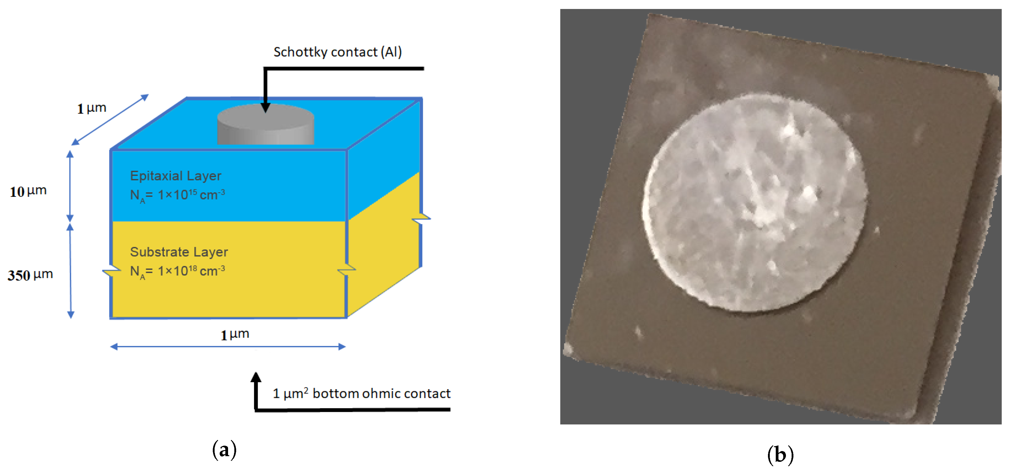
2.1. Sample Preparation Procedure

The SiC wafers that were used for this SBD study were purchased from Cree, Inc., (Durham, NC, USA). These SiC wafers were p-type Al doped with a diameter of 76 mm. The average resistivity of 4.85 Ω -cm, 350 μ m thick wafers were Al doped substrate to a concentration of 1 × 10 18 cm 3 , followed by 10 μ m thick p-type epitaxial layers doped to a concentration of 1 × 10 15 cm 3 . Si-face 4H–SiC (0001) 4 off-axis surface orientation has been polished by the chemical mechanical method on the bonding face of the wafer (i.e., the side to which diffusion bond will be made). All of the wafers were diced into 10 × 10 mm 2 samples.
In the next step, surface preparation and cleaning has been done in three sequential steps. First, each sample was cleaned with a dredge in methanol for 5 min. Then, the sample was dipped in a solution of (48%) diluted HF, consisting of H 2 O:HF (25:1) for 5 min to remove any native oxide (SiO 2 ) on the front and backside of the surface epi-layer and substrate layer, respectively. In the next step, the samples were dredged by rinsing in normal water for 5 min. Finally, each sample was cleaned in deionized (DI) water, at room temperature for 5 min.
Furthermore, the DW process has been used to deposit the Al-Foil as a metal contact with a diffusion pumped chamber at a base pressure of not less than 1 × 10 4 mbar. The Al-Foil and SiC surface were brought into contact with each other under a pressure of 750 N force ( for 5 min) at 575 C temperature for 15 min. Finally, at the same time, 100 μ m thick of Al-Foil was welded as an ohmic contact on the entire surface backside of the SiC substrates and 60 μ m thick of Al-Foil was welded as a Schottky contact on the center of the SiC epitaxial layer.

2.2. Electrical Measurement Procedure

The electrical properties at the interface of Al-Foil and p-type 4H-SiC depend on several factors such as treatment on surfaces of the substrate before bonding, temperature, contact force, subsequent annealing while DW bonding. It is noteworthy that prior to bonding, no RCA cleaning procedure was introduced on the surface of the 4H-SiC sample. The cleaning procedure was done in a normal environment. In this article, our motivation was to observed and represent Al-Foil/p-4H–SiC electrical behavior and inhomogeneities within identically manufactured Schottky barrier diodes. We have manufactured nine diodes by diffusion welding (DW) technology. These nine diodes are manufactured with identical cleaning process and same manufacturing process parameters. Here, we emphasized the comparative study of barrier inhomogeneities and current handling capabilities of these identically manufactured Schottky diodes. So, we have chosen two diodes out of nine SBDs. The I-V and C-V characteristics on these two p-type 4H-SiC SBD (DWS#III and DWS#IX) with the thickness of 365 ( ± 2 ) μ m measurements were performed in a temperature range of 300 K–450 K. These SiC Schottky diodes are placed in an enclosed probe station integrated with a DLS-83D temperature controller from Semilab Co. Ltd. The comparative study also observed another seven Al-Foil/p-type 4H-SiC SBDs that were identically manufactured by DW techniques, having an average thickness of 365 (±2) μ m. However, the temperature dependence of I-V characteristics of the DWS# III and DWS# IX was also measured at high temperature with a Keithley 2400 source and measurement unit, with a dedicated LabVIEW program current that was set up to 1A.

3. Results and Discussion

This section is divided into four subsections: temperature dependent I-V, C-V characteristics, discussion of the I-V, C-V results, and the activation energy plot are discussed based on the electronic transport and barrier inhomogeneities for p-type 4H-SiC based Al-Foil contact SBDs.

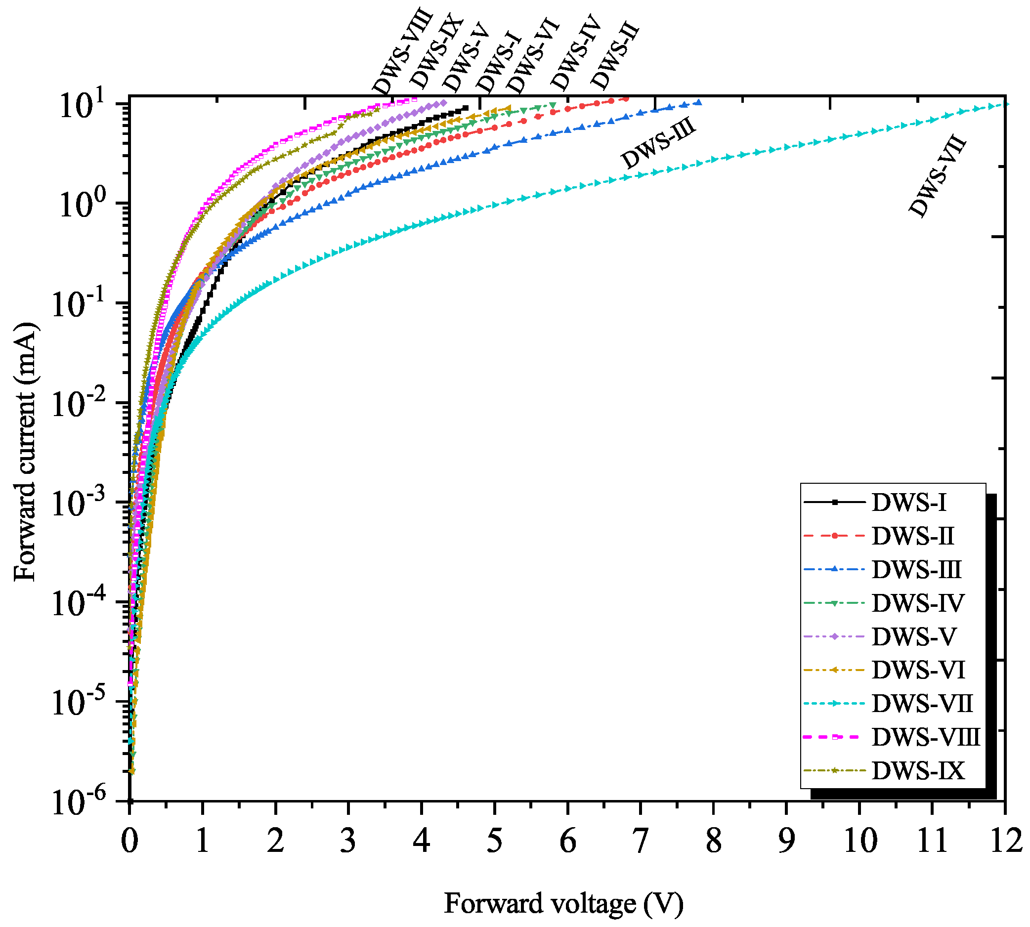
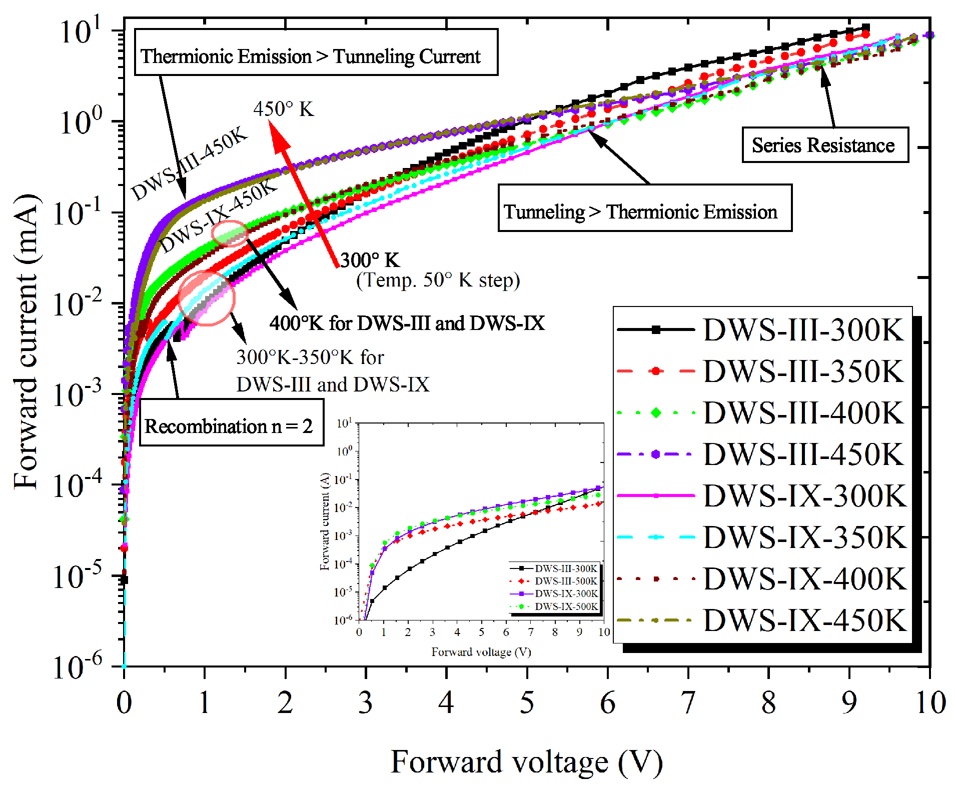
3.1. Temperature Dependence of I-V Characteristics

Al has been extensively used as a metal contact and interconnects in semiconductor devices, especially for Schottky contacts because it has a low SBH and low resistivity which results in a lower forward voltage drop. However, the barrier height is of concern for current carrier transport mechanisms through the metal and 4H-SiC barrier interfaces. Therefore, to accomplish a complete understanding of the current transport across the diffusion welded Al-Foil/p-4H–SiC contact SBD characteristics, it is necessary to take into the consideration of thermionic emission (TE) [19], interface state density distribution [20], the image-force lowering [21], the recombination and quantum-mechanical tunneling [22,23], distinctive high level of TFE [24] and also the lateral distribution of BH inhomogeneities [25,26] that influence the device current capabilities [27,28]. The DLS-83D measurement unit exhibits a forward I-V characteristic, as shown in Figure 2. This figure shows the rectifying properties of nine (DWS#I-IX) Al-Foil/p-type 4H–SiC SBDs at room temperature.
Additionally, two diffusion welded diodes (DWS# III and DWS# IX) are utilized for temperature-dependent I-V characteristics out of nine SBDs to study the barrier inhomogeneties and current transport process. The Figure 3 show exponential behavior over a voltage range in forward I-V-T characteristics for the SBDs DWS# III and DWS# IX at temperatures 300 K–450 K.
The forward current dramatically increases with temperature, as shown in Figure 3. This represents the various mechanisms of current transport dependence on temperature. It can also be observed that the measurement of forward current bulges more at high temperatures, while the thermionic emission current mechanism encountered overloads the tunneling current. However, this bulge is reduced by increasing the applied forward voltage, where the tunneling current is more prominent over the thermionic emission current, as shown in Figure 3 for the diffusion welded DWS# III and DWS# IX diodes with a temperature step of 50 K. Furthermore, a keithley 2400 and 4-point measurement unit (current set up to 1A) measures the temperature dependent forward I-V characteristics for the p-type 4H-SiC-SBD (DWS# III and DWS# IX) at room and 500 K, as shown in the inserted Figure 3. In particular, inserted Figure 3 clearly shows that with identically manufactured devices have different current loading mechanisms at different temperatures. This variation in the current handling capabilities of identically manufactured devices may be due to the thermal annealing process integrated during DW technology, as well as the cleaning process before fabrication. The total forward current that is affected by each of these temperatures at forward bias voltage for current-carrying an ideal homogeneous SBD (without considering small series resistance) can be better described by thermionic emission theory [28],
I = I s exp q V n K T 1 exp q V K T
I s = A A T 2 exp q Φ B 0 K T
where, I is the total forward current, I s is the saturation current, Φ B 0 is the BH, A is the area of the diode, n is the ideality factor, and A* is effective Richardson’s constant (146 Acm 2 K 2 ), k is the Boltzmann’s constant, q is the electron charge and T is the absolute temperature [29,30,31]. The temperature-dependent Φ B 0 , n and I s can be extracted from the experimentally obtained forward (I-V) characteristics, which will clarify the conduction mechanism in the Al-Foil/4H–SiC SBDs.
For this purpose, the Chung and Chung procedure [32] is used to extract these parameters from the I-V characteristics. The saturation current I s and the ideality factor (n) can be determined from the intercept of experimental ln (I) versus voltage (V) plot at zero voltage and the slope of the linear forward region of the ln (I) versus V plot respectively. Once I s is determined, the barrier height Φ B 0 and ideality factor n can be evaluated from following equations (Equations (3) and (4)) by rearranging Equations (1) and (2):
Φ B 0 = K T q l n A A T 2 I s
n = q K T V ( l n I s )
Figure 4 shows the apparent barrier height and ideality factor extracted from the p-type 4H-SiC-SBD (DWS# III and DWS# IX) with temperature range 300 K–450 K dependent I-V characteristics. These obtained BH and ideality factor characteristics help to understand the behavior of the inhomogeneous potential barrier. Figure 4 demonstrate that the ideality factor decreases with increasing temperature, whereas Schottky BH increases with the increasing temperature. The large value of the ideality factor, particularly at room temperature, for both of the identically manufactured SBDs are shown in Figure 4. In DWS# III SBD, it is noted that the value of SBH Φ B 0 has ranged from 1.03 eV to 1.42 eV, and the ideality factor decreases from 1.98 to 1.34 with increasing temperature. Barrier height variation is observed in two identically manufactured SBDs, where BH of DWS# III slightly higher than that of DWS# IX SBD are shown in Figure 4.
Unlike the DWS# III, DWS# IX SBD shows that the value of SBH ( Φ B 0 ) has ranged from 0.95 eV to 1.35 eV and the ideality factor decreases from about 2.45 to 1.95 with increasing temperature. However, Raghunathan et al. [33] and other researchers [34,35] obtain a high value of the ideality factor and low value of the barrier height at low or room temperature.
These dissimilarities within identically manufactured SBD devices suggest that the recombination current is dominated at low forward voltage regions instead of classic thermionic emission theory, which is also shown in Figure 3. The noted barrier height and ideality factors divergent in both identical SBDs is resulted due to the lower electron mobility of p-type 4H-SiC-SBD in fractional ionization of impurities and the structural defects that are initiated by surface preparation processes or during the deposition process additionally contribute as a carrier recombination center at room temperature [36].

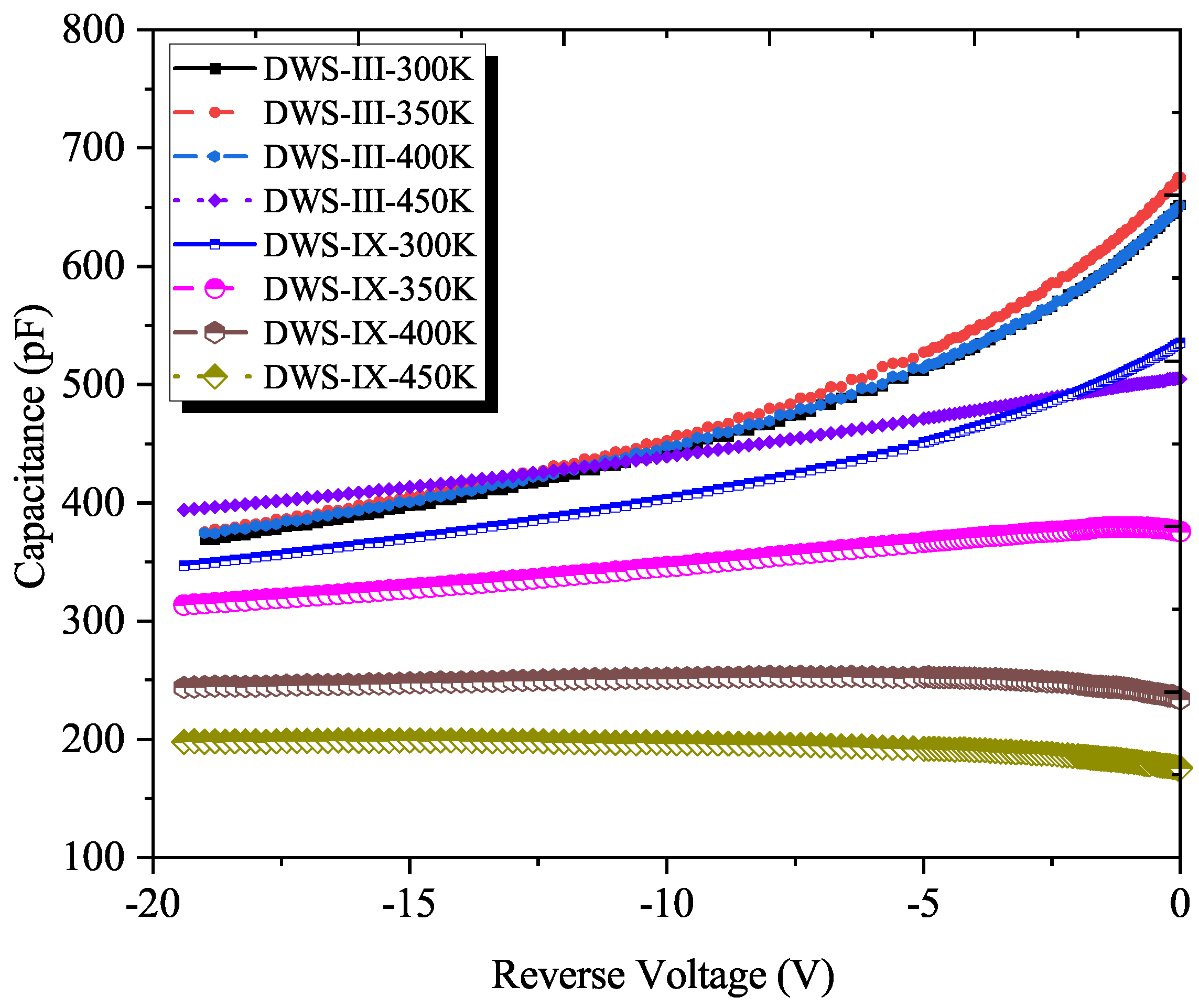
3.2. Temperature Dependence of C-V Characteristics

In the first scenario, the capacitance-voltage (C-V) characteristics of nine p-type identically manufactured SBDs are measured as shown in Figure 5. Except for some anomalous nature, all of the DW manufactured SBDs (DWS# I-IX) show typical C-V characteristics. Additionally, temperature dependent C-V characteristics were measured on DWS# III and DWS# IX SBDs for the SBH to study their atypical nature with a temperature range from 300 K–450 K, as shown in Figure 6. Unlike DWS# III SBD, DWS# IX shows distinct C-V-T characteristics, where a decrease in capacitance with increasing temperature is observed, as shown in Figure 6. In Figure 6 the C-V-T characteristics also shows abnormality at a higher temperature (450 K) for both DWS# III and DWS# IX SBDs. However, here it is noted that the DWS# III SBD represents more than double capacitance value at room temperature compared to that of DWS# IX at 450 K. This distinct nature within an identically manufactured SBDs could be due the to homogenous doping profile distribution. For a semiconductor with a homogenous doping profile, the differential capacitance C = d Q d V can be expressed by:
C = C 0 V b i V r
where
C 0 = A ε q N D 2 ; ε = ε 0 ε r e l
In our previous paper [16], it was observed that capacitance increases with the temperature increases, such as the normal C-V-T characteristics for n-type 4H-SiC SBDs. However, for the DWS# III and DWS# IX SBDs, the discrepancy between these C-V-T characteristics can be explained by assuming the presence of inhomogeneous barrier height and the device processing as well as the measurement environment conditions, which will be discussed in the following sections.
The BH and doping concentration can be determined from the voltage intercept in plotting 1/C 2 as a function of reverse voltage using the standard equation [36]:
1 C 2 = 2 q ε s ε 0 N D A 2 ( V b i V r )
Φ B 0 = V b i + V n
V b i = V i + K T q
V n = K T q l n ( N C N D )
Φ B 0 = V i + K T q 1 + l n ( N C N D )
where N D denotes the doping concentration, V i is the diffusion potential (voltage intercept), V b i is the built-in voltage, V r is the reverse voltage, V n is the depth of the Fermi level (between the Fermi level position and conduction band edge), N C is the effective density of states in the conduction band, ε s is the static dielectric constant and ε 0 is the permittivity of free space and kT is the thermal energy. But at zero reverse voltage; the capacitance depends on doping density ( N D ) and building voltage without considering the effect of image force can be represented as:
V b i = Φ B 0 E C E F n K T q
These diode doping concentrations and built-in voltages were obtained by rearranging Equation (6) from the slope and intercept of 1/C 2 vs. V r plot. The value of the barrier height is then determined from Equation (10). At the same time, the build-in voltages of the DW SBDs are obtained by extrapolating intersection of 1/C 2 vs. V r axis, which can be express by Equation (6).
Figure 7 shows the BH and doping concentration analysis obtained from the measurement of C-V-T values that justified the C-V-T characteristics. Here, it is remarkable that the higher inhomogeneous doping profile is present in DWS# IX SBD and it is one order magnitude higher than DWS# III. Additionally, the DWS# IX barrier height is lower compared to that of DWS# III SBD. Nonetheless, the values of the extracted SBH by means of C-V technique increase significantly as the temperature increases, as shown in Figure 7. The investigated SBH and doping density are evidently related to the effect of lattice defects in the silicon carbide, by a non-uniform interface creating inhomogeneity in the BH or thin oxide film introduced in the interface region (between Al Foil and silicon carbide layer), that was reported by Lundberg et al. [37]. Consequently, the barrier capacitance influenced in the identically manufactured DW Al-Foil/SiC Schottky contact is due to the decrease in the barrier height and formation of unknown existence of an intermediate layer.

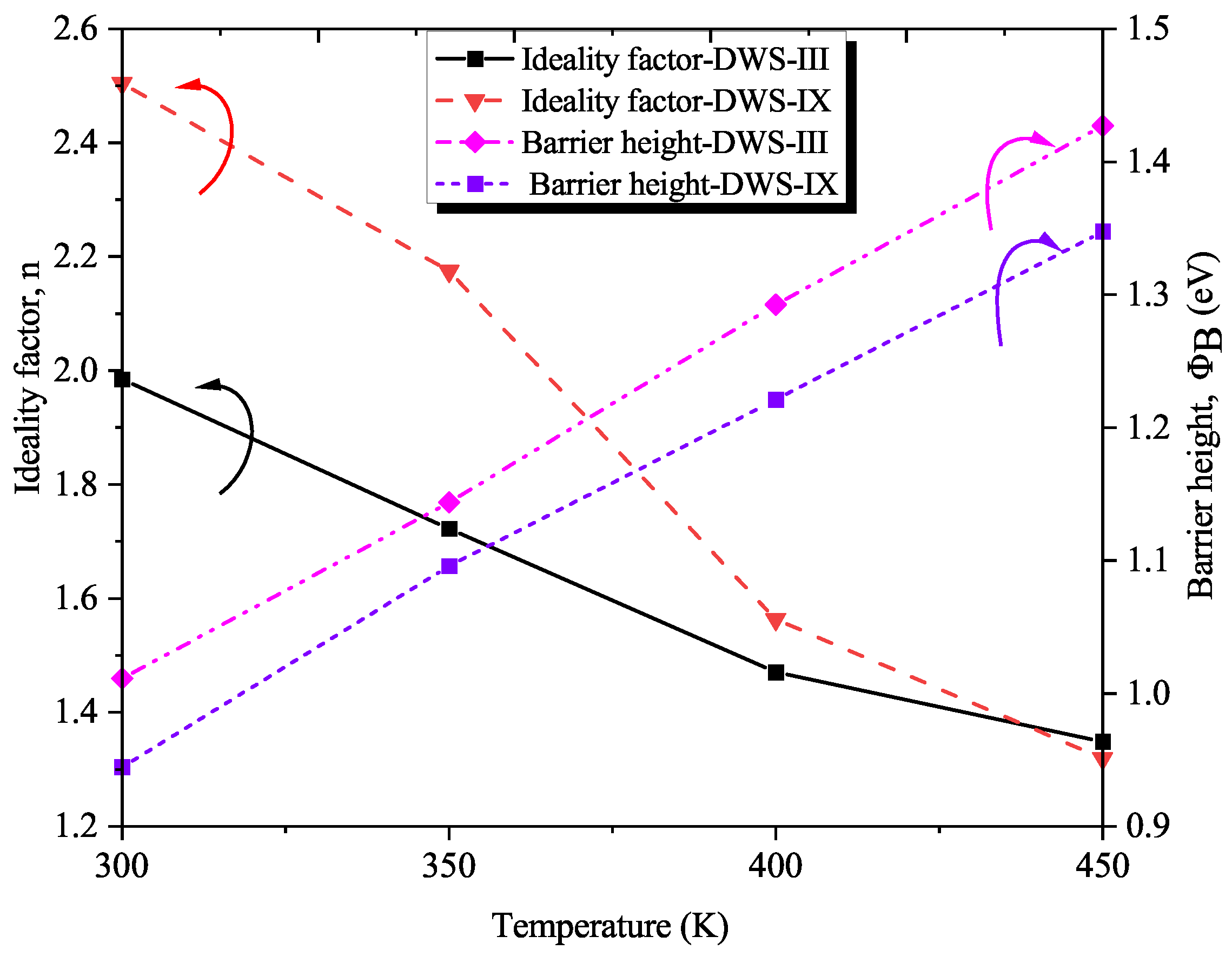
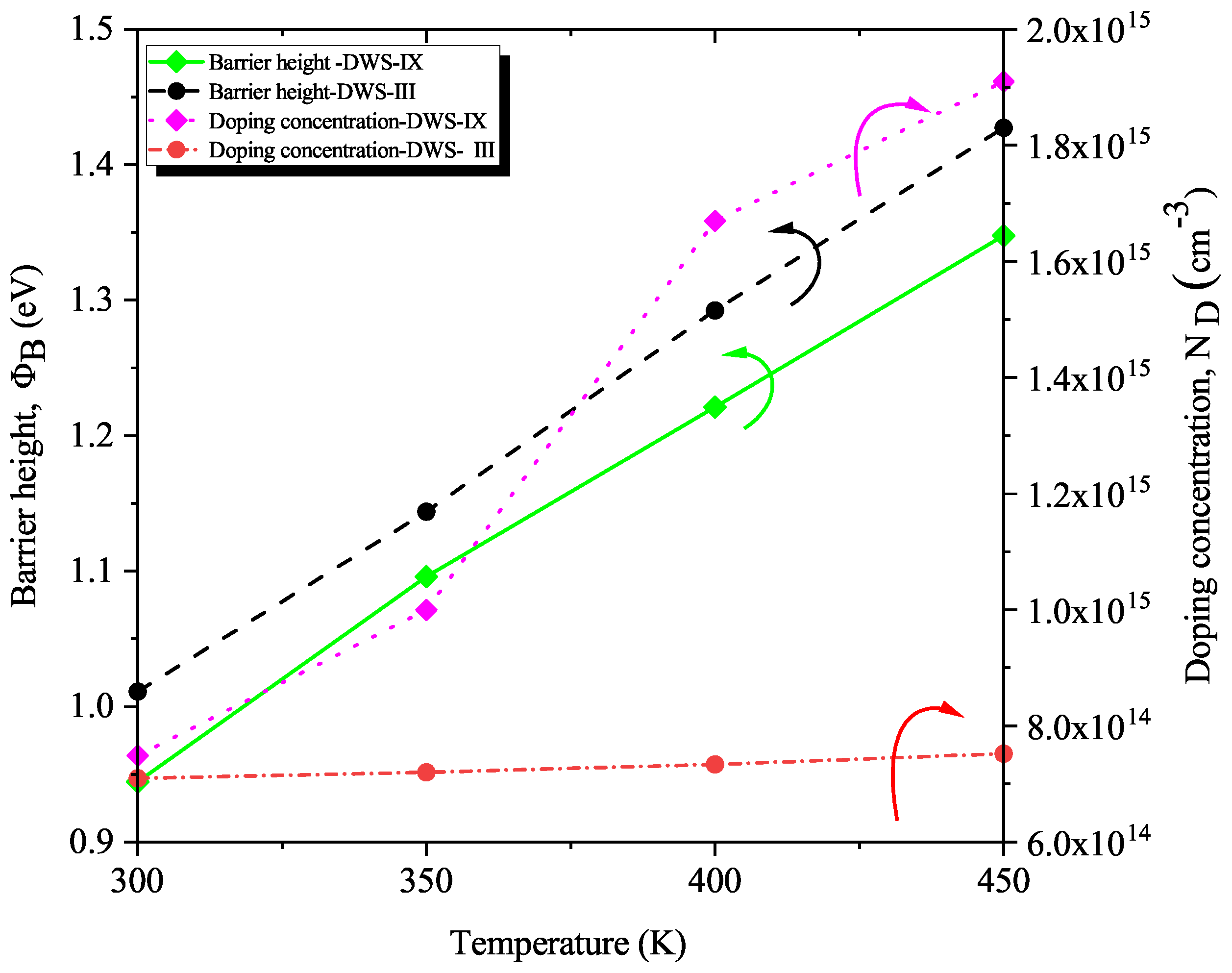
3.3. Discussion of the I-V-T and C-V-T Results

The barrier heights of DWS# III and DWS# IX SBDs fluctuate about 0.04 eV and 0.07 eV for the I-V-T and C-V-T measurements, respectively, as noted in Figure 4 and Figure 7. Here, we can observe that the BH variation is not significantly affected in C-V-T compared to that of I-V-T characteristics. The BH resulting from the I-V-T and C-V-T characteristic values illustrate that barrier inhomogeneity strongly depends on in the interface layer, which is caused by a slightly induced BH lowering. Another cause of the higher dependency of BH on C-V-T characteristics can be explained by the locally induced non-uniform interfacing lateral BH, which approaches the flat-band SBH [38,39].
Furthermore, the barrier heights obtained from C-V-T characteristics are not mainly dependent on the ideality factor and therefore they are more compatible for the individual diode, as shown in Figure 7. These interfacing lateral BHs can be associated with the particular conditions, such as the cleaning preparation of these SBDs and the fabrication processing steps, especially annealing temperature [40]. This reduction in the barrier height is one of the main reasons for the effect of an intermediate layer between Al-Foil and 4H-SiC semiconductor epi-layer. Another possible justification is that a thin oxide layer is created at the interface during sample preparation, which can also act as additional capacitance in C-V measurements. Consequently, we can conclude that current through the contact may be significantly influenced by the existence of the inhomogeneity of BH’s and this can be more justified by considering the activation energy plot for both identical Schottky diodes.

3.4. Activation Energy Plot Analysis

The activation energy plot of ln ( I s / T 2 ) versus 10 3 /T expression can be retrieved from Equation (2)
l n ( I s T 2 ) = l n ( A A ) ( q K T ) Φ B 0
The values of activation energy plot were calculated from the normalized I-V-T DWS# III and DWS# IX of Al-Foil/p-type 4H–SiC SBDs as shown in Figure 8. Here, the term ln ( I s / T 2 ) dealings with two almost parallel regions for both (DWS# III and DWS# IX) SBDs are independent of applied potential. These lines within two parallel non-uniform regions are anomalous due to the inhomogeneous barrier or potential fluctuations between the Al-Foil and p-type SiC epi-layer interface layer. Therefore, from these discussions, and taking into account the formation of the activation energy plot, it is assumed that at least two discrete barrier heights are present in each of the SBDs. These barrier heights are mainly concentrated locally as an interface layer existing as regions with relatively lower or higher barrier heights that is developed are due to the temperature at the boundary between these two-barrier heights regions during the formation each of the SBDs.

4. Conclusions

In this work, we fabricated 60 μm-thick-Al foil/p-type-4H-SiC SBDs by DW technology. We observed Schottky like characteristics in all nine manufactured devices with identical process parameters. This investigation found undesired anomalous in their electrical characteristics and observed barrier inhomogeneties present in all SBDs. The SBH and ideality factors are different while comparing within SBDs despite their identical manufacturing process. We also found that the ideality factors is improved by annealing. It observed that at a higher temperature and higher forward voltage, the tunneling current is dominated compared to thermionic emission current mechanism. However, at room temperature, the Schottky junction current influenced by the carrier recombination center is due to incomplete ionization. These results is explained by considering the inhomogeneous barrier height due to discrete energy levels, tunneling current formation, interfacial native oxide layer formation during surface preparation and inhomogenous doping profile distribution. The results suggested that diffusion welded processing parameters and surface preparation steps need to be optimized.

Author Contributions

M.H.Z. and A.K. conceived the idea and M.H.Z. performed the developments of diodes and their experimental works. M.H.Z. drafted the article. T.R.; M.H.R. and A.K. reviewed the article. A.K. and T.R. managed funding of the project. All authors have read and agreed to the published version of the manuscript.

Funding

The Estonian Research Council through the projects IUT19-11, PUT1435 and PRG620 supported this research. We thank the support of Horizon 2020 ERA-chair Grant “Cognitive Electronics COEL”—H2020-WIDESPREAD-2014-2 (Agreement 668995; TTU VFP15051) as well.

Acknowledgments

The author would like to acknowledge Oleg Korolkov and Natalja Sleptšuk for their help during measurement related setup and discussion.

Conflicts of Interest

The authors declare no conflict of interest.

References

  1. Lebedev, A.A. Heterojunctions and superlattices based on silicon carbide Semicond. Sci. Technol. 2006, 21, R17. [Google Scholar] [CrossRef]
  2. Kimoto, T. Material science and device physics in SiC technology for high-voltage power devices. Jpn. J. Appl. Phys. 2015, 54, 040103. [Google Scholar] [CrossRef]
  3. Casady, J.B.; Johnson, R.W. Status of silicon carbide (SiC) as a wide-bandgap semiconductor for high-temperature applications: A review. Solid-State Electron. 1996, 39, 1409–1422. [Google Scholar] [CrossRef]
  4. Bakowski, M.; Gustafsson, U.; Lindefelt, U. Simulation of SiC High Power Devices. Phys. Status Solidi A 1997, 162, 421. [Google Scholar] [CrossRef]
  5. Schaffer, W.J.; Negley, G.H.; Irvine, K.G.; Palmour, J.W. Conductivity Anisotropy in Epitaxial 6H and 4H Sic. Mater. Res. Soc. Symp. Proc. 1994, 339, 595. [Google Scholar] [CrossRef]
  6. Pernot, J.; Contreras, S.; Camassel, J.; Robert, J.L.; Zawadzki, W.; Neyret, E.; Cioccio, L.D. Free electron density and mobility in high-quality 4H–SiC. Appl. Phys. Lett. 2000, 77, 4359. [Google Scholar] [CrossRef]
  7. Matsunami, H.; Kimoto, T. Step-controlled epitaxial growth of SiC: High quality homoepitaxy. Mater. Sci. Eng. 1997, 20, 125. [Google Scholar] [CrossRef]
  8. Liu, X.; Liu, W.; Wang, C.; Zheng, Z.; Kong, L. Preparation and Sintering Properties of Ag27Cu2Sn Nano paste as Die Attach Material. J. Electr. Mater. 2016, 45, 5436–5442. [Google Scholar] [CrossRef]
  9. Kim, D.; Chen, C.; Pei, C.; Zhang, Z.; Nagao, S.; Suetake, A.; Sugahara, T.; Suganuma, K. Thermal shock reliability of a GaN die-attach module on DBA substrate with Ti/Ag metallization by using micron/submicron Ag sinter paste. Jpn. J. Appl. Phys. 2019, 58. [Google Scholar] [CrossRef] [Green Version]
  10. Drevin-Bazin, A.; Lacroix, F.; Barbot, J. SiC Die Attach for High-Temperature Applications. J. Electr. Mater. 2014, 43, 695–701. [Google Scholar] [CrossRef]
  11. Kamal, Z.; Lakhdar, D. Inhomogeneous barrier height effect on the current-voltage characteristics of a W/4H-Sic Schottky diode. In Proceedings of the 5th International Conference on Electrical Engineering, Boumerdes, Algeria, 29–31 October 2017; pp. 29–31. [Google Scholar] [CrossRef]
  12. Moriceau, H.; Rieutord, F.; Fournel, F.; Le Tiec, Y.; Di Cioccio, L.; Morales, C.; Charvet, A.M.; Deguet, C. Overview of recent direct wafer bonding advances and applications. Adv. Nat. Sci. Nanosci. Nanotechnol. 2011, 1, 043004. [Google Scholar] [CrossRef] [Green Version]
  13. Rudawska, A. Surface Treatment in Bonding Technology, 1st ed.; Elsevier: Amsterdam, The Netherlands, 2019. [Google Scholar] [CrossRef]
  14. Korolkov, O.; Rang, T. Comparative characteristics of 6h– and 4h–sic surfaces in diffusion welding. Proc. Est. Acad. Sci. Eng. 2001, 7, 347–353. [Google Scholar]
  15. Korolkov, O.; Rang, T.; Kuznetsova, N.; Ruut, J. Preliminary investigation of diffusion welded contacts to p-6H-SiC. In Proceedings of the BEC Proceedings of the 8th Biennial Baltic Electronics Conference, Tallinn, Estonia, 6–9 October 2002; pp. 55–56. [Google Scholar]
  16. Ziko, M.H.; Koel, A.; Rang, T.; Toompuu, J. Analysis of barrier inhomogeneities of p-type Al/4H-SiC Schottky barrier diodes. In Proceedings of the 18th ISCRM Conference, Kyoto, Japan, 28 September–4 October 2019. [Google Scholar]
  17. Karatas, S.; Altindal, S.; Cakar, M. Current transport in Zn/p-Si(100) Schottky barrier diodes at high temperatures. Phys. B Condens. Matter. 2005, 357, 386–397. [Google Scholar] [CrossRef]
  18. Roccaforte, F.; La Via, F.; Raineri, V.; Pierobon, R.; Zanoni, E. Richardson’s constant in inhomogeneous silicon carbide Schottky contacts. J. Appl. Phys. 2003, 93, 9137. [Google Scholar] [CrossRef]
  19. Sze, S.M. Physics of Semiconductor Devices; Wiley: New York, NY, USA, 1982; Chapters 1, 5, 9. [Google Scholar]
  20. Tung, R.T. Recent Advances in Schottky Barrier Concepts. Mater. Sci. Eng. R 2001, 35, 1–138. [Google Scholar] [CrossRef]
  21. Barus, M.; Donoval, D. Analysis of I-V measurements on CrSi2 Si Schottky structures in a wide temperature range. Solid-State Electron. 1993, 36, 969–974. [Google Scholar] [CrossRef]
  22. Hudait, M.K.; Venkateswarlu, P.; Krupanidhi, S.B. Electrical transport characteristics of Au/n-GaAs Schottky diodes on n-Ge at low temperatures. Solid-State Electron. 2001, 45, 133–141. [Google Scholar] [CrossRef] [Green Version]
  23. Donoval, D.; Barus, M.; Zdimal, M. Analysis of I-V measurements on PtSi-Si Schottky structures in a wide temperature range. Solid-State Electron. 1991, 34, 1365–1373. [Google Scholar] [CrossRef]
  24. Horváth, Z.J.; Bosacchi, A.; Franchi, S.; Gombia, E.; Mosca, R.; Motta, A. Anomalous thermionic-field emission in epitaxial Al/n-AlGaAs junctions. Mater. Sci. Eng. B. 1994, 28, 429–432. [Google Scholar] [CrossRef]
  25. Tung, R.T.; Sullivan, J.P.; Schrey, F. On the inhomogeneity of Schottky barriers. Mater. Sci. Eng. B 1992, 14, 266–280. [Google Scholar] [CrossRef]
  26. Werner, J.H.; Guttler, H.H. Barrier inhomogeneities at Schottky contacts. J. Appl. Phys. 1991, 69, 1522–1533. [Google Scholar] [CrossRef]
  27. Kaushal, P.; Ch, S.; Osvald, J. Current–voltage characteristics of Schottky diode simulated using semiconductor device equations. Int. J. Electron. 2013, 686–698. [Google Scholar] [CrossRef]
  28. Kaushal, P.; Ch, S.; Osvald, J. Numerical analysis of inhomogeneous Schottky diode with discrete barrier height patches. Int. J. Electron. 2016, 937–949. [Google Scholar] [CrossRef]
  29. Kurel, R.; Rang, T.; Poirier, L. An analysis of Critical Parameters for SiC JBS Structures. In Proceedings of the of the Estonian Academy of Sciences (284–299); Estonian Academy: Tallinn, Estonia, 2006. [Google Scholar]
  30. Rang, T.; Kurel, R.; Higelin, G.; Poirier, L. Current crowding phenomenon in JBC structures. In Computer Methods and Experimental Measurements for Surface Effects and Contact Mechanics; Wessex Institute of Technology Press: Southampton, NY, USA, 2005; pp. 387–396. [Google Scholar]
  31. Vasilevski, K.V.; Rendakova, S.V.; Nikitina, I.P.; Babanin, A.I.; Andreev, A.N. Electrical characteristics and structural properties of ohmic contacts to p 4H-SiC epitaxial layers. Semiconductors 1999, 33, 1206–1211. [Google Scholar] [CrossRef]
  32. Cheung, S.K.; Cheung, N.W. Extraction of Schottky diode parameters from forward current–voltage characteristics. Appl. Phys. Lett. 1986, 49, 85. [Google Scholar] [CrossRef]
  33. Raghunathan, R.; Baliga, B.J. p-4H and 6H-SiC high-voltage Schottky barrier diodes. IEEE Electron. Devices Lett. 1998, 19, 71. [Google Scholar] [CrossRef]
  34. Rhoderick, E.H.; Williams, R.H. Metal-Semiconductor Contacts, 2nd ed.; Oxford University Press: New York, NY, USA, 1988. [Google Scholar]
  35. Lee, S.K.; Zetterling, C.M.; Östling, M. Schottky diode formation and characterization of titanium tungsten to n- and p 4H silicon carbide. J. Appl. Phys. 2000, 87, 8039. [Google Scholar] [CrossRef]
  36. Itoh, A.; Kimoto, T.; Matsunami, H. High performance of high-voltage 4H-SiC Schottky barrier diodes. IEEE Electron. Dev. Lett. 1995, 16, 280–282. [Google Scholar] [CrossRef]
  37. Lundberg, N.; Östling, M. Thermally stable low ohmic contacts to p 6H-SiC using cobalt silicides. Solid-State Electron. 1996, 39, 1559–1565. [Google Scholar] [CrossRef]
  38. Tung, R.T. Electron transport at metal-semiconductor interfaces: General theory. Phys. Rev. 1992, 45, 13509. [Google Scholar] [CrossRef]
  39. Sullivan, J.P.; Tung, R.T.; Pinto, M.R.; Graham, W.R. Electron transport of inhomogeneous Schottky barriers: A numerical study. J. Appl. Phys. 1991, 70, 7403–7424. [Google Scholar] [CrossRef]
  40. Nicholls, J.R.; Dimitrijev, S.; Tanner, P.; Han, J. The Role of Near-Interface Traps in Modulating the Barrier Height of SiC Schottky Diodes. IEEE Trans. Electron. Devices 2019, 66, 1675–1680. [Google Scholar] [CrossRef]
Figure 1. Illustration of the structure of a Schottky barrier diode. (a) Schematic of the fabricated device structures and doping concentration of Schottky barrier diodes. (b) Physically fabricated diffusion welded Schottky barrier diode.
Crystals 10 00636 g001
Figure 2. Current-voltage characteristics of p-type 4H-SiC (DWS# I-IX) SBD illustrating the effect of tunneling and showing a decrease in the bulge in current as voltage increase.
Crystals 10 00636 g002
Figure 3. Forward I-V-T characteristic of diffusion welded p-type 4H-SiC-SBD (DWS# III and DWS# IX) showing various current transport mechanisms with the temperature step 50 K. The inset shows the plots of I-V characteristics as a function of temperature step of 200 K with current set up to 1 A.
Crystals 10 00636 g003
Figure 4. Ideality factor and barrier height investigation of diffusion welded p-type 4H-SiC-SBD (DWS# III and DWS# IX) as a function of various temperatures deduced from I-V measurement.
Crystals 10 00636 g004
Figure 5. Room temperature C-V characteristics on various p-type 4H-SiC-SBDs (DWS# I-IX).
Crystals 10 00636 g005
Figure 6. Temperature dependence of reverse C-V characteristics for p-type 4H-SiC- DWS# III and DWS# IX SBD.
Crystals 10 00636 g006
Figure 7. The barrier height and doping concentration plot as a function of various temperatures deduce from C-V-T measurement for diffusion welded p-type 4H-SiC-SBD (DWS# III and DWS# IX).
Crystals 10 00636 g007
Figure 8. Activation energy plot of the ln ( I s / T 2 ) vs. 10 3 /T deduced from normalized I-V-T data for DWS# III and DWS# IX SBDs.
Crystals 10 00636 g008

