Article

Tailoring Bandgap and Electrical Properties of Magnesium-Doped Aluminum Zinc Oxide Films Deposited by Reactive Sputtering Using Metallic Mg and Al–Zn Targets

Department of Materials Science and Engineering, National Formosa University, Huwei, Yunlin 63201, Taiwan
*
Author to whom correspondence should be addressed.
Coatings 2020, 10(8), 708; https://doi.org/10.3390/coatings10080708
Submission received: 23 June 2020 / Revised: 13 July 2020 / Accepted: 20 July 2020 / Published: 22 July 2020
(This article belongs to the Section Thin Films)

Abstract

:
Bandgap enlarged Mg-doped aluminum zinc oxide (Mg-doped AZO) film is a potential transparent conducting oxide for applications in photonics devices. The oxide film normally deposited by sputtering, particularly using ceramic targets, while maintaining its pristine property for the film deposited using metallic targets is rarely addressed. This study investigated the optical and electrical properties of Mg-doped AZO films that were performed by a magnetron reactive co-sputtering method using metallic Mg and Al–Zn targets. Doping of Mg in the AZO significantly affects the electrical resistivity and optical transmission of the films because Mg tends to replace part of Zn lattice sites. The 1.2 at.% Mg-doped AZO film had an electrical resistivity of 7.9 × 10⁻⁴ Ω·cm, an optical transmittance of 92.6% in the visible light range, and a bandgap of 3.66 eV when the film was post-annealed at 600 °C. The Mg doping widens the bandgap and, thus, increases the transmittance of the AZO film. Because of the superior electrical and optical characteristics, the Mg-doped AZO films prepared using the metallic targets can be a reliable transparent conducting oxide for applications.

1. Introduction

Transparent conducting oxides (TCOs) have been widely used in many photonics applications, such as light-emitting devices, gas sensors, and laser diodes [1,2]. The most common materials used for TCOs are metal oxides based on In2O3, ZnO, or SnO2 that were doped with an extra metal element acting as substitute atom to replace part of the lattice sites. Among these metal oxides, ZnO-based oxides usually have high transparency in the visible light region. Moreover, the metal element doping in ZnO enhances its electrical conductivity because the doped atom affects the local atomic configuration of the lattice and, thus, generates oxygen vacancy-like defects [3]. A trace amount of Al doping is most frequently used to increase the electrical conductivity of the ZnO film. The doped Al3+ ions can replace part of Zn2+ lattice sites and create carriers owing to the valence number difference between Al3+ and Zn2+ [4,5,6]. Furthermore, Al2O3 is hexagonal in structure, which enables the structural stability of Al-doped ZnO (AZO) thin films in a wide range solubility of Al3+ in wurtzite ZnO structure [5,7]. As a consequence, AZO is potentially material used in high-temperature devices, especially for those aiming to replace indium tin oxide films whose cost has been manifestly increasing due to the scarcity of indium resources.
However, the transmittance of AZO is usually lower than that of pure ZnO because the absorption mostly occurs at a wavelength close to the bandgap edge [8,9]. One strategy to improve the transmittance is to dope the AZO with a suitable element while still maintaining comparable electrical properties. The transmittance can be achieved by enlarging the bandgap of the AZO by doping an extra metal element. MgO (bandgap of 7.3–7.8 eV) is one of the best candidates for increasing the bandgap energy of ZnO due to a small lattice mismatch between Mg (0.72 Å) and Zn (0.74 Å) [10,11,12,13]. Therefore, the bandgap of the AZO oxide can also be adjusted by doping moderate amounts of Mg atoms, and this, thus, leads to an increase in the transmittance. However, excess doping of Mg in AZO could degrade the electrical resistivities of resultant Mg-doped AZO films, mostly arising from lower carrier concentration, due to the same valence number between Mg and Zn [14]. Accordingly, it is necessary to systemically investigate AZO thin film doped with Mg to optimize electrical resistivity and optical transmittance.
This work studied the optical and electrical properties of Mg-doped AZO films deposited by reactive sputtering using metallic targets of Mg and Al–Zn. Comparing with conventionally used ceramic targets, metallic targets can be easily cast by melting at relatively low temperatures. Furthermore, the power density of the ceramic target is limited by the thermal loading of the target, which easily causes cracks in prolonged or high-power sputtering [15]. While the shapes and sizes of metallic targets are unlimited and are easier industrial implemented to alleviate this concern. Although Mg-doped AZO films deposited by sputtering using MgO and AZO ceramic targets have been widely studied [14,16,17,18], little information is available on the film prepared by reactive sputtering using metallic targets of Mg and Al–Zn. The results of this study may provide a useful reference for researchers attempting to fabricate the film for applications.

2. Materials and Methods

The AZO and Mg-doped AZO films were deposited on a Corning Eagle2000 glass substrate by magnetron reactive co-sputtering (MGS-500, Junsun Tech., New Taipei, Taiwan) using metallic targets of Mg (99.995% purity) and Al–Zn (Al 2.0 and Zn 98.0 wt.% prepared using elements of 99.95% purity). The base pressure in the chamber was 4 × 10⁻⁴ Pa and the working pressure was 1.3 × 10⁻² Pa (measured by a Baratron 946 vacuum system controller, MKS, Andover, MA, USA) under a constant Ar and O2 flow rates of 15 and 5 sccm, respectively. The sputtering power of Al–Zn was fixed at 50 W using a direct current power supply, and that of Mg was from 0 to 100 W using a radio frequency power supply. The distance between the cathode and the substrate was 6 cm. The substrate temperature was held at ambient temperature. Before the deposition, the targets were cleaned to remove the surface oxide layer by sputtering at the respective deposition power with Ar plasma for 5 min. After the cleaning process, the mixture of Ar and O2 was then introduced into the chamber for the deposition process. The deposited films had a fixed thickness of 200 nm. The films were then annealed by a rapid thermal annealing system (ULVAC Mila 5000, Kanagawa, Japan) in an Ar–H2 (5%) atmosphere at 600 °C for 5 min. The Ar–H2 annealing is to stabilize the AZO films.
The thickness of the film was determined by a profilometer. The crystalline structure of the film was characterized by an x-ray diffraction system (XRD, Mac Science M03XHF22, Kanagawa, Japan) with Cu Kα1 radiation and surface morphology of the film was examined by a field emission scanning electron microscope (FESEM, JEOL JSM-7500F, Tokyo, Japan). The composition of the film was examined by an energy dispersive spectroscopy (EDS, Oxford INCA PentalFETx3, Tubney Woods, UK) that was attached to the FESEM. The surface roughness of the selected samples was performed by atomic force microscopy (AFM, Digital Instruments Dimension 3000, Milano, Italy). The average surface roughness, Ra, was calculated for quantitative evaluation of the surface roughness. Electrical resistivity (ρ), carrier concentration (n), and mobility (µ) were measured using a Hall-effect measurement system (Ecopia HMS-5000, Ecopia Anyang, South Korea). An ultraviolet-visible-near-infrared (UV-vis-IR, JASCO V-670, Tokyo, Japan) spectrophotometer was used to record the optical transmittance of the film.

3. Results and Discussion

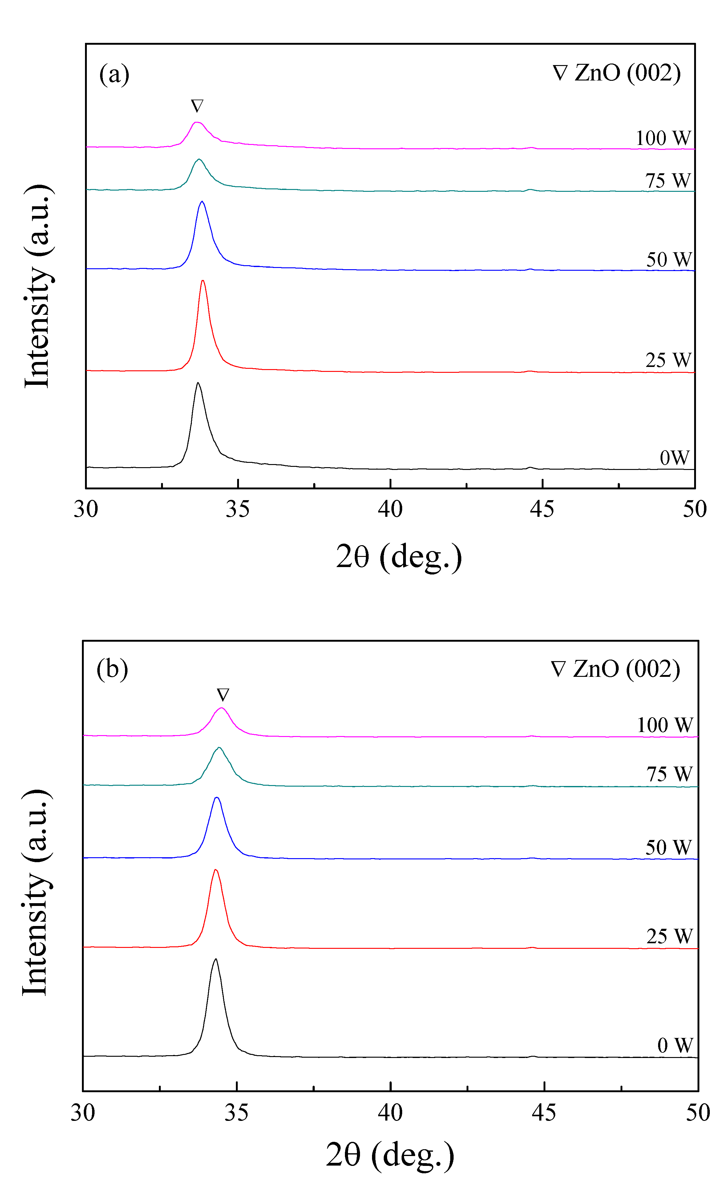
3.1. Composition and Structural Changes of the Mg-Doped AZO Films

Compositions of the as-deposited films analyzed by EDS indicated that the films contained Mg from 1.2 to 3.9 at.% when the film was deposited at the deposition power of Mg target from 25 to 100 W, while fixing the Al–Zn target at 50 W, as presented in Table 1. Mg content increases with increasing the sputtering power of the Mg target.
Figure 1 shows XRD patterns of the as-deposited films and those isothermally annealed at 600 °C. The as-deposited film, which is shown in Figure 1a, had a wurtzite structure (JCPDS 75-0576) with ZnO (002) preferential orientation. No Al2O3 or MgO diffraction peak was observed within the detection sensitivity of the instrument. This preferential orientation implies that the c axis of the Mg-doped AZO grains perpendicularly towards to the substrate surface because the surface energy of (002) plane is the lowest in ZnO wurtzite structure [19]. A similar observation on preferred (002) wurtzite structure for the Mg-doped AZO film can be obtained when the film was deposited using the AZO ceramic target and metallic Mg target [17] although its (002) peak intensity decreases with Mg content. Mg addition seems to degrade the (002) preferential orientation. However, a non-preferential orientation of ZnO could be normally obtained when the film was deposited via reactive magnetron sputtering using a metallic Zn target pasted with Al and Mg foils [16]. Our result shows a strong (002) ZnO texture for the as-deposited film in the studied composition range. Further, the diffraction angle of ZnO (002) (from 33.6° for AZO film to 33.8° for 3.9 at.% Mg-doped AZO film) was slightly lower than that of standard wurtzite structure of ZnO (34.3° from JCPDS 75-0576). This fact indicates that the film may experience a large lattice distortion arising from the lattice expansion at the as-deposited state due to the incorporation of Mg and Al. The MgxZn1−xO film has been found to remain its wurtzite structure when x < 0.36 [20] and Mg-doped AZO films prepared using ceramic targets also show the structure remains unchanged with 4.8 wt.% Mg doping [21]. As a result, the wurtzite structure in this study remains unchanged because the studied concentration of Mg in AZO film ranges from 1.2 to 3.9 at.%.
The diffraction angle of ZnO (002) preferred orientation shifted toward a higher diffraction angle for the films that were annealed at 600 °C, as shown in Figure 1b. This shifted diffraction angle (from 34.3° for 0 at.% Mg to 34.5° for 3.9 at.% Mg) implies that the lattice constant of the Mg-doped AZO film reduces slightly due to the smaller ionic radius of Mg2+ in comparison with that of Zn2+. Furthermore, peak intensity and full-width-at-half-maximum of (002) diffraction gradually decreased with increasing Mg concentration. By using a Debye–Scherer’s formula, the grain size of the film can be estimated to be 27.2 nm for AZO film and 14.5 nm for 3.9% Mg-doped AZO film upon annealing. More Mg atoms incorporated into the AZO seems to yield the film with a smaller grain. The crystallinity and grain size of Cu, Zn, and Ga doped NiO films also reduce with an increase in the doping concentration, due to the difference in the ionic size of the dopants in comparison with the ionic size of Ni2+ ion [22]. Moreover, the coordination number and geometry of ions also need to be taken into consideration. As mentioned, ZnO has a wurtzite structure. The ionic radius for Zn2+ is 0.74 Å and for O2− is 1.40 Å, corresponding to a ratio between Zn2+ and O2− ionic radius of 0.529. This ratio implies that the ZnO structure is in a tetrahedral ionic arrangement, in turns with four nearest neighboring atoms from the crystal structure, i.e., four oxygen atoms surrounded each zinc atom and four zinc atoms surrounded each oxygen atom. The doping atom, Mg (0.72 Å), tends to replace the Zn lattice site and/or part of existing Al atoms (0.53 Å) that has previously replaced Zn lattice sites. Al-incorporation in the ZnO lattice tends to induce more lattice strain due to the difference in the ionic radii between the two ions. While Mg2+ has a comparable ionic radius with Zn2+, Mg-doped is expected to release the lattice strain on replacing Zn atom and/or Al atom in the ZnO lattice.

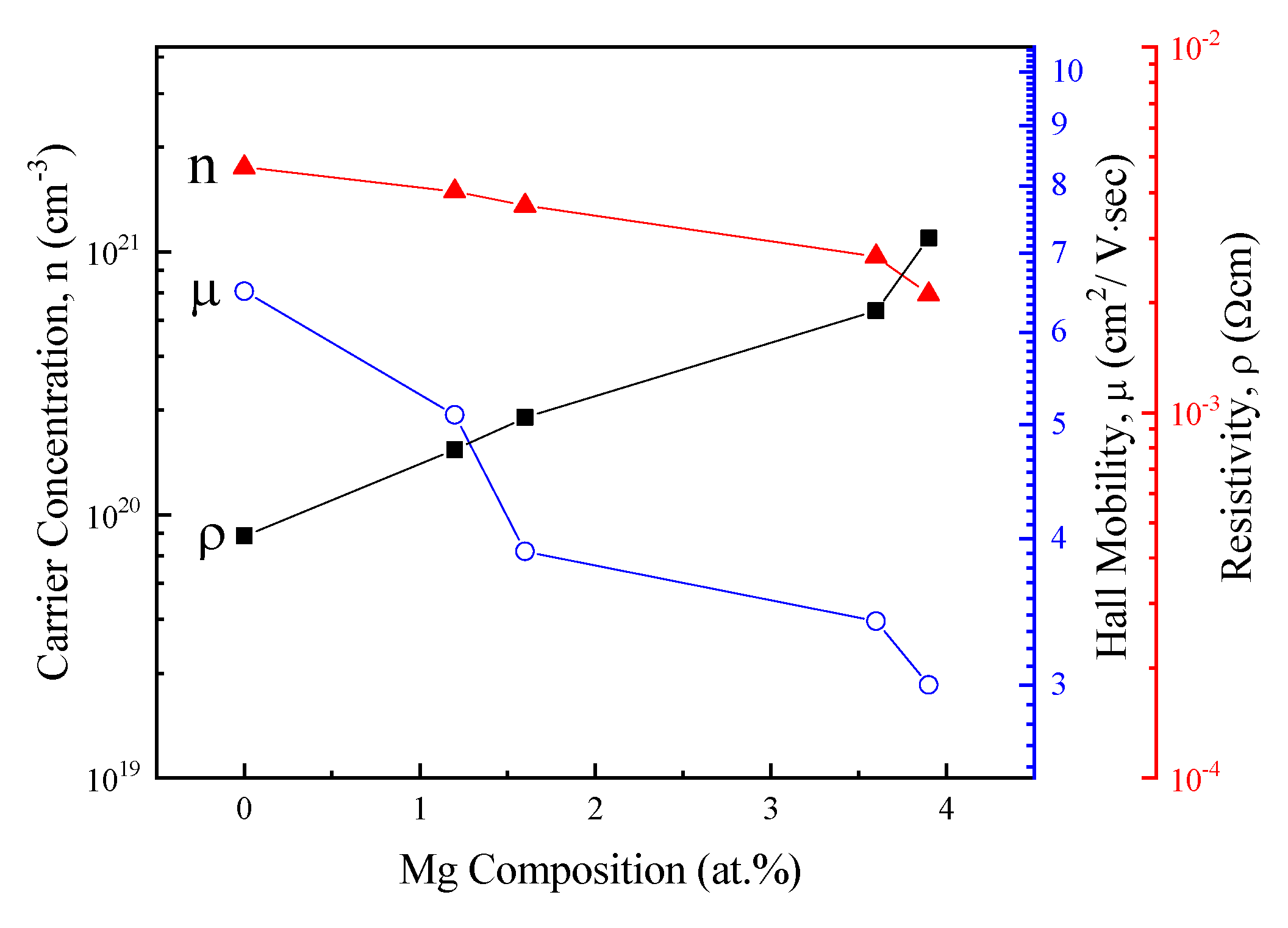
3.2. Electrical Properties of the Mg-Doped AZO Films

Hall effect measurement was used to investigate the electrical properties of the films at room temperature. All of the as-deposited films had a high electrical resistivity (~MΩ) beyond the limit of the instrument, while the electrical resistivity could be significantly reduced after the annealing. The obtained electrical properties of the films post-annealed at 600 °C are shown as a function of the added amount of Mg in Table 2. The variation of the electrical resistivity (ρ), carrier concentration (n), and mobility (μ) of the films is shown in Figure 2 as a function of Mg composition in the AZO film. For the AZO film, carrier concentration was 2.1 × 1021 cm−3, carrier mobility was 6.5 cm2/V sec, and electrical resistivity was 4.6 × 10⁻⁴ Ω·cm, which are comparable with the results in previous studies [23,24]. Mg doping can reduce both of the carrier concentration and mobility, and, thus, increases the electrical resistivity of the film, as shown in Figure 2. The reduction in carrier mobility mostly arises from the high effective mass of Mg (effective mass of electrons in Mg, Al, and Zn is 1.3, 1.2, and 0.85, respectively) which also increases with increasing the Mg content [25]. As a result, a trace amount of 1.2 at.%, Mg-doped AZO film had the lowest electrical resistivity of 7.9 × 10⁻⁴ Ω·cm. Nevertheless, the resultant electrical resistivity in this study is still much lower than those of previously reported Mg-doped AZO films, electrical resistivities in a range of 1.55 × 10⁻¹–1.00 × 10⁻³ Ω·cm deposited using different approaches [2,20,26,27,28], and comparable with the Mg-doped AZO films deposited using sputtering with ceramic targets [29]. Furthermore, the electrical properties of the films in this study are significantly superior to the films deposited on a c-plane sapphire substrate using Zn-Mg and Al targets [27].
Electron mobility is known to be affected by grain boundary scattering, ionized impurity scattering, and alloying scattering. Thus, the effective electron mobility can be represented by the Equation (1) shown, as follows [17]:
1 μ e = 1 μ g b + 1 μ i + 1 μ a
where μe is electron mobility, μgb is mobility caused by grain boundary scattering, µi is mobility due to ionized impurity scattering, and μa is mobility due to alloy scattering. Carrier concentrations of the studied films were ~1021 cm−3, as shown in Table 2, suggesting that the scattering mechanism affected by alloying scattering is negligible [27]. Besides, the films with Mg concentration ≤ 1.6 at.% have a carrier concentration of more than 1021 cm−3, implying that scattering is mostly dominated by ionized impurity scattering where Mg atom is incorporated in lattice site replacing part of the Zn lattice. As the mentioned, atomic radius of Mg (0.72 Å) is only slightly smaller than that of Zn (0.74 Å), suggesting that the doping of Mg, in comparison with Al, generates less lattice strain due to the small lattice mismatch. The structural analysis shown in Figure 1 also confirmed that using a small amount of Mg doping yields the same wurtzite ZnO phase, associated with a slight shift of ZnO (002) orientation toward a higher diffraction angle, corresponding to the smaller ionic radius of Mg2+ in comparison with that of Zn2+. Notably, a trace amount of Al-doped in ZnO also suggests that the substitutional replacing of Zn lattice site in ZnO, although ionic radius of Al3+ (0.53 Å), is much smaller than that of Zn2+ [4]. In this study, Mg atom is also possible to replace the existing Al sites or to occupy interstitial sites in the ZnO lattice. As a consequence, the effect of Al doping in ZnO can be partially offset by Mg because Mg is more atomic size comparable and valance identical. This fact supports that the reduction of carrier concentration with Mg doping shown in Table 2. For Mg concentration ≥ 3.6 at.%, the carrier concentration of the film is slightly less than 1021 cm−3, indicating the scattering mechanism gradually changes to grain boundary scattering because the excess Mg atoms may accumulate at grain boundaries [17,27]. Crystallinity decreases with increasing Mg content, as the XRD pattern shows in Figure 1, also supports the scattering mechanism discussed.
Because of Zn2+ and Mg2+ have the same valence number, the substitution between Mg2+ and Zn2+ should not generate or consume carriers of ZnO [30]. However, Mg and Al may also exist at grain boundaries and retard carriers’ conduction [11,12]. For Mg-doped AZO film, Mg, instead of Al, may replace part of the Zn lattice site in wurtzite ZnO. Doping more Mg leads to a lower carrier concentration because Mg2+ creates fewer carriers than Al3+ [31], and, thus, a higher electrical resistivity for the resultant Mg-doped AZO film.

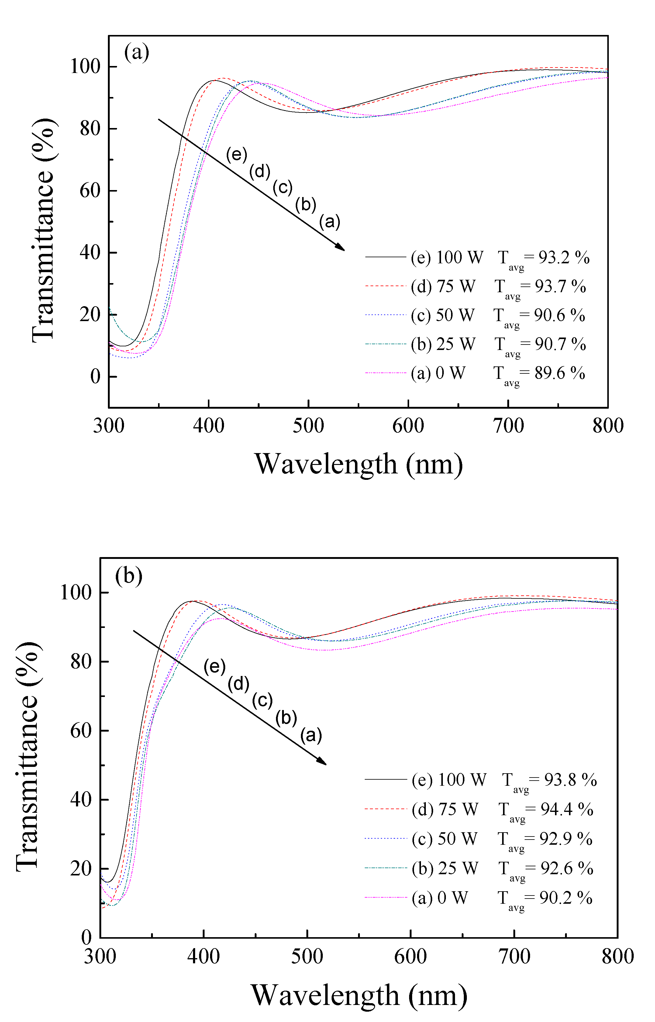
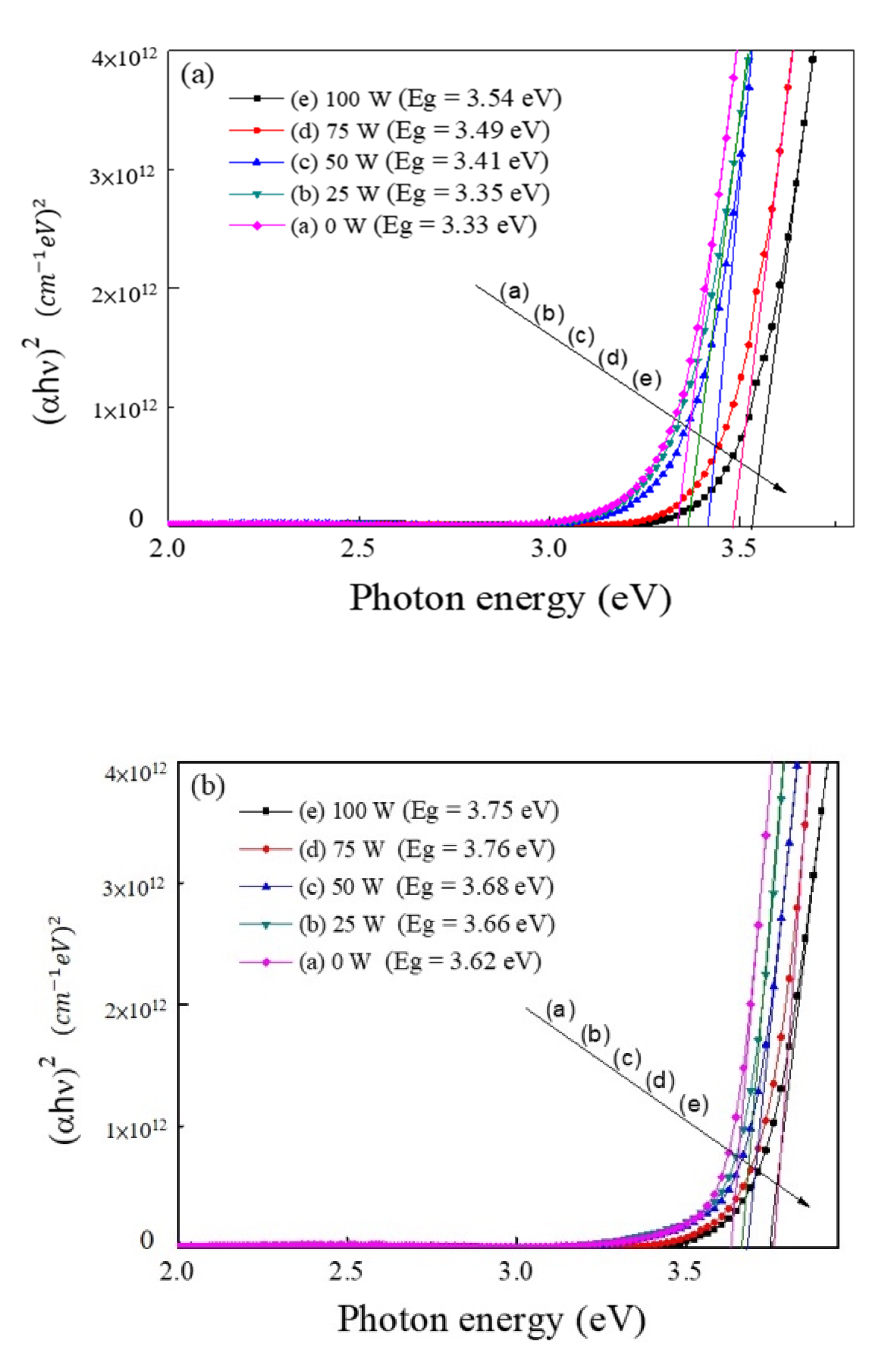
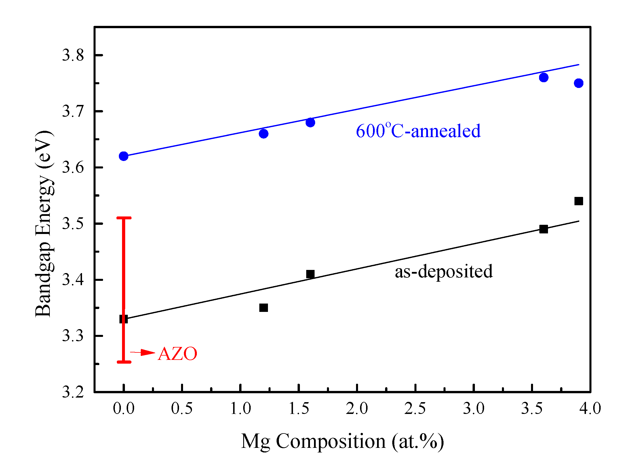
3.3. Optical Transmittance and Bandgap of the Mg-Doped AZO Films

Figure 3 shows the transmittance in the UV-vis-IR regions (300–800 nm) for the films before and after annealing at 600 °C. Optical transmittance of the film, determined as an average value in the visible light range between 400 and 800 nm, was from 89.6% to 93.7% for the as-deposited films (shown in Figure 3a) and from 90.2% to 94.4% for the annealed films (shown in Figure 3b). The films had a higher transmittance in the visible light range than previously reported results (~85%) [16,17,21,28]. The average transmittance increases with Mg concentration due to the reduced carrier concentration from the annihilation of oxygen vacancies [32]. The decrease in carrier concentration also reduces the overlap of the conduction band and therefore widens the bandgap that will be discussed later. A sharp increase in the absorption coefficient occurred at a wavelength of ~400 nm, indicating that the electrons can be excited from a filled band to an empty band by the photoexcitation. Figure 3 also shows that the absorption in the wavelength ranging from 300 to 400 nm shifted toward a short wavelength for the film with a high Mg concentration. The phenomena can be explained by the Burstein–Möss effect [33], in which the bottom of the conduction band might be filled up by the released electrons from oxygen vacancies. ZnO is well known as an intrinsic n-type material and the Fermi level will be of the conduction band when it is doped with Al and Mg. Since the states below the Fermi level of the conduction band are filled, the absorption edge should shift to higher energy [19,34].
The corresponding energy at the onset of this rapid change in the absorption is defined as the optical energy bandgap, Eg [35,36]. To calculate the bandgaps of the films, the absorption coefficient was assumed corresponding to the direct bandgap of wurtzite structured Mg-doped AZO. Plots of (αhν)2 against the photon energy hν, i.e., Tauc’s model equation, where α is the absorption coefficient, h is the Plank’s constant, and v is the photon frequency [37,38], are shown in Figure 4. Sharp absorption edges shifted to a blue light region for the high Mg-doped AZO film, implying an increase in the bandgap energy. The optical bandgap energies determined from the obtained absorption spectra were from 3.33 to 3.54 eV for the as-deposited Mg-doped AZO thin films, as shown in Figure 4a, showing that it increased linearly with increasing Mg dopant concentration. After annealing at 600 °C, the bandgap further increased with increasing Mg concentration from 3.62 to 3.75 eV, as shown in Figure 4b. The obtained results show that the bandgap of Mg-doped AZO thin films is larger than that of pure ZnO thin film (3.27–3.37 eV) [39,40,41] and those of AZO films (3.25–3.51 eV) [4,5], depicting that the remarkable effect of bandgap enlargement by Mg doping.
The widening bandgap by Mg doping in AZO also suggests that Mg is successfully incorporated into the wurtzite ZnO matrix, replacing Zn lattice sites, due to the electronegativity effect and the small difference between the ionic radius. Furthermore, annealing the sample also widens the bandgap of the studied films. Thus, this study shows that the bandgap of AZO thin films can be enlarged through Mg doping for the film deposited by sputtering using metallic targets, whereas the transmittance of AZO films can also be improved simultaneously by Mg doping. The improvement makes the Mg-doped AZO thin film a potential material for applications in optoelectronics UV-light devices.
Using the Vegard’s law EgMg:AZO = (1 − x) EgAZO + x EgMgO and taking EgAZO = 3.33 eV for the as-deposited film, 3.62 eV for the 600 °C-annealed film (Figure 3), and EgMgO = 7.8 eV [28,42] reported previously, the expected variation of the energy band gap of the studied Mg-doped AZO films are consistent with those of the Eg obtained, as shown in Figure 5. Figure 5 also summarizes some of the results reported previously to demonstrate most of the measured bandgap in AZO films prepared by various processes. As shown, Eg of the as-deposited Mg-doped AZO in this study is comparable to the AZO, suggesting that poor crystallinity of the as-deposited film indeed affects the Eg. However, 600 °C-annealed Mg-doped AZO films have a higher Eg than that of the as-deposited state because the incorporated Mg atoms substitute part of the Zn lattice sites, and, thus, enlarge the bandgap energy of the AZO film. Notably, the Vegards’s law needs to be modified with a bowing parameter in terms of EgMg:AZO = (1 − x) Eg AZO + x Eg MgO − bx (1 − x), where b is bowing parameter [43,44]. Since the modification from the bowing parameter is ~0.07 eV for the composition range studied due to lattice distortion and charge exchange by alloying of the ZnO crystal [13], the Eg predicted by Vegard’s law due to modification of the bowing parameter should be negligible.

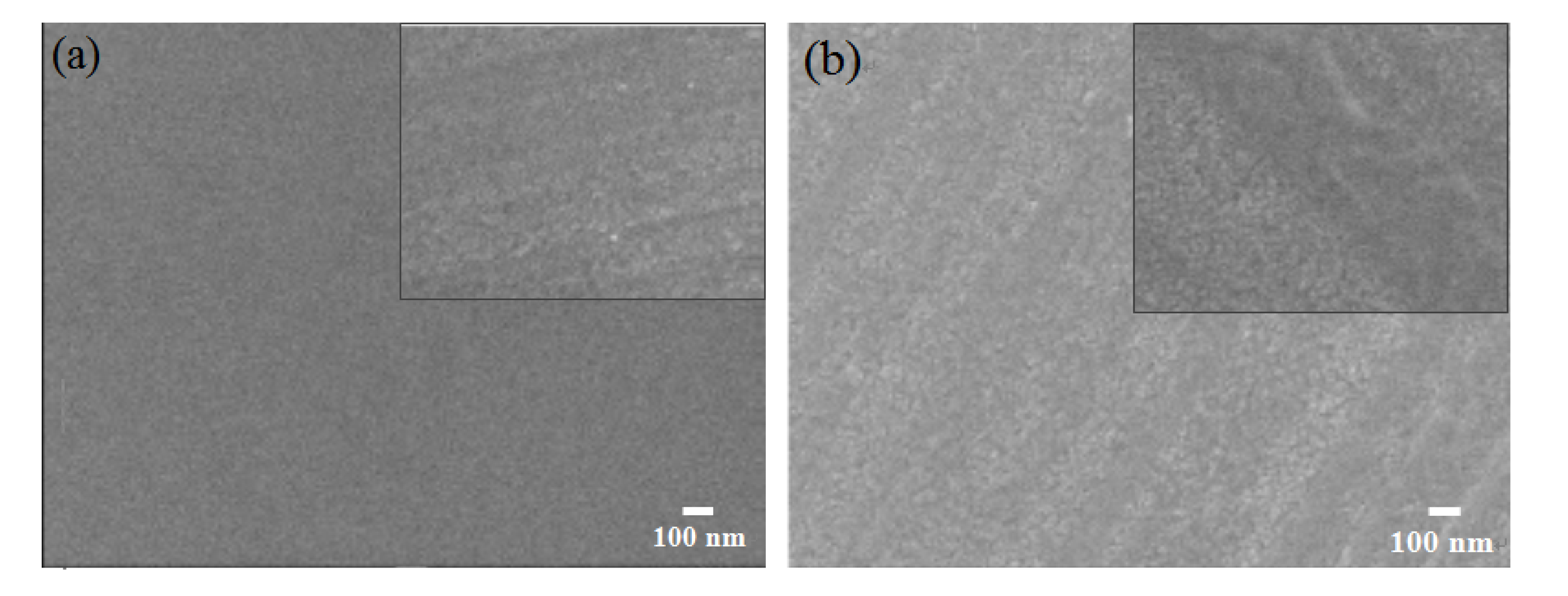
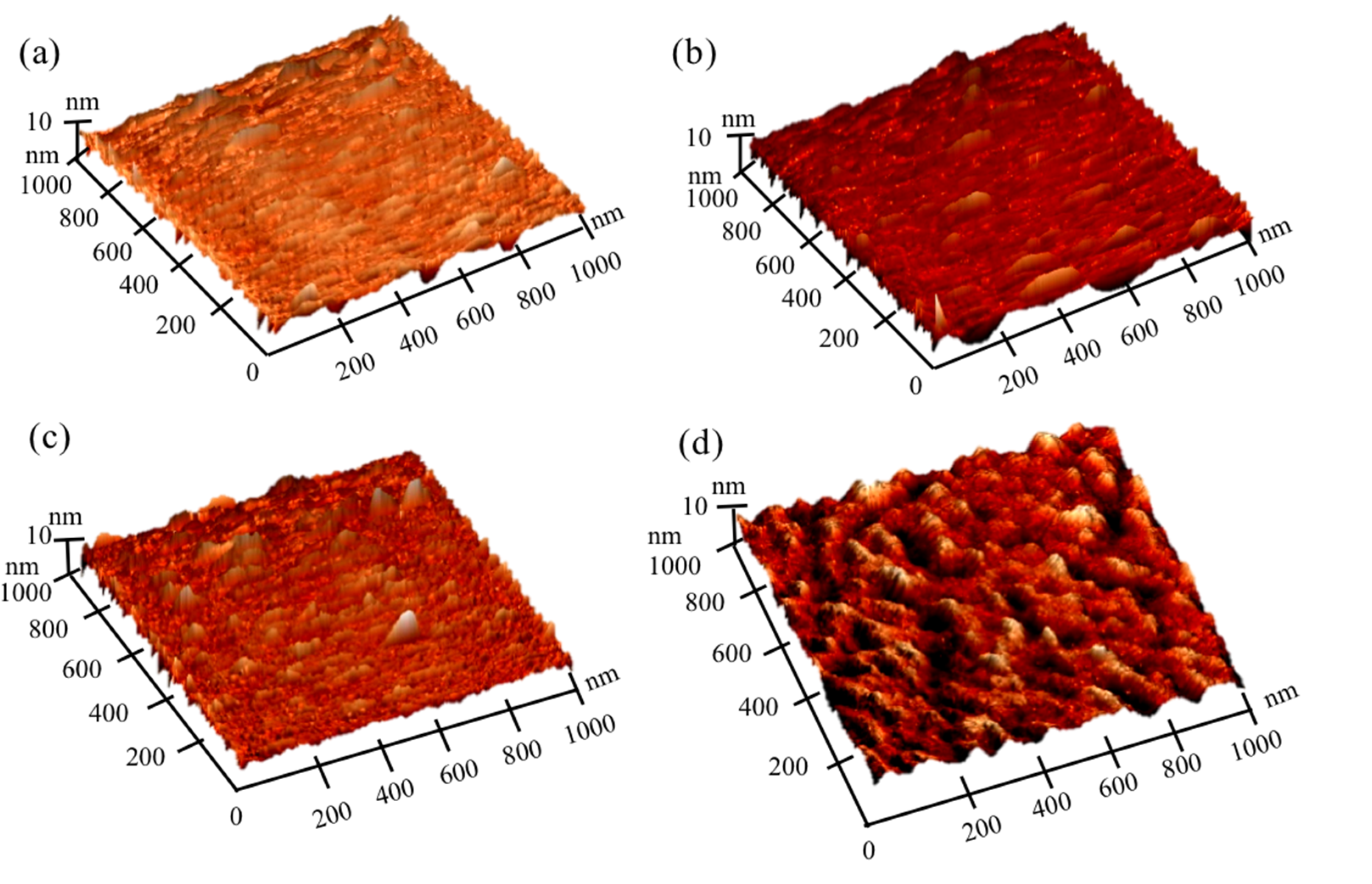
3.4. Surface Morphologies of the Mg-Doped AZO Films

Figure 6 shows the surface morphologies of the representative films before and after annealing at 600 °C. The surface morphology of the as-deposited AZO film is shown in Figure 6a, wherein the film remained smooth after the annealing (inset in Figure 6a). As observed, no obvious grain boundary can be found on the surface of the film, suggesting that the grain is too small to be observed. Surface morphologies of the as-deposited 1.2 at.% Mg-doped AZO film and the film annealed at 600 °C are shown in Figure 6b, indicating that the films also remained smooth. The as-deposited AZO film had a small Ra of 2.3 nm and the annealed film had a Ra of 4.4 nm due to grain growth after the annealing, as AFM images shown in Figure 7a,b, respectively. The 1.2 at.% Mg-doped AZO film also had a smooth surface both for the as-deposited state, with a Ra of 3.4 nm (Figure 7c), and that being annealed at 600 °C, with a Ra of 5.3 nm (Figure 7d). The films have a smooth surface both on the as-deposited state and those isothermally annealed at 600 °C, which is in terms an essential factor for applications in TCOs industry.

4. Conclusions

Structural, optical, and electrical properties of Mg-doped AZO films prepared by the reactive co-sputtering method, using metallic targets of Mg and Al–Zn, were systematically investigated. Mg doping increased effectively in the bandgap energy of AZO from 3.62 to 3.75 eV. Besides, optical transmittances of all the films were over 90% in the visible light region, and all films showed a sharp absorption edge in the UV region. Meanwhile, Mg-doped AZO (002) preferential orientation still preserved after the 600 °C-annealing, demonstrating that dopant of Mg has substituted part of the Zn lattice site. The 1.2 at.% Mg-doped AZO film had the lowest electrical resistivity of 7.9 × 10⁻⁴ Ω·cm, the optical transmittance of 92.6% in the visible light range, and bandgap of 3.66 eV when the film was annealed at 600 °C. The results demonstrate that a superior transparent conductive Mg-doped AZO film can be deposited using metallic targets. This study may provide insight into a potential application of the Mg-doped AZO film as a transparent conducting oxide.

Author Contributions

Organized and designed the experiment procedures, L.-C.Y. and J.-S.F.; executed the film depositions and measurements, D.-R.J., F.-R.P., and C.-H.H. All authors have read and agreed to the published version of the manuscript.

Funding

This work is supported by the Ministry of Science and Technology, Taiwan under grant no. MOST 107-2221-E-150-002-MY2 and experimentally supported by the Common Laboratory for Micro/Nano Science and Technology of National Formosa University.

Conflicts of Interest

The authors declare no conflict of interest.

References

  1. Othmen, W.B.H.; Hamed, Z.B.; Sieber, B.; Addad, A.; Elhouichet, H.; Boukherroub, R. Structural and optical characterization of p-type highly Fe-doped SnO2 thin films and tunneling transport on SnO2:Fe/p-Si heterojunction. Appl. Surf. Sci. 2018, 434, 879–890. [Google Scholar] [CrossRef]
  2. Fernández, S.; Borlaf, F.; García-Pérez, F.; Gómez-Mancebo, M.B.; Munuera, C.; García-Hernández, M.; Elhouichet, H.; Braña, A.F.; Naranjo, F.B. Tailored amorphous ITAZO transparent conductive electrodes. Mater. Sci. Semicond. Proc. 2019, 90, 252–258. [Google Scholar] [CrossRef]
  3. Yaglioglu, B.; Huang, Y.J.; Yeom, H.Y.; Paine, D.C. A study of amorphous and crystalline phases in In2O3–10 wt% ZnO thin films deposited by DC magnetron sputtering. Thin Solid Films 2006, 496, 89–94. [Google Scholar] [CrossRef]
  4. Misra, P.; Ganeshan, V.; Agrawal, N. Low temperature deposition of highly transparent and conducting Al-doped ZnO films by RF magnetron sputtering. J. Alloys Compd. 2017, 725, 60–68. [Google Scholar] [CrossRef]
  5. Mickan, M.; Helmersson, U.; Horwat, D. Effect of substrate temperature on the deposition of Al-doped ZnO thin films using high power impulse magnetron sputtering. Surf. Coat. Technol. 2018, 347, 245–251. [Google Scholar] [CrossRef]
  6. Urper, O.; Baydogan, N. Influence of structural changes on electrical properties of Al:ZnO films. Mater. Lett. 2020, 258, 126641. [Google Scholar] [CrossRef]
  7. Lin, M.; Huang, J.M.; Ku, C.S.; Lin, C.M.; Lee, H.Y.; Juang, J.Y. High mobility transparent conductive Al-doped ZnO thin films by atomic layer deposition. J. Alloys Compd. 2017, 727, 565–571. [Google Scholar] [CrossRef]
  8. Banerjee, P.; Lee, W.J.; Bae, K.R.; Lee, S.B.; Rubloff, G.W. Structural, electrical, and optical properties of atomic layer deposition al-doped ZnO films. J. Appl. Phys. 2010, 108, 043504. [Google Scholar] [CrossRef] [Green Version]
  9. Zhang, W.; Gan, J.; Li, L.; Hu, Z.; Shi, L.; Xu, N.; Sun, J.; Wu, J. Tailoring of optical and electrical properties of transparent and conductive Al-doped ZnO films by adjustment of Al concentration. Mater. Sci. Semicond. Proc. 2018, 74, 147–153. [Google Scholar] [CrossRef]
  10. Gorczyca, I.; Teisseyre, H.; Suski, T.; Christensen, N.E.; Svane, A. Structural and electronic properties of wurtzite MgZnO and BeMgZnO alloys and their thermodynamic stability. J. Appl. Phys. 2016, 120, 215704. [Google Scholar] [CrossRef]
  11. Hu, Y.; Zeng, H.; Du, J.; Hu, Z.; Zhang, S. The structural, electrical and optical properties of Mg-doped ZnO with different interstitial Mg concentration. Mater. Chem. Phys. 2016, 182, 15–21. [Google Scholar] [CrossRef]
  12. Dobrozhan, O.; Diachenko, O.; Kolesnyk, M.; Stepanenko, A.; Vorobiov, S.; Baláž, P.; Plotnikov, S.; Opanasyuk, A. Morphological, structural and optical properties of Mg-Doped ZnO nanocrystals synthesized using polyol process. Mater. Sci. Semicond. Proc. 2019, 102, 104595. [Google Scholar] [CrossRef]
  13. Chen, Y.J.; Brahma, S.; Liu, C.P.; Huang, J.L. Enhancement of the piezoelectric coefficient in hexagonal MgxZn1-xO films at lower Mg compositions. J. Alloys Compd. 2017, 728, 1248–1253. [Google Scholar] [CrossRef]
  14. Jeong, S.H.; Park, J.H.; Lee, B.T. Effects of Mg doping rate on physical properties of Mg and Al co-doped Zn1-x-0.02MgxAl0.02O transparent conducting oxide films prepared by RF magnetron sputtering. J. Alloys Compd. 2014, 617, 180–184. [Google Scholar] [CrossRef]
  15. Song, P.K.; Akao, H.; Kamel, M.; Shigesato, Y.; Yasui, I. Preparation and crystallization of tin-doped and undoped amorphous indium oxide films deposited by sputtering. Jpn. J. Appl. Phys. 1999, 38, 5224–5226. [Google Scholar] [CrossRef]
  16. Wang, C.Y.; Ma, S.Y.; Li, F.M.; Chen, Y.; Xu, X.L.; Wang, T.; Yang, F.C.; Zhao, Q.; Liu, J.; Zhang, X.L.; et al. The effect of Mg and Al co-doping on the structural and photoelectric properties of ZnO thin film. Mater. Sci. Semicond. Proc. 2014, 17, 27–32. [Google Scholar] [CrossRef]
  17. Dhawan, R.; Panda, E. Mg addition in undoped and Al-doped ZnO films: Fabricating near UV transparent conductor by bandgap engineering. J. Alloys Compd. 2019, 788, 1037–1047. [Google Scholar] [CrossRef]
  18. Abed, C.; Fernández, S.; Aouida, S.; Elhouichet, H.; Priego, F.; Castro, Y.; Gómez-Mancebo, M.B.; Munuera, C. Processing and study of optical and electrical properties of (Mg, Al) co-doped ZnO thin films prepared by RF magnetron sputtering for photovoltaic application. Materials 2020, 13, 2146. [Google Scholar] [CrossRef]
  19. Shan, F.K.; Kim, B.I.; Liu, G.X.; Liu, Z.F.; Sohn, J.Y.; Lee, W.J.; Shin, B.C.; Yu, Y.S. Blueshift of near band edge emission in Mg doped ZnO thin films and aging. J. Appl. Phys. 2004, 95, 4772–4776. [Google Scholar] [CrossRef]
  20. Zhao, D.X.; Liu, Y.C.; Shen, D.Z.; Lu, Y.M.; Zhang, J.Y.; Fan, X.W. Photoluminescence properties of MgxZn1-xO alloy thin films fabricated by the sol-gel deposition method. J. Appl. Phys. 2001, 90, 5561–5563. [Google Scholar] [CrossRef] [Green Version]
  21. Park, S.M.; Gu, G.H.; Park, C.G. Effects of Mg doping to optimize properties ZnO: Al for the transparent conductive oxide (TCO). Phys. Status Solidi 2011, 208, 2688–2691. [Google Scholar] [CrossRef]
  22. Manjunatha, K.N.; Paul, S. Wire-bar coating of doped nickel oxide thin films from metal organic compounds. Appl. Surf. Sci. 2019, 488, 903–910. [Google Scholar] [CrossRef]
  23. Chen, H.; Jeong, Y.H.; Park, C.B. Enhancement of electrical properties on ZnO:Al thin film due to hydrogen annealing and SiO2 coating in damp-heat environment. Trans. Electr. Electron. Mater. 2009, 10, 58–61. [Google Scholar] [CrossRef] [Green Version]
  24. Chen, Y.Y.; Hsu, J.C.; Wang, P.W.; Pai, Y.W.; Wu, C.Y.; Lin, Y.H. Dependence of resistivity on structural and composition of AZO films fabricated by ion beam co-sputtering deposition. Appl. Surf. Sci. 2011, 257, 3446–3450. [Google Scholar] [CrossRef]
  25. Kwok, H.L. Electronic Materials, 2nd ed.; PWS Publishing Company: Boston, MA, USA, 1997; pp. 84–85. [Google Scholar]
  26. Matsubara, K.; Tampo, H.; Shibata, H.; Yamada, A.; Fons, P.; Iwata, K.; Niki, S. Band-gap modified Al-doped Zn1-xMgxO transparent conducting film deposited by pulsed laser deposition. Appl. Phys. Lett. 2004, 85, 1374–1376. [Google Scholar] [CrossRef]
  27. Cohen, D.J.; Ruthe, K.C.; Barnett, S.A. Transparent conducting Zn1-xMgxO:(Al, In) thin films. J. Appl. Phys. 2004, 96, 459–467. [Google Scholar] [CrossRef]
  28. Karzazi, O.; Soussi, L.; Louardi, A.; El Bachiri, A.; Khaidar, M.; Monkade, M.; Erguig, H.; Taleb, M. Transparent conducting properties of Mg and Al co-doped ZnO thin films deposited by spray pyrolysis technique. Superlattices Microstruct. 2019, 127, 61–65. [Google Scholar] [CrossRef]
  29. Jeon, K.S.; Suryawanshi, M.P.; Kim, I.Y.; Jang, J.S.; Yun, J.H.; Moon, J.H.; Kim, J.H. Gap characteristics of quaternary mg and Al co-doped ZnO thin films prepared by radio frequency sputtering Method. Sci. Adv. Mater. 2016, 8, 669–674. [Google Scholar] [CrossRef]
  30. Huang, K.; Tang, Z.; Zhang, L.; Yu, J.; Lv, J.; Liu, X.; Liu, F. Preparation and characterization of Mg-doped ZnO thin films by sol–gel method. Appl. Surf. Sci. 2012, 58, 3710–3713. [Google Scholar] [CrossRef]
  31. Duan, L.; Zhao, X.; Zheng, Z.; Wang, Y.; Geng, W.; Zhang, F. Structural, optical and photocatalytic properties of (Mg, Al)-codoped ZnO powders prepared by sol-gel method. J. Phys. Chem. Solids 2015, 76, 88–93. [Google Scholar] [CrossRef]
  32. Kim, J.H.; Jeon, K.A.; Kim, G.H.; Lee, S.Y. Electrical, structural, and optical properties of ITO thin films prepared at room temperature by pulsed laser deposition. Appl. Surf. Sci. 2006, 252, 4834–4837. [Google Scholar] [CrossRef]
  33. Guillén, C.; Herrero, J. Influence of oxygen in the deposition and annealing atmosphere on the characteristics of ITO thin films prepared by sputtering at room temperature. Vacuum 2006, 80, 615–620. [Google Scholar] [CrossRef]
  34. Burstein, E. Anomalous Optical Absorption Limit in InSb. Phys. Rev. 1954, 93, 632. [Google Scholar] [CrossRef]
  35. Kripal, R.; Gupta, A.K.; Srivastava, R.K.; Mishra, S.K. Photoconductivity and photoluminescence of ZnO nanoparticles synthesized via co-precipitation method. Spectrochim. Acta Part A Mol. Biomol. Spectrosc. 2011, 79, 1605–1612. [Google Scholar] [CrossRef] [PubMed]
  36. Manoharan, S.S.; Arora, S. Photoluminescent properties of Mg doped ZnO by microwave combustion and microwave polyol method. Mater. Sci. Eng. B 2009, 162, 68–73. [Google Scholar] [CrossRef]
  37. Tauc, J. Optical properties and electronic structure of amorphous Ge and Si. Mater. Res. Bull. 1968, 3, 37–46. [Google Scholar] [CrossRef]
  38. El Hallani, G.; Nasih, S.; Fazouan, N.; Liba, A.; Khuili, M.; Sajieddine, M.; Mabrouki, M.; Laanab, L.; Atmani, E.H. Comparative study for highly Al and Mg doped ZnO thin films elaborated by sol gel method for photovoltaic application. J. Appl. Phys. 2017, 121, 135103. [Google Scholar] [CrossRef]
  39. Lee, K.E.; Wang, M.; Kim, E.J.; Hahn, S.H. Structural, electrical and optical properties of sol–gel AZO thin films. Curr. Appl. Phys. 2009, 9, 683–687. [Google Scholar] [CrossRef]
  40. Yao, P.C.; Hang, S.T.; Lin, Y.S.; Yen, W.T.; Lin, Y.C. Optical and electrical characteristics of Al-doped ZnO thin films prepared by aqueous phase deposition. Appl. Surf. Sci. 2010, 257, 1441–1448. [Google Scholar] [CrossRef]
  41. Vishwas, M.; Rao, K.N.; Phani, A.R.; Gowda, K.V.A.; Chakradhar, R.P.S. Optical, electrical and structural characterization of ZnO:Al thin films prepared by a low cost sol–gel method. Solid State Commun. 2012, 152, 324–327. [Google Scholar] [CrossRef]
  42. Zhuang, H.; Wang, J.; Liu, H.; Li, J.; Xu, P. Structural and optical properties of ZnO nanowires doped with magnesium. Acta Phys. Pol. 2011, 119, 819–823. [Google Scholar] [CrossRef]
  43. Bernard, J.E.; Zunger, A. Electronic structure of ZnS, ZnSe, ZnTe, and their pseudobinary alloys. Phys. Rev. B 1987, 36, 3199–3228. [Google Scholar] [CrossRef] [PubMed]
  44. Wei, S.H.; Zhang, S.B.; Zunger, A. First-principles calculation of band offsets, optical bowings, and defects in CdS, CdSe, CdTe, and their alloys. J. Appl. Phys. 2000, 87, 1304–1311. [Google Scholar] [CrossRef] [Green Version]
Figure 1. X-ray diffraction system (XRD) spectra of the Mg-doped AZO thin films (a) before and (b) annealed at 600 °C for 5 min.
Coatings 10 00708 g001
Figure 2. Variations of the electrical resistivity (ρ), carrier concentration (n), and mobility (µ) of the films annealed at 600 °C.
Coatings 10 00708 g002
Figure 3. Optical transmission spectra for the studied film (a) as-deposited state and (b) post-annealed at 600 °C.
Coatings 10 00708 g003
Figure 4. The (αhν)2 versus hν plots of the studied films (a) as-deposited state and (b) isothermally annealed at a temperature of 600 °C.
Coatings 10 00708 g004
Figure 5. Summary of bandgap obtained for Mg-doped AZO films with different Mg doping concentrations. Solid lines present the bandgap trend predicted by Vegard’s law; the red line is the bandgap of AZO referred to the literature.
Coatings 10 00708 g005
Figure 6. Surface images of (a) as-deposited AZO thin film and (b) as-deposited 1.2 at.% Mg-doped AZO film; inset shows the surface morphology of the respective film post-annealed at 600 °C.
Coatings 10 00708 g006
Figure 7. AFM images of (a) as-deposited AZO film, (b) AZO film that being annealed at 600 °C, (c) as-deposited 1.2 at.% Mg-doped AZO film, and (d) 1.2 at.% Mg-doped AZO film that being annealed at 600 °C.
Coatings 10 00708 g007
Table 1. Composition of the studied films examined by energy dispersive spectroscopy (EDS).
Mg Deposition Power (W)Mg (at.%)Al (at.%)Zn (at.%)O (at.%)
001.851.746.5
251.21.752.744.4
501.61.850.646.0
753.61.644.550.3
1003.91.542.951.7
Table 2. Electrical properties of the films annealed at 600 °C.
Mg Composition (at.%)Carrier Concentration (cm−3)Mobility (cm2/Vsec)Resistivity (Ω·cm)
02.1 × 10216.54.6 × 10−4
1.21.7 × 10215.17.9 × 10−4
1.61.5 × 10213.99.7 × 10−4
3.69.6 × 10203.41.9 × 10−3
3.96.9 × 10203.03.0 × 10−3

