

Abstract
A closed-cell metamaterial absorber (CCMA) made of a low-permittivity dielectric is proposed and investigated in this paper. It realizes five absorption peaks below −10 dB in the range of 6–18 GHz, and the strongest absorption can reach near −40 dB. By investigating the distribution of electromagnetic fields, it is found that multi-resonance is caused by the embedding of closed cells. Interestingly, it is possible that part of the absorption peaks could be moved individually by different parameters of the closed-cell arrays. Similarities between the results of experiment and simulation confirm the practical feasibility of the CCMA.
Export citation and abstract BibTeX RIS
Artificial metamaterial absorbers (MAs) have received a lot of attention in recent years because of their outstanding properties in the stealth field. They show excellent flexibility in manipulating electromagnetic waves by structural design. Early on, artificial metal structure (MS) like split ring resonators (SRRs) have realized electromagnetic resonance with negative permittivity.1–4) Based on this revelation, more and more MAs based on MS-like multi-gap SRRs,5) donut-shaped resonators,6) copper rings,7) metallic dishes,8) circular sector resonators,9) closed-meander-wire resonators10) and meander wires11) have been reported. In addition, MSs in combination with traditional materials show excellent absorbing properties.12–17) However, MSs have some defects such as processing difficulty, easy corrosion and high cost, which limit their application prospects.
Some researchers have begun to change their research route to find new MAs. Liu et al.18–20) proposed a series of metamaterial perfect absorbers based on the concept of Mie resonances. Those MAs, which realize one or two absorption bands, are composed of dielectric cubes (115 ≤ ε ≤ 1600) and a metallic ground plane. Similarly, Li et al.21) reported an MA based on E-shaped all-dielectric resonators (ε = 300). And Li et al.22) designed a two-stacked square-shaped strontium titanate (300 ≤ ε ≤ 500). Both of their designs achieved good performance, which were based on Mie resonance theory.23) When Mie resonance generates in dielectric particles, the effective permeability is negative.24–26) This phenomenon was also verified by the work of other researchers. Peng et al.27) investigated a dielectric resonator array made of ceramic (ε = 600), which exhibited left-handed behavior. In addition, isotropic negative permeability resulting from Mie resonance was demonstrated in an array of dielectric ceramic cubes (ε = 1600) reported by Zhao et al.28) The above dielectric MAs consisted of ceramic materials with high permittivity. However, ceramic materials have the disadvantages of heavy weight and high brittleness, which cannot meet the requirements of absorbing materials. In order to avoid these problems, Yu et al.29) proposed a frequency-selective surface based on low-permittivity dielectric (LPD) metamaterials with high strength and low cost. And Cheng et al.30) designed a periodic silicon cross nanostructure array (ε = 11.9). Their works confirmed that electromagnetic resonance could be achieved in LPDs with periodic arrays. This inspired us to make more attempts in the stealth field.
Our group has proposed a series of MAs based on LPDs including hole arrays31,32) and a cross-shaped array.33) These MAs can realize two to six absorption bands, which prove the feasibility of LPDs in the field of stealth. However, these structures consist of edges and corners, which have some obvious limitations due to their porous structure, because smooth surfaces are required in many applications. In the present work, a closed-cell MA (CCMA) based on an LPD is proposed, which has a smooth surface and excellent performance with multiple absorption peaks below −10 dB in the range of 6–18 GHz. It is a closed-cell structure to inspire multimode resonance in the dielectric plate.
Figure 1(a) shows the CCMA unit under consideration. FR-4 is selected for its low permittivity (εr = 4.8, tan δ = 0.025) and high strength. Both the length and width of the CCMA unit are 30 mm (a = 30 mm), and the height is 8 mm (z = 8 mm) without the PEC plate. Periodic closed-cell arrays are distributed in the FR-4 plate, where the length of the side is b = 18 mm, the height is z2 = 4.1 mm, and the distance from the PEC plate is z1 = 3 mm. As we all know, a PEC plate is used as a reflective plate, which can fully reflect electromagnetic waves. Therefore, the absorption can be calculated as A(ω) = 1–∣S11(ω)∣2, where S11(ω) is the reflection index. The S11(ω) of the CCMA is shown in Fig. 1(b). It shows five absorption peaks below −10 dB at 7.776 GHz (f1), 8.496 GHz (f2), 9.968 GHz (f3), 12.768 GHz (f4) and 16.704 GHz (f5) in the range of 6–18 GHz. And the values of S11(ω) are −28.091 dB, −37.932 dB, −14.027 dB, −13.45 dB, and −17.999 dB, respectively. The MA is simulated using the commercial software CST Microwave Studio, which is based on the finite-integration frequency-domain method. In the simulation, both the x- and y-directions are arranged with the periodic boundary conditions, while the z-direction is set as the open space. In the current model, the electromagnetic wave propagates perpendicularly from the +z-direction to the x–y plane. In addition, only the absorption performance of the TE polarization mode is shown here due to structural symmetry along the x–y axis.

Fig. 1. (Color online) (a) Schematic of the CCMA unit. (b) Simulated reflection spectra of the absorber, where f1 = 7.776 GHz, f2 = 8.496 GHz, f3 = 9.968 GHz, f4 = 12.768 GHz and f5 = 16.704 GHz.
Download figure:
Standard image High-resolution imageTo understand the physical mechanism behind multi-band absorption, electric field distributions are investigated at these resonance frequencies, as shown in Fig. 2. The coordinate origin is set at the bottom of the FR-4 plate unit center, as shown in Fig. 1. Owing to the existence of closed-cell arrays, the electromagnetic field changes, which is analyzed by capturing the plane with strong resonance. At f1, f2 and f3, the enhanced electric fields are mainly concentrated around the closed cell. So, the plane (z = 5 in the vertical direction) is captured, as shown in Figs. 2(a)–2(c) respectively. As we can see, at f1, on the E–o–H plane, the enhanced electric fields are distributed in four corners of the unit between two closed cells. The electric fields at f2 are mainly enhanced in the center of the unit in Fig. 2(b). The distributions in Fig. 2(c), at f3, show that enhanced electric fields exist in the center and four corners of the closed cells. At f4 and f5, strong resonances are distributed in the upper and lower parts of the FR-4 plate. Figure 2(d) shows that the electric fields are enhanced near the boundary of the unit. And there are locations of enhanced electric fields in the center and four corners of the unit in Figs. 2(e)–2(g).
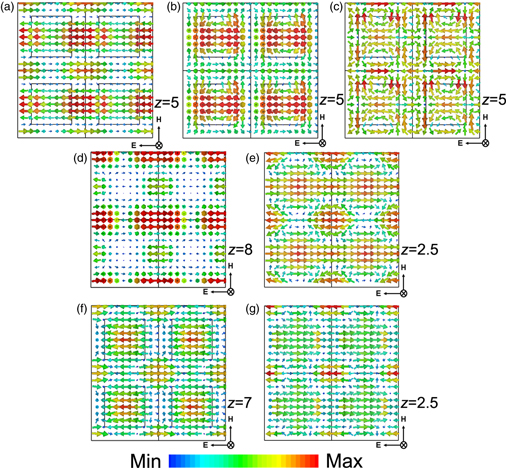
Fig. 2. (Color online) Electric field distributions in the CCMA at (a) f1 (z = 5 mm), (b) f2 (z = 5 mm), (c) f3 (z = 5 mm), (d) f4 (z = 8 mm), (e) f4 (z = 2.5 mm), (f) f5 (z = 7 mm) and (g) f5 (z = 2.5 mm). E and H denote the electric and magnetic field directions, respectively. The maximum electric intensity is 3000 V m−1.
Download figure:
Standard image High-resolution imageFor a better illustration of the absorption inside the CCMA, power loss density (PLD) distributions at five absorption frequencies are clearly shown in Fig. 3. PLD is mainly concentrated on four corners of the unit and between two closed cells, at f1 [Fig. 3(a)]. At f2 and f3, PLD is mainly distributed in the center of the unit [Figs. 3(b)–3(c)]. And there are two floors of enhanced PLD along the dielectric structure at f4 and f5 [Figs. 3(d)–3(e)]. The enhanced PLD is distributed near the boundary of the unit in Fig. 3(d), as well as in the center and four corners of the unit in Fig. 3(e). It shows that the locations of strong energy loss exactly match the locations of enhanced electric fields by comparison. Therefore, it is certain that electric field resonance is an important mechanism that causes electromagnetic wave absorption for CCMAs.
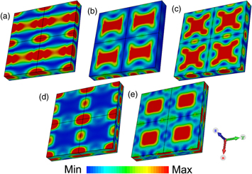
Fig. 3. (Color online) PLD distributions in the CCMA at (a) f1, (b) f2, (c) f3, (d) f4 and (e) f5. The maximum PLD is 2 × 10⁵ W m−3.
Download figure:
Standard image High-resolution imageFurther, the distributions of the electric and magnetic fields in the vertical direction (the direction of wave vector k) will be discussed to explore the principle of wave absorption. Figure 4 shows five groups of figures. The first two figures of every group are strong electric field distributions captured in the planes of x = 0 and x = 15, and the third one is the corresponding sections of magnetic field distributions. Enhanced electric fields are shown in the planes of x = 0 and x = 15 marked by purple and blue lines, respectively, in Fig. 4(a). There are corresponding magnetic field rings in the plane of y = 15 marked by purple and blue rings respectively. These rings are named magnetic dipoles. Magnetic dipoles are formed in the plane of y = 0 in Figs. 4(b) and 4(c). Figures 4(d) and 4(e) show two magnetic dipoles in the direction of wave vector k. It is found that the number of magnetic dipoles increases with the increase of the frequency in the direction of k. It can be explained by standing wave theory. According to the theory, resonances are formed by incident and reflected waves at the interface of two media.33–35) When the thickness of the dielectric is an odd multiple of a quarter of the wavelength, the excitation field can form a stable standing wave in the dielectric.36,37) The wavelength λ of the standing wave and the wavelength l of the incident electromagnetic wave satisfy the following formula:

With the increase of the frequency, the wavelength of the standing wave becomes shorter. So, the electromagnetic wave with higher frequency can induce multi-resonance in the direction of k. In other words, electromagnetic wave absorption is caused by electric resonance formed between the air–dielectric interface and the dielectric–PEC interface.

Fig. 4. (Color online) Field distributions in the CCMA: (a) f1, (b) f2, (c) f3, (d) f4, (e) f5. The maximum electric intensity is 3000 V m−1 and the maximum magnetic intensity is 9 A m−1. The first two figures of every group show the electric field distributions captured in the planes of x = 0 and x = 15, and the third one is the corresponding sections of magnetic field distributions.
Download figure:
Standard image High-resolution imageIn order to study the influence of every parameter on the absorption peaks, different reflection spectral curves are drawn by changing one parameter at a time, when other parameters are fixed. Increasing the parameter a from 30 mm to 32 mm causes the absorption peaks to undergo a red-shift and changes their intensity as well [Fig. 5(a)]. In Fig. 5(b), as the parameter b increases from 18 mm to 22 mm, f1, f2 and f3 show obvious blue-shifts, but f4 and f5 just change a little. This phenomenon can be explained by the electric field distributions in Figs. 2(d)–2(g). Because the enhanced electric field mainly exits in the upper and lower parts of the FR-4 plate, the change of b does not have a heavy effect on the electric field. There is a red-shift of absorption peaks as the parameter z increases from 8 mm to 9 mm [Fig. 5(c)]. The increase of z means the increase of distance between the air–dielectric interface and the dielectric–PEC interface. So, the wavelength of the standing wave could be increased. By the same token, f4 and f5 are more affected by the change of z1 due to the position of the electric resonance [Fig. 5(d)]. And just because, at f4, there is no electric resonance above the closed hole, it has no effect with the increase of z2 [Fig. 5(e)]. It is possible that part of the absorption peaks could be moved by controlling the corresponding parameters of the closed-cell arrays. Figure 5(f) shows a red-shift when εr is increased. It can be explained by the effective medium theory shown in the following formula:38)

where the polarization factor  and
and  and
and  denote the relative permittivity of the host medium and inclusion, respectively. f denotes the volume fraction occupied by the dielectric. Obviously, εr is proportional to
  and inversely proportional to absorption frequency. And the change of other parameters results in the change of the volume fraction, which causes the shift of the absorption peaks.
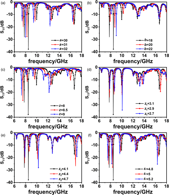
Fig. 5. (Color online) Simulated reflection spectral curves for the CCMA with varying values of different parameters: (a) a, (b) b, (c) z, (d) z1, (e) z2, and (f) εr.
Download figure:
Standard image High-resolution imageWe then carry out simulation and experimental analyses of the proposed CCMA. For the measurement, a CCMA with a size of 300 mm × 300 mm is fabricated using a computer numerical control (CNC) engraving machine (Guangzhou Seahawn Industrial Robotics Co., Ltd.). The precision of the industrial-grade CNC engraving machine is 0.1 mm. To prepare a structure with a closed cell, a hole array is firstly carved on a board of FR-4 (the thickness is 7.1 mm). Then, a board of FR-4 (thickness is 0.9 mm) is glued on top of it [Fig. 6(a)]. The glue is epoxy with low permittivity. Measurement is performed using an NRL arch reflectivity test system (where a vector network analyzer AV3629 connects two speakers) in an electromagnetic microwave chamber. The measured and simulated reflection spectra in the range of 2–18 GHz are obtained, shown in Fig. 6(b), suggesting that the measured spectrum has a similar absorption property to the simulated one. The measured reflection spectra are shown in Fig. 6(c), which have four absorption peaks around 7.8 GHz (−5.58 dB), 8.4 GHz (−10.02 dB), 9.84 GHz (−4.45 dB) and 12.9 GHz (−4.48 dB), entirely consistent with the simulation result. However, there are two obvious discrepancies between the simulation and test results: (1) the measured reflection spectra at f5 do not match the simulated ones; (2) the intensity of every experimental absorption peak is weaker. According to our previous work, the mismatch can be blamed on the fact that the absorption property at high frequency (GHz) is sensitive to experimental errors like an uneven distribution of permittivity and structural deviations.33) All of the experimental errors originating from the fabrication and measurement processes can be summarized as follows: (1) unavoidable machining errors and fillet errors; (2) difficulty in obtaining an FR-4 whose electromagnetic parameters are fully fit for the parameters of the simulation. It should be noted that the two layers of the FR-4 are glued together, which is bound to result in errors. Although like this, we believe that this result is enough to exhibit the novelty and practical feasibility of the proposed CCMA.

Fig. 6. (Color online) (a) Front and back views of the fabricated CCMA prototype and (b) experimental reflection spectral curves.
Download figure:
Standard image High-resolution image
In this work, a CCMA based on an LPD is proposed and investigated. By embedding periodic closed-cell arrays in the layer of LPD, the CCMA achieves five absorption peaks below −10 dB in the range of 6–18 GHz. The phenomenon that a layer of closed-cell arrays can achieve multiple frequencies is caused by multimode resonance between the dielectric–PEC interface and the air–dielectric interface. Simultaneously, it is found that different absorption peaks can be flexibly controlled by changing the lattice dimensions of the closed cell because of the different positions of the corresponding resonance. We believe that the proposed design will provide a cheap and convenient solution to realize multi-band microwave absorbers. It will be useful in the electromagnetic energy harvesting and stealth fields.
Acknowledgments
The work was supported by the Science and Technology Plan Project of Hunan Province (Grant No. 2015TP1007); Initial Research Funding for Special Associate Professor by Central South University (Grant No. 202045002); the National Natural Science Foundation for Young Scientists of China (Grant No. 51802353); Fundamental Research Funds for the Central Universities of Central South University (Grant No. 2018zzts330); and the Opening Foundation of the State Key Laboratory of Metamaterial Electromagnetic Modulation Technology (Grant No. GYL08-1443).