1. Introduction
The increasing global demand for energy, limited fossil fuel supplies on the planet, and global climate changes due to greenhouse gas emissions from fossil fuel burning have made it necessary to use renewable, clean energy sources as energy alternatives. Among the various technologies available, photovoltaics is considered one of the cleanest ways to achieve this objective. However, the difficult task of solar cell manufacturers is to reduce production costs in relation to the resulting output power of the solar modules with a view to enhance their marketability and use. In order to solve this problem, a number of materials have been studied for their use in applications based on solar energy. Among them, recent studies have shown that cuprous oxide (Cu
2O) has become a key candidate, as it has the potential to meet global demand for electricity and reduce photovoltaic costs compared to other materials [
1].
Copper (I) oxide generally exhibits
p-type behavior due to an acceptor level at 0.4 eV above the valence band generated by copper ion vacancies. Donor levels were also observed in Cu
2O due to oxygen vacancies at 0.38 eV below the bottom of the conduction band, showing the existence of Cu
2O with
n-type conductivity [
2]. Cu
2O has a direct band gap of approximately 2 eV, which is within the range appropriate for photovoltaic applications. The high optical absorption coefficient, the simplicity of composition, and its environmentally friendly characteristics have made this semiconductor an attractive material for low-cost solar energy applications [
3]. However, improving the conversion efficiency of Cu
2O-based solar cells remains a major challenge. The highest conversion efficiency achieved with Cu
2O as the active layer is 8.1% with a MgF
2/Al-doped ZnO/Zn
0.38Ge
0.62-O/Cu
2O:Na
p-n heterostructure, showing that further studies are necessary to push the efficiency of Cu
2O-based solar cells toward their theoretical efficiency, which is about 20% [
4,
5]. Typically, p-n heterojunction solar cell structures require
p-type and
n-type semiconductors, which should have proper energy level alignment to improve charge separation and reduce electron-hole recombination. This requirement restricts the choice of selecting the two semiconductor materials. Furthermore, the formation of a
p-n heterojunction leads to a possible lattice mismatch between the two semiconductors, causing a high density of defects at the heterojunction interface, which can act as recombination centers that suppress the separation of electrons and holes and thus impair the performance of the device [
6]. One of the main challenges for the production of Cu
2O-based solar cell devices is the fabrication of Cu
2O
p-n homojunctions. Since the homojunction should not present any interfacial deformation resulting from the lattice mismatch between
p-type and
n-type materials, the separation of photoinduced charges in the Cu
2O homojunction can be considerably improved, hence improving the photoelectric conversion performance [
7]. Another advantage of the homojunction structure is that it will have a higher stability in thermal cycles and higher resistance to cosmic radiation [
8]. Consequently, homojunctions lead to better performance compared to heterojunctions in their applications.
However, research on the fabrication of Cu
2O homojunctions to date is insufficient due to the lack of studies on the production of
n-type Cu
2O films. Since the demonstration of the growth of
n-type Cu
2O films using the electrodeposition method by Siripala et al. in 1986 [
9], several other methods have been reported on preparation of
n-type Cu
2O films on various substrates [
10,
11,
12,
13]. Consequently, a few studies on homojunctions based on Cu
2O films have been reported in the literature. For example, Wang et al. reported the fabrication of Cu
2O
p-n homojunctions. However, their properties as potential solar cell devices have not been addressed [
10]. Later, Han et al. fabricated a Cu
2O
p-n homojunction solar cell with a conversion efficiency of 0.1% by electrochemical growth of a
p-type Cu
2O film using a lactate bath on an
n-type Cu
2O film, which was grown using an acetate bath [
11]. At the same time, Jayathilaka et al. reported the fabrication of Cu
2O
p-n homjunctions in a simpler two-step electrodeposition process using an acetate bath [
14]. Later, McShane and coworkers [
15] fabricated Cu
2O
p-n homojunction solar cells by consecutive electrochemical deposition of a
p-Cu
2O layer, followed by an
n-Cu
2O layer, using the combination of acetate and lactate baths. Initially, the resulting solar cell had a conversion efficiency of 0.29%, which was then improved to 1.06% by improving the front contacts [
16]. Hsu et al. [
17] succeeded in fabricating a homojunction with an efficiency of 0.42% by optimizing the
n-type and
p-type Cu
2O film thickness. Yu et al. [
18] successfully fabricated Cu
2O homojunction by
n-type F-doped Cu
2O and intrinsic
p-Cu
2O, but the highest conversion efficiency of these structures was limited to 0.335%. Recently, Wijesundara et al. [
19] reported the fabrication of Cu
2O homojunctions by electrodeposition in an acetate bath with an efficiency of 0.89%. A Cu
2O
p-n homojunction solar cell with an efficiency of 2.05% was fabricated by Elfadill et al. using a Cl-doped
n-type Cu
2O film and an optimized Na-doped Cu
2O film [
20]. So far, the highest efficiency of 4.21% has been reported on a Cu
2O
p-i-n homojunction solar cell, which was fabricated using a Mn-doped i-type electrodeposited Cu
2O film and a Na-doped thermally oxidized Cu
2O film [
21]. However, in the previously mentioned studies, the open-circuit voltage of the Cu
2O
p-n homojunction was much lower than the theoretically expected value, which is estimated based on the bandgap of Cu
2O [
5]. These studies therefore demonstrate the need to further improve the performance Cu
2O
p-n homojunction solar cell devices.
The performance of the solar cell depends on a number of factors, including the quality of the individual film, the choice of the front and back contacts, and the interfaces between the individual layers. The film processing techniques determine the copper oxide film quality and the optoelectronic properties [
22]. One way to enhance the efficiency is to improve the quality of the
n-type and
p-type surface and interface of the
p-n junction. It has been shown that electrodeposition process can be used to effectively control Cu
2O film parameters during their deposition. However, electrodeposited films have a polycrystalline nature. It is known that the fabricated solar cells have various defects, and these defects can reduce the performance and efficiency of solar cells under certain operating conditions [
23,
24]. In polycrystalline cuprous oxide films containing nonnegligible amounts of traps, the surface recombination plays a notable role in charge extraction and resulting device efficiencies [
25,
26]. Recent studies have shown that this problem can be circumvented by sulfur passivation of Cu
2O films using (NH
4)
2S treatment, which modifies the surface of
n-type and
p-type Cu
2O thin films [
27,
28,
29].
In this study, n-Cu2O/p-Cu2O homojunction solar cells were fabricated via electrodeposition on Ti substrates where orientation of the polycrystalline grains was controlled by varying the pH of the electrolyte to improve the interface between n-type and p-type layers. First, the structural and optical properties of individual films were examined. Then, the structural, optical, and electrical properties of the resulting n-Cu2O/p-Cu2O solar cell structure were examined. Subsequently, sulfur treatment and annealing were successfully used to improving the efficiency of Ti/n-Cu2O/p-Cu2O/Au solar cells.
2. Materials and Methods
Initially, Cu
2O thin films were potentiostatically electrodeposited using a potentiostat (Hokoto Denko HAB-151, Hokuto Denko, Atsugi, Kanagawa, Japan) on Ti substrates (area: −2 cm × 1 cm; thickness: −0.2 mm) that were cleaned with detergent, diluted with HNO
3 in an acetone bath, and diluted with distilled water prior to electrodeposition. The reference and counter electrodes were saturated calomel electrode (SCE) and a Pt sheet, respectively. All chemicals used in the experiments were of reagent grade. In order to fabricate a
p-n homojunction,
n- and
p-type Cu
2O films were sequentially electrodeposited in two different electrolyte solutions. In the first step,
n-type Cu
2O films were electrochemically deposited on a Ti substrate in an acetate bath that contained an aqueous solution of 0.01 M of copper acetate and 0.1 M of sodium acetate (Acetate bath) [
27]. The deposition was made at a potential −200 mV vs. SCE at a bath temperature of 60 °C for 20 min. The pH of the acetate bath was adjusted in the range of 5.5–6.5 at 0.1 increments to find out the best photoactive sample. Then a
p-Cu
2O film was directly deposited on the highly photoactive
n-Cu
2O film at the deposition potential −400 mV vs. SCE and a bath temperature of 60 °C in a lactate bath that contained an aqueous solution of 0.4 M of copper sulfate and 3 M of sodium lactate (lactate bath) [
28]. The pH of the electrolyte was adjusted in the range 9.5–13.5 at 0.5 increments to control the orientation of the polycrystalline
p-Cu
2O films. The deposition time was varied to obtain same
p-Cu
2O thickness. The conductivities of both
n-type and
p-type films were verified using spectral photoresponse measurements. Spectral responses of the Cu
2O films were obtained in a three-electrode photo electrochemical cell containing a solution of 0.1 M of sodium acetate. The contact area of the film with the electrolyte was ~4 mm
2. A platinum plate and a saturated calomel electrode (SCE) were used as the reference electrode and counter electrode, respectively. The spectral responses of the Cu
2O thin films were measured using a phase sensitive detection method to monitor the photocurrent signal produced by a chopped monochromatic light beam with a chopping frequency of 63 Hz. A monochromator (Sciencetech – 9010, Sciencetech Inc, London, ON, Canada), potentiostat (Hokoto Denko HAB-151, Hokuto Denko, Atsugi, Kanagawa, Japan), chopper (Stanford-SR, Stanford Research Systems, Inc, Sunnyvale, CA, USA), and lock-in amplifier (Stanford Research- SR 830 DSP, Stanford Research Systems, Inc, Sunnyvale, CA, USA) interfaced with a computer were used for the spectral response measurements [
9].
The crystal structure and orientation of the produced Cu2O samples were measured using a SHIMADZU (XD-D1) X-ray diffractrometer (Shimadzu, Taito-ku, Tokyo, Japan) with wavelength of 1.54 Å (Cu Kα radiation). The samples were further subject to high-energy X-ray diffraction (HEXRD) measurements to observe possible formation of phases such as CuxO and to avoid such films during the fabrication of the p-n homojunction. The HEXRD experiments were performed using beamline BL04B2 at third-generation synchrotron radiation facility SPring-8, Hyogo, Japan. During measurements, incident X-rays of wavelength of 0.2017 Å (X-ray energy ≃ 61.46 keV) using a Si (220) monochromator were used. The intensity of the incident X-ray beam was monitored by an ionization chamber filled with Ar gas of 99.99% purity. The samples were held in a vacuum bell jar to avoid scattering of X-rays in air, and the diffracted X-rays were collected using three CdTe detectors that measure data in a wider angular range. In order to perform HEXRD, electrodeposited Cu2O thin films were peeled off from Ti substrates and filled into silica capillary tubes with an inner diameter of 1 mm at room temperature (25 °C).
Ammonium sulfide vapor treatment was used to improve the optical and electrical properties of the
p-Cu
2O film of a
p-n homojunction sample. In order to avoid damage to the
p-n junction and to take good control of the sulfur treatment, (NH
4)
2S solution concentration and treatment time were adjusted from previously reported values [
28]. The sulfur treatment was accomplished at optimum condition by simply holding the
p-Cu
2O films face down over a round bottom flask containing a 10 vol% (NH
4)
2S solution for 10 s at room temperature (25 °C) followed by immediate rinsing with distilled water and air drying. The surface morphology and cross-sectional visualization of the Cu
2O films of the
n- and
p-type and the Cu
2O films with
p-n homojunction was examined with a scanning electron microscope (Zeiss Evols15, Zeiss, Jena, Germany).
To make the front ohmic contacts for Ti/n-Cu2O/p-Cu2O/Au homojunction solar cell, a 100-nm Au layer was sputtered on to the p-Cu2O thin film of the solar cell using a mask with 1 × 1 mm2 openings using the Cressington Sputter Coater 108. A pressed spring-loaded gold probe was used as the front contact to the Au layer. The Ti substrate served as the back contact. The structure of the Ti/n-Cu2O/p-Cu2O/Au homojunction solar cell was characterized by measurements of the open-circuit voltage, short-circuit current, and current density voltage (J-V) using a Keithley 2100 multimeter. The external quantum efficiency (EQE) of untreated Ti/n-Cu2O/p-Cu2O/Au homojunction solar cell and sulfur-treated Ti/n-Cu2O/p-Cu2O/Au homojunction solar cell was measured using a phase sensitive detection method to monitor the photocurrent signal, which was produced by a chopped monochromatic light beam at chopping frequency of 63 Hz. The experimental setup consisted of a monochromator (Sciencetech - 9010), potentiostat (Hokoto Denko HAB-151), lock-in amplifier (Stanford Research- SR 830 DSP), and chopper (Stanford-SR 540) interfaced with computer. Light intensity was measured with International Light IL 700 research radiometer. X-ray photoelectron spectroscopy (XPS) measurements were performed on a Multi Lab 3000 VG Thermo Scientific surface analysis system using Mg Kα (1253.6 eV) under ultrahigh vacuum conditions at a pressure in the 10−9 Torr range. The time dependence of the DC photocurrent (transient photocurrent-time behavior) was obtained using square wave hand-chopped white light having an intensity of 50 mW cm−2. These photoelectrochemical cell (PEC) experiments were performed in an electrolytic solution containing 0.1 M of sodium acetate at room temperature (25 °C), by potentiostatically biasing at 0 V of the Cu2O homojunction photoelectrode and directly feeding the current output of the potentiostat to the Keithley 2100 multimeter.
3. Results and Discussion
According to the PEC measurements,
n-Cu
2O film deposited on Ti substrate gave the highest photocurrent at pH 5.8 in the acetate bath. Therefore, to make the homojunction, the
n-Cu
2O layer was deposited at pH 5.8. The parameters of bath pH for
p-type Cu
2O films were finetuned to investigate their effects on the performance of homojunction solar cells.
Table 1 shows the open-circuit voltage and short-circuit current of the Cu
2O homojunction solar cell fabricated with
n-Cu
2O thin film deposited at pH 5.8 and
p-Cu
2O films deposited by varying the deposition bath pH.
Table 1 clearly shows that the open-circuit voltage of the fabricated solar cell structure depends highly on the lactate bath pH, as it increased from pH 9.5 to pH 12.5 and then decreased with the further increase in the bath pH. In the same pH range, initially, the short circuit current increased rapidly from 0.24 mA cm
−2 to 1.38 mA cm
−2. Beyond bath pH 11, it decreased less significantly.
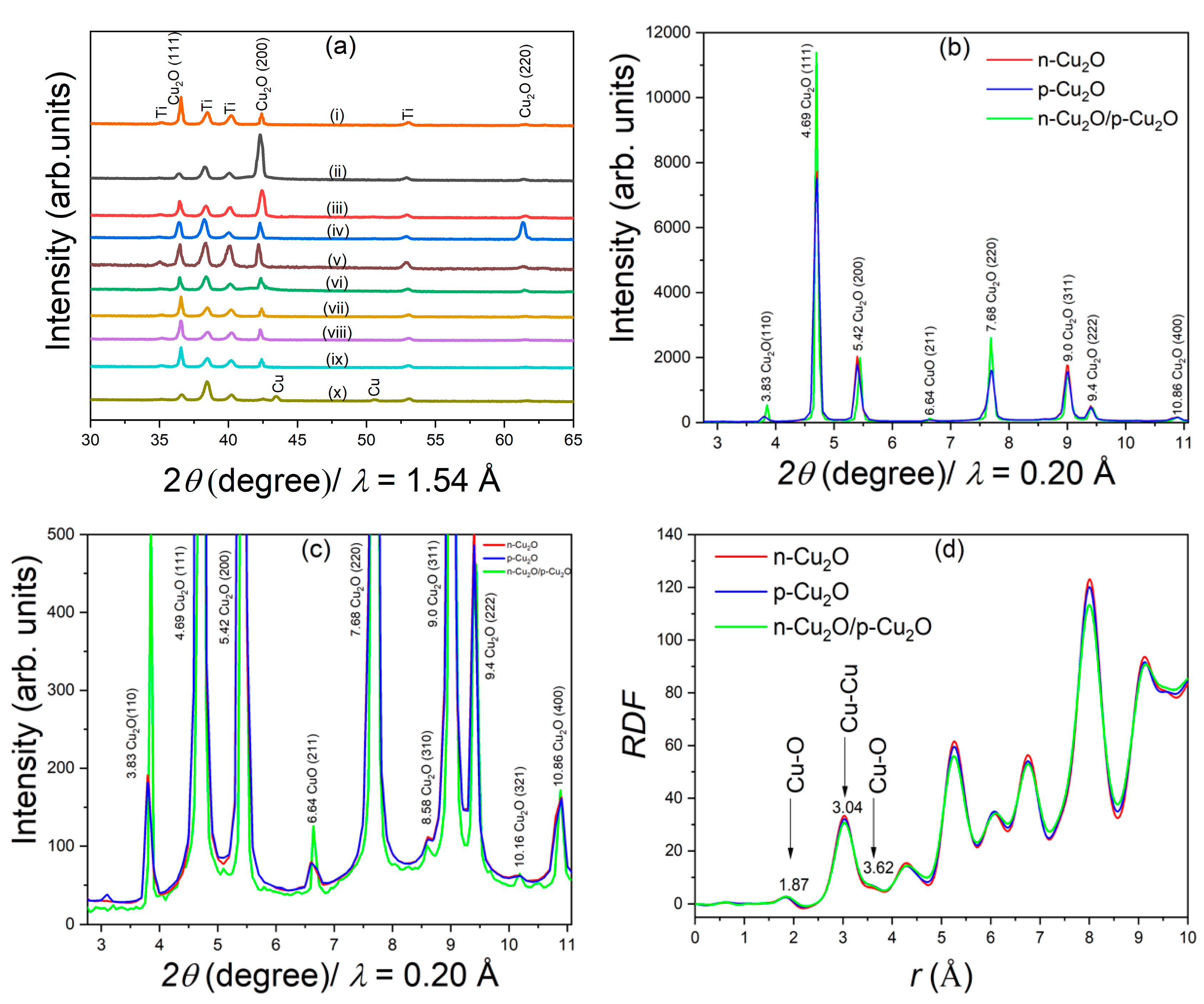
Figure 1a shows the X-ray diffraction (XRD) patterns of
n-type and
p-type Cu
2O films. XRD spectrum of the
n-Cu
2O films (
Figure 1a) shows a stronger reflection from (111) planes of Cu
2O, with a peak located at 2θ~36.48° (111) along with peaks at 2θ values of 42.24° (200), and 61.16° (220), respectively. The calculated diffraction intensity ratio of the (111) peak to the (200) peak was ~4.1. For the
p-type films (
Figure 1b–d), XRD peaks can be observed at 2θ values of 36.48°, 42.24°, and 61.16° corresponding to reflections from (111), (200), and (220) planes of Cu
2O, respectively. Also when
p-type films were deposited at pH 13.5, additional diffraction peaks arising due to the formation of copper can be seen at 43.22° (111) and 50.12° (200), respectively.
Relative intensities of the observed diffraction peaks varied with the deposition bath pH.
Table 2 shows the variation of calculated diffraction intensity ratio of the (111) peak to the (200) peak for the
p-type films with the deposition bath pH. It clearly shows that the preferred orientation of p-Cu
2O gradually transited from (200) to (111), giving a ratio of 4.15 at pH 12.5. Therefore, it can be seen that the maximum open-circuit voltage corresponded to the situation where the (111) to (200) diffraction peak intensity ratios were very nearly equal for the
n-type Cu
2O films deposited at pH 5.8 and
p-type Cu
2O films deposited at pH 12.5. It clearly shows that the maximum open-circuit voltage resulted when both the
n-type and
p-type Cu
2O films had similar crystalline orientations. It is possible that dissimilar crystalline orientations in the two films could introduce different interface states, which would offset the effect of the interfacial built-in electric field through the energy band bending. Therefore, we can conclude that the crystalline orientations are one of the key factors which contribute to the different open-circuit voltages shown in
Table 1.
The discussion below details the n-Cu2O/p-Cu2O homojunction fabricated by depositing n-type Cu2O films at pH 5.8 and p-type Cu2O films at pH 12.5, which were identified as the optimized deposition conditions. Compared to laboratory x-ray diffraction, with data of high signal-to-noise ratio, it is known that HEXRD can divulge more precise structural information of samples on the presence of species in the form of very thin layers or dilute quantities. Therefore, the n-type and p-type and p-n homojunction Cu2O thin films were subjected to HEXRD.
The HEXRD patterns of
n-type Cu
2O film (red),
p-type Cu
2O film (blue), and
p-n homojunction structures (green) grown with optimized deposition conditions are shown in
Figure 1b. HEXRD measurements exhibited a very low intense peak at 6.64° due to the (211) reflection of CuO, suggesting that the surface of Cu
2O interacted with air and formed CuO. It can be seen that both films showed a stronger (111) reflection at 4.69°. A similar distribution of intensities in the diffraction peaks, arising from the
p-type Cu
2O film deposited using a lactate bath at pH 12.5 and the
n-type Cu
2O film deposited using an acetate bath at pH 5.8, is indicative that films of both
n- and
p-type conductivities had similar orientations with the (111) to (200) peak intensity ratio of ~4. The sharper HEXRD peak profile arising from resulting
n-Cu
2O/
p-Cu
2O homojunction sample is indicative that it was made of good quality Cu
2O polycrystalline grains. It was later found that solar cell structures having
p-type and
n-type Cu
2O layers with similar orientations produced the highest open-circuit voltage, which can be attributed to the fact that similar orientations gave rise to an improved interface at the
p-Cu
2O/
n-Cu
2O junction.
Table 3 shows crystallographic parameters of the
n-Cu
2O (pH 5.8),
p-Cu
2O (pH 12.5), and
n-Cu
2O (pH 5.8)/
p-Cu
2O (pH 12.5) homojunction the HEXRD patterns were analyzed using the Rietveld refinement method [
30] for a pseudo-Voigt function. These lattice parameters and unit cell volumes are comparable to the previously reported theoretical and experimental values of Cu
2O (
a = 4.2696 Å) [
31].
Further, structural information was derived from HEXRD by mathematically converting the polarization-, absorption-, and background-corrected HEXRD data into a total structure factor,
S(
Q), and radial distribution function, (RDF), by Fourier transformation of
S(
Q) [
32].
Figure 1d shows the RDF spectra for the
n-type Cu
2O (red),
p-type Cu
2O (blue), and
n-Cu
2O (pH 5.8)/
p-Cu
2O (pH 12.5) (green), indicating that all three spectra showed similar RDF distributions with identical peak positions for
n-type Cu
2O,
p-type Cu
2O, and
n-Cu
2O/
p-Cu
2O homojunction. As indicated by the first and second peaks in
Figure 1d, the RDF peak analysis yielded 1.87 Å and 3.04 Å, respectively, for Cu-O and Cu-Cu correlations, agreeing with the Cu-O (1.849 Å) and Cu-Cu (3.012 Å) correlations of the standard Cu
2O powder [
31]. These values are also consistent with the lattice parameters reported above. In contrast, no peaks corresponding to Cu-O (1.95 Å) and Cu-Cu (2.9 Å) correlations for standard CuO powder [
31] or Cu-Cu (2.54 Å) correlations for Cu-foil were observable in the RDF pattern [
33].
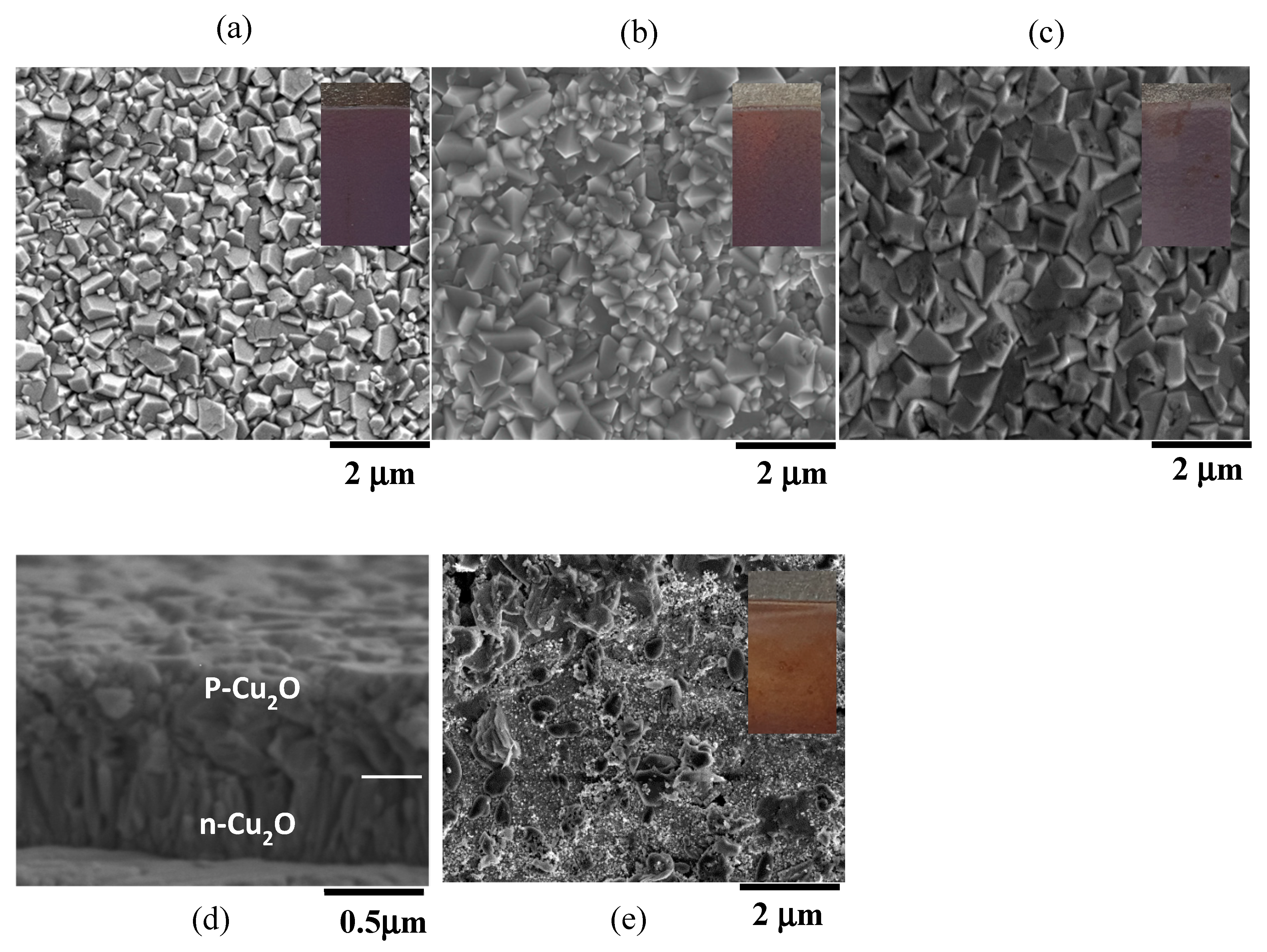
Figure 2a shows the top view of the SEM images of the
n-Cu
2O (pH 5.8) thin film deposited on Ti substrate with a uniform polycrystalline coverage consisting of grains with an average size of ~0.5 μm.
Figure 2b shows the SEM images of the
p-Cu
2O (pH 12.5) thin film deposited on Ti substrate with a uniform polycrystalline coverage consisting of grains of four-sided pyramids with a four-fold symmetry with an average size of ~ 0.1 μm. Good coverage was crucial for the use of these films for the
p-n device fabrication.
Figure 2c shows the surface morphology of the
p-Cu
2O/
n-Cu
2O homojunction structure. It is evident that the size of
p-Cu
2O crystals grown on
n-Cu
2O film was larger than that grown on bare Ti substrate (
Figure 2c), which was probably due to lower nucleation density and therefore the growth of larger crystals. After a layer of
p-Cu
2O was deposited on top of the
n-Cu
2O film, the surface morphology changed to polycrystalline grains of irregular shape. As shown in
Figure 2d, the thicknesses of
p-Cu
2O layer and
n-Cu
2O layer of the
p-n homojunction sample were ~0.5 μm.
Figure 2e shows the top view of the SEM images of the
p-Cu
2O film after the sulfur treatment, which resulted in a different surface morphology due to conversion of surface and grain boundaries to the other form.
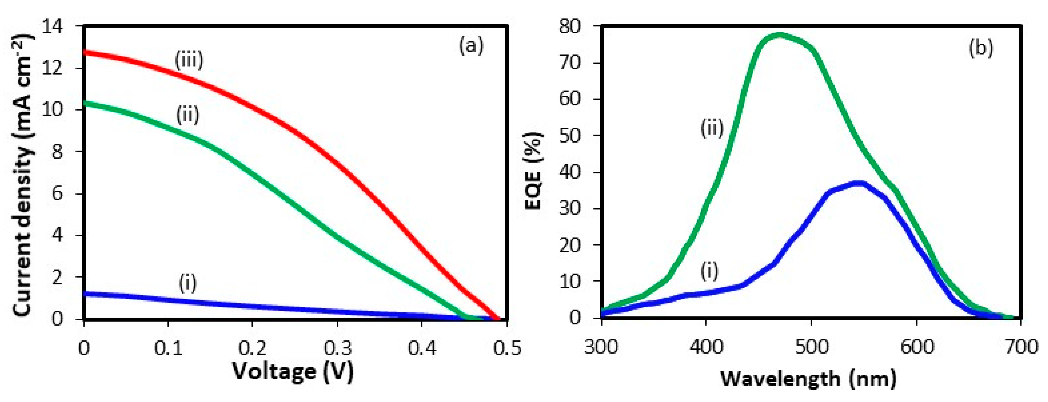
Figure 3a shows the current density-voltage characteristics of (i) untreated Ti/
n-Cu
2O/
p-Cu
2O/Au, (ii) sulfur-treated Ti/
n-Cu
2O/
p-Cu
2O/Au, and (iii) sulfur-treated and annealed Ti/
n-Cu
2O/
p-Cu
2O/Au solar cells device, respectively. The nonlinear J-V characteristics showed typical rectification behavior of a
p-n junction for the fabricated structures and confirmed the formation of homojunction. The untreated and unannealed Ti/
n-Cu
2O/
p-Cu
2O/Au solar cell structure produced an energy conversion efficiency of 0.26% with V
oc = 510 mV and J
sc = 1.23 mA cm
−2 under AM 1.5 illumination. It can be clearly seen that the sulfur treatment improved the J–V characteristics, and the unannealed and sulfur-treated Ti/
n-Cu
2O/
p-Cu
2O/Au solar cell structure produced an energy conversion efficiency of 1.94% with V
oc = 430 mV and J
sc = 10.2 mA cm
−2. Annealing of the sulfur-treated Ti/n-Cu
2O/p-Cu
2O/Au solar cell structure further improved the efficiency due to an improvement in the crystallinity and conductivity at an optimum annealing temperature and annealing time of 150 °C and 20 min, respectively, with an energy conversion efficiency of 2.64%, V
oc = 490 mV and J
sc = 12.8 mA cm
−2 under AM 1.5 illumination. This was a significant improvement compared to the efficiency of unpassivated and unannealed Ti/
n-Cu
2O/
p-Cu
2O/Au solar cell structures. One possible explanation for the improvement by sulfur is the formation of the Cu
2O/Cu
xS junction. However, the EQE spectra for the untreated and sulfur-treated cells presented in
Figure 3b showed that the onsets of EQE for both samples were around 640 nm, which corresponds to the band gap of Cu
2O.
Figure 3b also shows that the long wavelength response, which could be expected if the absorption in
p-type Cu
xS (band gap ~(1.2–1.5 eV)) layer occurs, was not present [
34]. Thus, the charge separation at the Cu
2O/Cu
xS interface became insignificant, making the junction ohmic. The untreated cell showed a maximum EQE of 35% near 550 nm unlike the sulfur-treated cell, which showed a maximum EQE of 80% around 470 nm. The maximum EQE of the sulfur-treated cell was nearly as twice as large as that of the untreated cell. The EQE of sulfur-treated cell was significantly increased at wavelengths below about 550 nm. The corresponding J
sc was enhanced from 1.23 mA cm
−2 to 10.2 mA cm
−2, as shown in
Figure 3a. This enhancement of short wavelength response suggests that, as the shorter wavelengths had short absorption depths than the longer wavelengths, the charge carriers were separated and collected more efficiently in the surface of the cell due to surface modification by sulfur. This could been caused by either absorption enhancement, decreased recombination, or both.
The surface elemental compositions of
p-Cu
2O/
n-Cu
2O homostructure sample and sulfur-treated
p-Cu
2O/
n-Cu
2O homostructure sample were further investigated by XPS to clearly examine the effect of sulfur.
Figure 4a shows survey X-ray photoelectron spectra of the (i) untreated
n-Cu
2O/
p-Cu
2O homostructure and (ii) sulfur-treated
n-Cu
2O/
p-Cu
2O homostructure. From the
p-Cu
2O/
n-Cu
2O homostructure sample, only peaks characteristic of Cu 2p, O 1s, and C 1s can be observed, and the sulfur-treated
p-Cu
2O/
n-Cu
2O homostructure sample has an additional signal that corresponds to S 2p. The weak peaks of C arose from adventitious hydrocarbon from the XPS instrument itself. All of the binding energies were calibrated by referencing C 1s peak (284.6 eV). The major Auger electrons peaks observed in XPS survey spectra included the O KLL and Cu LMM series, which were dependent on Mg Kα source [
35].
Figure 4b(i) shows the Cu 2p spectra obtained for the
p-Cu
2O/
n-Cu
2O homostructure. The XPS spectra in
Figure 4b(i) shows that the binding energies of the Cu 2p
1/2 and Cu 2p
3/2 were 952.5 eV and 932.6 eV, respectively, which are consistent with those observed at 952.5 eV and 932.18 eV for the Cu (I) oxidation state. Weak shake-up peaks of Cu (II) were also observed at 942.2 eV and 961.6 eV, respectively, indicating that the slight oxidation of some Cu (I) ions possibly presented on the surface and its vicinity to the CuO form [
36], which have been a product of Cu
2O surface oxidation when the sample was handled in air. Formation of the CuO phase in these Cu
2O films was a primary reason why these films exhibited an insulating behavior or poor electronic performance with extremely high resistivity [
37]. However, after sulfur treatment, the two satellite peaks in the Cu 2p XPS spectrum (indicated by circles in
Figure 4b which almost vanish and the binding energies of Cu 2p
3/2 and Cu 2p
1/2 which slightly shift to higher values (933.2 eV and 952.8 eV)) indicated the presence of CuS. The symmetrical nature of the two Cu 2p XPS peaks and the binding energy peaks observed in the S 2p spectrum at 162.1 eV and 163.2 eV (
Figure 4c), which were attributed to the S 2p
3/2 and S 2p
1/2 states, respectively, also confirmed the formation of CuS. The position of this S 2p peak was found to be consistent with the values reported by the authors of [
38]. From this result, it is more reasonable to confirm that the CuO of untreated samples was changed to CuS in the sulfur-treated samples and therefore reduced the resistivity. Therefore, the XPS study confirmed that the ammonium sulfide surface treatment caused the formation of very thin crystalline CuS films on the surface of the Cu
2O films. It has been reported that CuS shows a metal-like character, [
39,
40,
41] and it therefore make good ohmic contact, hence improving the carrier collection and enhancing the current density of sulfur-treated Ti/
n-Cu
2O/
p-Cu
2O/Au solar cell. As shown in
Figure 4d, the O1s core-level spectrum was broad, with a peak at 530.8 eV for untreated
n-Cu
2O/
p-Cu
2O homostructure and a peak at 531.2 eV for the sulfur-treated
n-Cu
2O/
p-Cu
2O homostructure which is consistent with the literature data of Cu
2O [
42]. Thus, the XPS results prove that the sulfur-treated sample was composed of Cu
2O.
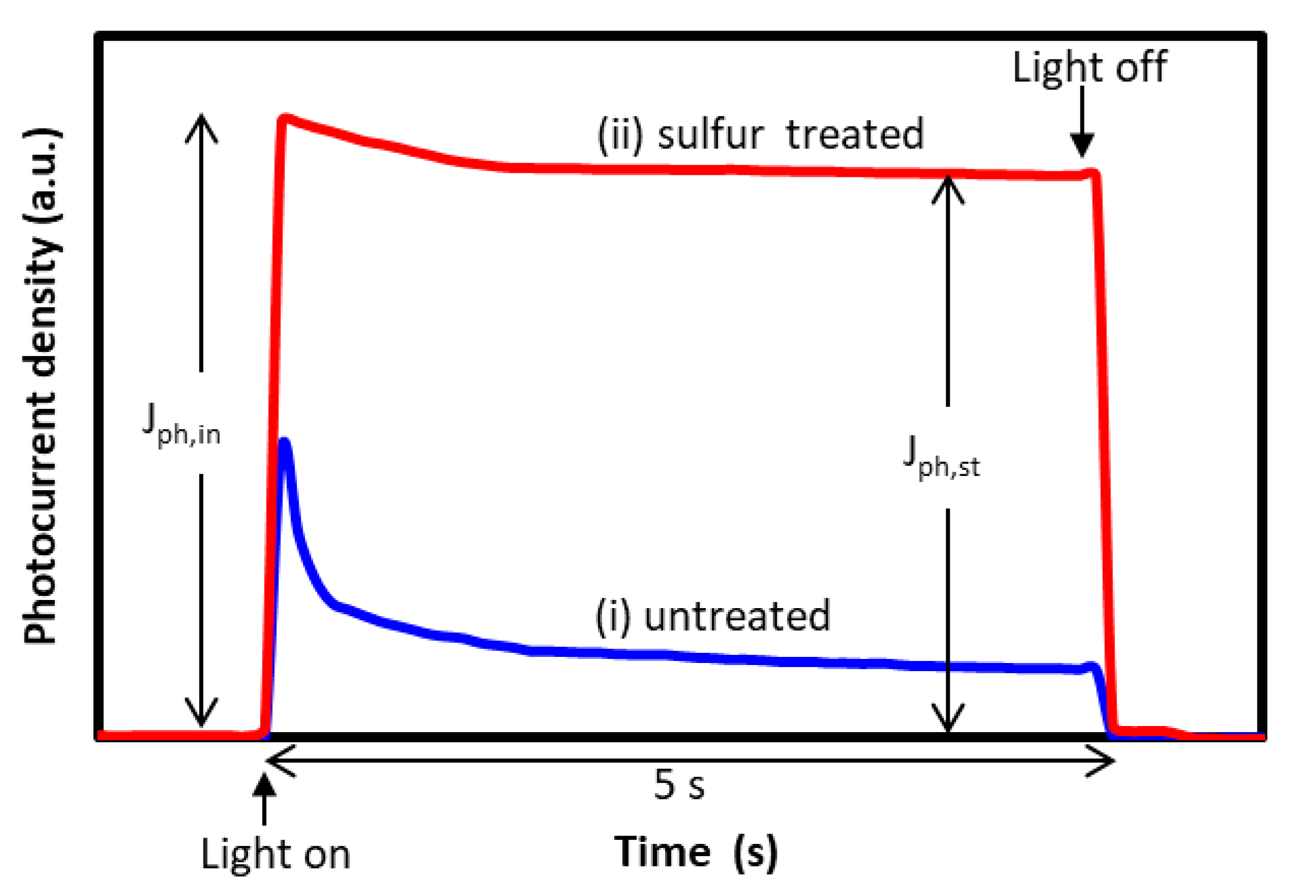
Salvador et al. [
43,
44] reported that the study of the photocurrent time transients is an interesting tool for the analysis of charge-transfer dynamics at the semiconductor/electrolyte interface. Therefore, in the present case and to assess the results shown in
Figure 5, the criteria described by Salvador et al. were taken into account, and the parameters shown in
Figure 5 were used as follows. An initial anodic photocurrent spike (j
Ph,in) appeared immediately after the application of the light pulse of intensity at time
t = 0. This current was associated with the separation of photogenerated electron-hole pairs at the depletion layer, and was therefore used as a measurement of the instantaneous flux of holes from the bulk toward the semiconductor/electrolyte interface when the illumination began
. Immediately, a slow decrease of the photocurrent as a function of time was observed, until a steady-state photocurrent value (
jPh,st) was reached for
. This steady-state photocurrent was linked to the equilibrium between the photocurrent maximum (
jPh,in) and the current associated with the recombination process (
jR) by the following equation:
where the “transient ratio”
jPh,st/
jPh,in becomes close to one, when the recombination rate tends toward zero:
In the case of the
n-Cu
2O/
p-Cu
2O homostructure, thin film electrode polarized at a 0.0 V (see
Figure 5) transient ratio value of 0.26 was obtained, which indicates a very high recombination rate of the photogenerated electron-hole pairs. On the other hand, when the sulfur treated
n-Cu
2O/
p-Cu
2O homostructure, a transient ratio value of 0.91 was obtained. This means that in the sulfur-treated samples with sulfur, the photogenerated electron–hole pairs exhibited a very low recombination rate. The improvements of initial anodic photocurrent spike and transition ratio clearly indicate that sulfur treatment improved the semiconducting properties of the
p-Cu
2O films, as the dangling bonds and surface CuO were both diminished.

 ,
, 


