Wideband Absorbing Plasmonic Structures via Profile Optimization Based on Genetic Algorithm
 Ruichao Zhu
  Jiafu Wang*
  Sai Sui* Yueyu Meng Tianshuo Qiu Yuxiang Jia Xiaofeng Wang Yajuan Han Mingde Feng Lin Zheng Shaobo Qu
- Department of Basic Sciences, Air Force Engineering University, Xi'an, China
Plasmonic structures that support the spoof surface plasmon polariton (SSPP) mode can be tailored to achieve strong absorption of electromagnetic (EM) waves. In particular, the profile of an absorbing plasmonic structure (APS) plays an important role in realizing its wideband absorption performance. In this paper, we propose a method of optimizing the longitudinal profile of APS based on Genetic Algorithm (GA), with the aim of obtaining high-efficiency wideband absorption of EM waves. The APS unit cell is composed of a longitudinal array of metallic strips, the length profile of which can be optimized to improve k-matching between free-space waves and SSPPs and meanwhile to customize absorption at each frequency within a wide band. Our investigation shows that non-linear variation of the strip lengths will make better k-matching and wideband absorption. As an example, a wideband APS is demonstrated using this method. The simulated and measured results show that the absorbance is higher than 90% in 10–30 GHz, which convincingly verifies the effectiveness of this method. This method provides an efficient approach to the design of radar absorbing structures and can also be extended to optimized design of other metamaterials.
Introduction
The electromagnetic wave transmission can be effectively suppressed by electromagnetic absorbers, which is why they can be widely applied in radar stealth techniques [1–3], electromagnetic protection [4, 5], and wireless transmission [6]. Metamaterials composed of artificially engineered subwavelength inclusions exhibit novel properties that cannot be found in nature or difficult to achieve [7, 8]. A significant breakthrough has been made for wave absorption thanks to the rapid development of electromagnetic metamaterials [9, 10]. Originated from optics, Surface Plasmon Polariton (SPP) is a transmission mode that is generated by the tight coupling between the electromagnetic (EM) wave and surface electron [11, 12]. On this basis, Pendry first proposed Spoof Surface Plasmon Polariton (SSPP) in earlier researches [13]. Exhibiting similar properties to Surface Plasmon Polariton (SPP) in optics, SSPP is an electromagnetic mode excited by artificial electromagnetic medium or structure in the microwave band [14, 15]. Subsequently, the SSPP of Transverse Magnetic(TM) and Transverse Electric(TE) were obtained by metamaterial [16, 17]. With the development of researches, the properties in the local field enhancement, strong dispersion and deep subwavelength characteristics of SSPP are widely applied in microwave absorbing, stealth and dispersion engineering [18–20]. Additionally, SSPP as absorbing metamaterial has also been applied in terahertz and infrared stealth [21, 22]. Therefore, SSPP has been extensively used as absorbing metamaterials by a lot of researchers.
It is worth noting that a longitudinal array of metallic strips overlapping with periodic arrangement can be combined with adjacent absorption peaks into a continuous adsorption peak [23, 24]. As metal strips increase, absorption bandwidth increases and metamaterials get thicker. Hence, a number of methods for reducing thickness of metamaterials were proposed such as introducing meandered strip structure, increasing high duty ratio of metal strips and loading other absorbing materials [25–28]. The SSPP performance can be affected by adjusting and controlling the length of horizontal metallic strip affects the impedance matching of electromagnetic wave, so its adjustment and control will also affect the SSPP performance, which, therefore can be improved by optimizing the longitudinal profile of strips. The conventional optimization algorithm includes heuristic algorithms such as Genetic Algorithm (GA) and Particle Swarm Optimization (PSO) [29–31], all of which has been widely applied in designing metamaterial and especially metasurface. The topology optimization in metasurface is currently restricted to the horizontal two-dimensional (2D) surface [32, 33]. However, optimization algorithm can also be expanded in vertical space. Therefore, we discuss the longitudinal profile of the Absorbing Plasmonic Structure (APS) and propose an optimization scheme adapted to the longitudinal profile's structure.
In this paper, we proposed the method that using GA to optimize the longitudinal profile of APS. This process is shown in Figure 1. The length of the horizontal metal strips in a specified thickness is simplified to a cubic function in the longitudinal direction. The coefficient matrix of polynomials was then regarded as the parameters to be optimized. The corresponding structural model can be built according to different curve functions. And then the mapping between the coefficient matrix and structure is established. Thus, the digital analysis of APS is realized. A large number of random samples were cross-iterated and selected according to the rules of GA. After optimization, the optimal coefficient matrix is obtained, the optimal structure is established, and the wideband absorber is realized. And finally, the wideband absorption with an efficiency of more than 90% in the frequency range of 10–30 GHz at the specified thickness was optimized. More importantly, when the objective function of GA is modified, the algorithm can also be applied to phase gradient design, dispersion engineering and other fields.
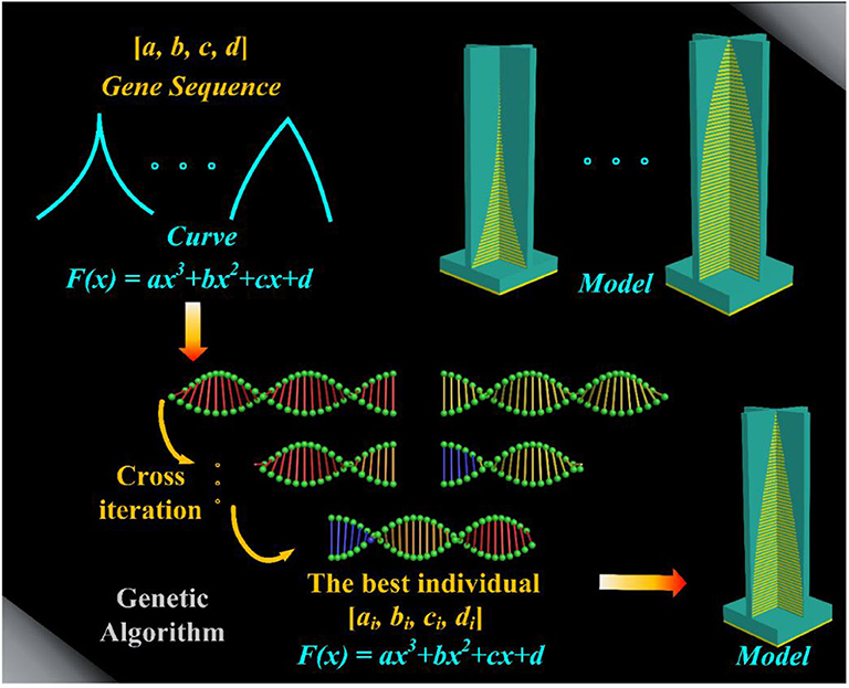
Figure 1. Schematic diagram of this work.
Absorber Design and Optimization Strategy
Design of Absorber
The APS with straight strips is designed as shown in Figure 2A, in which structural parameters are listed as follows: the height of vertical substrate h = 25.0 mm and the thickness d2 = 1.0 mm; the periodic distance of parallel straight strips s =0.4 mm and the width of strips w = 0.2 mm; the thickness of horizontal substrate d1 = 2.0 mm, the metal is copper with an electric conductivity of 5.8 × 10⁷ S/m and a thickness of t = 0.017 mm; the periodical length of absorber unit u = 10.0 mm. These parameters can be obtained in previous work [14, 34, 35]. The parallel straight copper strips with gradually varied length are bent, assembled and attached to the junction of dielectric substrates. The parallel straight strips lead electromagnetic(EM) waves from free space into absorber and form a standing wave between strips. In order to increase the loss of EM wave, a commercial dielectric substrate FR4 with a dielectric constant εr = 4.2 and a loss tangent tanδ = 0.025 is used as carrier of copper. The bottom of the absorber is consisted by a FR4 dielectric substrate backed with a copper reflector. The complete structure of the absorber is composed of design units, as shown in Figure 2B.
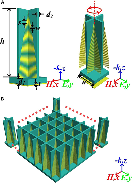
Figure 2. Schematic of straight-strip-shaped APS. (A) The design of absorber unit and (B) the complete absorber is consisted of absorber units.
Profile Optimization and Analysis
According to some researches, the longer length of the strip, the better it matches the low-frequency EM wave, and vice versa [13, 34, 36]. Based on the theory of APS, the impedance matching between the wave vector and absorber can be affected by the length of strip. Therefore, APS profile can be optimized for better wave absorption. The gradually varying external edges of these parallel straight strips can be regarded as some discrete points in a continuous curve. Because the structure is highly symmetrical, only one eighth of the structure needs to be designed. The value range of external edges of these parallel straight strips can be expressed as: x-axis in [0.5], y-axis in [0.25]. Within this range, a cubic function can fit arbitrary gradually changed curve. Thus, the optimization of parallel straight strips is transformed to the profile curve optimization of strip's external edge which is set as a cubic function as follows:
Where [a, b, c, d] is the coefficient matrix of the function f(x), and f(x) represents the curve of the longitudinal profile of APS. The curvilinear function f(x) affects the length of strip, as shown in Figure 3.
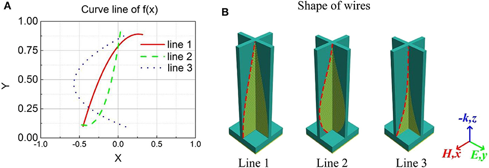
Figure 3. Curve and shape of strips. (A) Different curves generated by function f(x) and (B) the corresponding structure of SSPPs.
As shown in Figure 3, a variety of curves are generated by the cubic function f(x) with different coefficients. The curves are normalized to a specified region of the dielectric substrate, and the external edges of parallel straight strips vary gradually based on the function line f(x). The profile of APSs was then modeled by the curves in Figure 3A and the corresponding structure in Figure 3B. Therefore, the absorption effect of the parallel straight strips will be affected if the coefficient matrix [a, b, c, d] is adjusted. Hence, the optimization objective can be illustrated as Equation (2):
Where ΔFi is the continuous bandwidth in the desired frequency range [fmin fmax], which is 10–30 GHz in this paper. If the absorbance is >90%, the current frequency satisfies the requirements. The optimization objective is to achieve the absorbance that is >90% under normal incidence.
Equation (2) reveals that the wider the absorbing bandwidth, the less the fitness function value is. The optimization process is based on MATLAB-CST co-simulation and MATLAB optimization toolbox is applied as GA optimizer. The optimization process and result are shown in Figure 4.
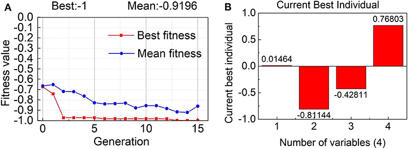
Figure 4. GA optimization. (A) The process of GA optimization and (B) the current best individual.
The results of the absorber optimized by GA were obtained by comprehensive simulation after 15 iterative evolutions, as shown in Figure 4. According to Equation (2), we can calculate the ratio of the current absorbing bandwidth in the total bandwidth. Figure 4A shows the process of GA optimization, the red line represents the variation of best fitness and the blue line represents the variation of mean fitness. The fitness is the value of function calculated by Equation (2). The best fitness is the optimal individual in the current generation. The mean fitness is the mean of all individuals in the current generation. According to the mean fitness, it can be seen intuitively that the population generated by GA is in a downward trend. Meanwhile, the best fitness also keeps a downward trend and gradually approaches the optimal value. The optimized wideband absorber is illustrated in Figure 4A, in which the best fitness value is −1, indicating that the best individual has been obtained. The coefficient matrix [a, b, c, d] of the current best individual is shown in Figure 4B. According to the optimization and simulation result, the best fitness is −1, implying that the absorber can achieve more than 90% of the absorbance in the frequency range of 10–30 GHz. The current best individual is [0.01464, −0.81144, −0.42811, 0.76803], therefore, the best curve function is f(x) = 0.01464*x3−0.81144*x2−0.42811*x + 0.76803. The parallel straight strips vary gradually based on above curve function and achieve better absorbing performance.
The parallel straight strips can be modified by the best line function, and the APS can be then modeled, as shown in Figure 5A. In order to verify the performance of the optimized APS, full-wave EM simulations were carried out using the time-domain solver in CST Microwave Studio. The simulation setups are as follows. The APS lies on XOY plane and the X-polarized waves are normally incident from the -Z direction. Remarkably, the structural unit is completely symmetric in the X and Y directions. In order to simulate an infinite continuous array while improving computing speed, the boundary conditions are introduced as follows: The X boundary condition is set to electric (Et = 0), the Y boundary condition is set to magnetic (Ht = 0). The Z boundary condition is set to open (add space). According to the simulation result in Figure 5B, the S11 is >10 dB in 10–30 GHz, implying that the absorbance is >90% in the work band. To understand the physical principle better, the distributions of surface current and power loss of the optimized model under different absorption frequencies are depicted in Figures 5C,D. It can be concluded that the different lengths of parallel straight strips produce resonance of different frequencies. Hence, the distribution of power loss is similar to that of surface current. The SSPPs transform EM waves in free space into surface waves and form standing waves, and the energy of EM wave is absorbed through a loss dielectric substrate. The resonance frequency is highly correlated to the length of parallel straight strips. Hence, the superposition of multiple resonant frequencies is achieved through the gradually varying strips, and then the wideband absorbing is achieved.
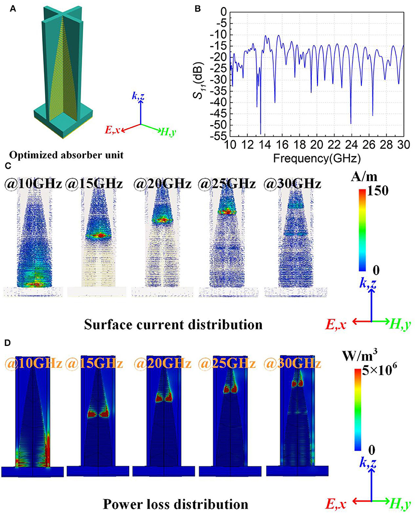
Figure 5. Electromagnetic response of the APS. (A) The model of optimized APS, (B) the simulation result of this model, (C) surface current distributions of the parallel straight strips in 10, 15, 20, 25, and 30 GHz, and (D) power loss distributions of the parallel straight strips in 10, 15, 20, 25, and 30 GHz.
The optimized absorber is theoretically analyzed to explore the causes of this model. In fact, the parallel straight strips can be equivalent to dipole [34]. The straight strips produce Lorentz resonance under the effect of the electromagnetic field. The upper boundary of the linear region is the cut-off frequency of the metal bar. With the increased frequency, the dispersion curves will gradually drift away from the light line and then get cut-off at certain frequencies. When the frequency is infinitely close to the cut-off, the maximum value of k-vector will produce the strongly localized surface wave, and the strongly localized surface wave always equipped with electric field enhancement, which makes the highly effective absorption close to the cutoff frequency [25].
CST Microwave Studio eigenmode solver is used to solve the dispersion relations for the electric dipole model with all the boundaries being set to period. Figure 6A illustrates the different lengths of strips corresponding to dispersion curves in the first Brillouin region. In order to further obtain the relations between strip length and cut-off frequency, their relations diagram shown in Figure 6B indicates that the length of strip l and frequency is non-linear. Long strip has a better match with high frequency, while short strip has a better match with low frequency. Therefore, if strip of corresponding length is matched with it in the appropriate frequency interval, the wideband matching effect can be obtained. When multiple electric dipoles are cascaded, the gradient structure of the parallel straight strips can facilitate the matching of the wave vector of SSPP and wave in free space and improve the coupling efficiency. As shown in Figure 6, the variation between strip length and cut-off frequency is non-linear. The APS can achieve a better absorbing performance because the profiles of parallel straight strips are also non-linear.
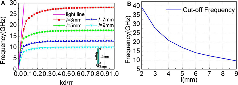
Figure 6. Dispersion diagram and cut-off frequency. (A) The dispersion diagram of the equivalent electric dipole of a short metallic strip patterned on a dielectric substrate and (B) the fitting curve between the unit length and frequency.
Experiment and Verification
In order to further verify the model, we fabricated a prototype of the optimized APS using conventional Printed Circuit Board (PCB) techniques. The photograph of the fabricated APS prototype is shown in Figure 7A. The size of APS array is 300 × 300 mm including 900 absorber units. Figure 7B illustrates the experiment measuring systems. The measurements were carried out in a microwave anechoic chamber based on a network analyzer (Agilent E8363B) with three pairs of broadband antenna horns with the frequency bands of 10–12 GHz, 12–18 GHz and 18–30 GHz. The measured results and simulated absorption spectra are shown in Figure 7C. It can be concluded from the measured results that all the test results are < -10 dB. However, some test results are not consistent, especially in the low frequency range. And the positions of the peaks and dips do not coincident at all, which is due to the error of machining and testing. As shown in Figure 7A, the APS is consisted by some components and the splicing of the modules results in poor electrical connectivity of the parallel straight strips at some intermediate junctions. However, the measured results are basically consistent with the simulation results. Additionally, the experience results demonstrate a better absorbing performance in the work band, thus proving that our method is effective.
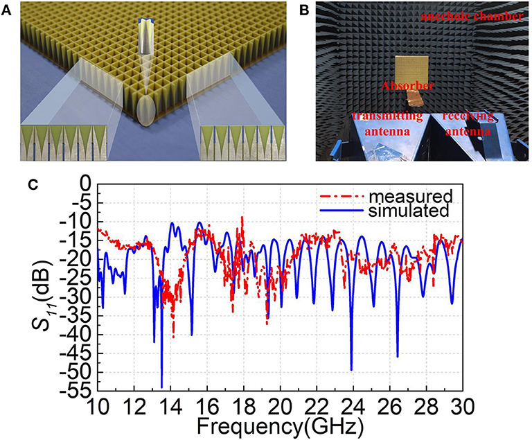
Figure 7. Measurement and results. (A) The photograph of the fabricated APS prototype, (B) the experiment measuring systems, and (C) the measured and simulated results of this APS.
Conclusion and Perspectives
In summary, we proposed a wideband absorber based on GA to achieve a better absorbing performance in the work band. The profile of parallel straight strips is regarded as a cubic function and the curve function is optimized by GA. Subsequently, the APS is optimized by GA with 15 generations, and then a best absorber is simulated, fabricated and measured. All the tested results are < -10 dB in the work band, thus proving that this method is effective. What's more, by analyzing the relation between the cut-off frequency and the length of parallel straight strip, we concluded that the non-linearly varying parallel straight strips can be better matched with wave vector. More importantly, this paper provides an idea for optimizing non-planar structure and a method to improve the performance in the specified thickness. And this method has a wide application prospect in electromagnetic protection and metamaterial design.
Data Availability Statement
The original contributions presented in the study are included in the article/supplementary material, further inquiries can be directed to the corresponding author/s.
Author Contributions
JW, SS, and SQ were the leaders of the work. RZ and TQ were responsible for the main of experiment and paper writing. YM, YJ, XW, and YH assisted in the experiment. MF and LZ were responsible for single step of the fabrication. All authors contributed to the article and approved the submitted version.
Funding
The authors are grateful to the support from the National Natural Science Foundation of China under Grant Nos. 61971435, 61971437, 61901508, 61671466, and 61671467, the Graduate Scientific Research Foundation of Department of Basic Sciences, the National Key Research and Development Program of China (Grant No.: SQ2017YFA0700201).
Conflict of Interest
The authors declare that the research was conducted in the absence of any commercial or financial relationships that could be construed as a potential conflict of interest.
References
1. Zhong S, Jiang W, Xu P, Liu T, Huang J, Ma Y. A radar-infrared bi-stealth structure based on metasurfaces. Appl Phys Lett. (2017) 110:6–11. doi: 10.1063/1.4975781
2. Iwaszczuk K, Strikwerda AC, Fan K, Zhang X, Averitt RD, Jepsen PU. Flexible metamaterial absorbers for stealth applications at terahertz frequencies. Opt Express. (2012) 20:635. doi: 10.1364/oe.20.000635
3. Yang Y, Yoke Leng L, Wang N, Ma Y, Ong CK. Electromagnetic field attractor made of gradient index metamaterials. J Opt Soc Am A. (2012) 29:473. doi: 10.1364/josaa.29.000473
4. Fan C, Tian Y, Ren P, Jia W. Realization of THz dual-band absorber with periodic cross-shaped graphene metamaterials. Chinese Phys B. (2019) 28:076105. doi: 10.1088/1674-1056/28/7/076105
5. Albano M, Micheli D, Gradoni G, Morles RB, Marchetti M, Moglie F, et al. Electromagnetic shielding of thermal protection system for hypersonic vehicles. Acta Astronaut. (2013) 87:30–9. doi: 10.1016/j.actaastro.2013.02.003
6. Wang B, Teo KH, Nishino T, Yerazunis W, Barnwell J, Zhang J. Experiments on wireless power transfer with metamaterials. Appl Phys Lett. (2011) 98:254101. doi: 10.1063/1.3601927
7. Zhang S, Genov DA, Wang Y, Liu M, Zhang X. Plasmon-induced transparency in metamaterials. Phys Rev Lett. (2008) 101:1–4. doi: 10.1103/PhysRevLett.101.047401
8. Boltasseva A, Atwater HA. Low-loss plasmonic metamaterials. Science. (2011) 331:290–1. doi: 10.1126/science.1198258
9. Landy NI, Sajuyigbe S, Mock JJ, Smith DR, Padilla WJ. Perfect metamaterial absorber. Phys Rev Lett. (2008) 100:1–4. doi: 10.1103/PhysRevLett.100.207402
10. Egorov V, Eitan M, Scheuer J. Genetically optimized all-dielectric metasurfaces. Opt Express. (2017) 25:2583. doi: 10.1364/oe.25.002583
11. Maier SA. Gain-assisted propagation of electromagnetic energy in subwavelength surface plasmon polariton gap waveguides. Opt Commun. (2006) 258:295–99. doi: 10.1016/j.optcom.2005.07.064
12. Lim SH, Mar W, Matheu P, Derkacs D, Yu ET. Photocurrent spectroscopy of optical absorption enhancement in silicon photodiodes via scattering from surface plasmon polaritons in gold nanoparticles. J Appl Phys. (2007) 101:2733649. doi: 10.1063/1.2733649
13. Pendry JB, Martín-Moreno L, Garcia-Vidal FJ. Mimicking surface plasmons with structured surfaces. Science. (2004) 305:847–8. doi: 10.1126/science.1098999
14. Yang J, Wang J, Feng M, Li Y, Wang X, Zhou X, et al. Achromatic flat focusing lens based on dispersion engineering of spoof surface plasmon polaritons. Appl Phys Lett. (2017) 110:1–6. doi: 10.1063/1.4983831
15. Ding F, Cui Y, Ge X, Jin Y, He S. Ultra-broadband microwave metamaterial absorber. Appl Phys Lett. (2012) 100:2010–4. doi: 10.1063/1.3692178
16. Lockyear MJ, Hibbins AP, Sambles JR. Microwave surface-plasmon-like modes on thin metamaterials. Phys Rev Lett. (2009) 102:073901 doi: 10.1103/PhysRevLett.102.073901
17. Liu N, Liu H, Zhu S, Giessen H. Stereo metamaterials. Nat Photonics. (2009) 3:157–62. doi: 10.1038/nphoton.2009.4
18. Shen Y, Zhang J, Meng Y, Wang Z, Pang Y, Wang J, et al. Merging absorption bands of plasmonic structures via dispersion engineering. Appl Phys Lett. (2018) 112:5040067. doi: 10.1063/1.5040067
19. Li SJ, Cao XY, Xu HX, Zhang Z, Zhou YL, Han JF, et al. Ultra-Wideband RCS reduction of metasurface antenna based on spoof surface plasmon polariton and transmission. Radio engineering. (2018) 27:386–93. doi: 10.13164/re.2018.0386
20. Meng Y, Ma H, Wang J, Li Y, Li Z, Qu S. BroadBand spoof surface plasmon polaritons coupler based on dispersion engineering of metamaterials. Appl Phys Lett. (2017) 111:1–6. doi: 10.1063/1.4995505
21. Zhu J, Ma Z, Sun W, Ding F, He Q, Zhou L, et al. Ultra-broadband terahertz metamaterial absorber. Appl Phys Lett. (2014) 105:4890521. doi: 10.1063/1.4890521
22. Li L, Xi R, Liu H, Lv Z. Broadband polarization-independent and low-profile optically transparent metamaterial absorber. Appl Phys Express. (2018) 11:052001. doi: 10.7567/APEX.11.052001
23. Cui Y, Fung KH, Xu J, Ma H, Jin Y, He S, et al. Ultrabroadband light absorption by a sawtooth anisotropic metamaterial slab. Nano Lett. (2012) 12:1443–7. doi: 10.1021/nl204118h
24. Fu JH, Wu Q, Zhang SQ, Zhang K, Meng FY. Design of multi-layers absorbers for low frequency applications. In: 2010 Asia-Pacific International Symposium on Electromagnetic Compatibility, Beijing (2010) 1660–1663. doi: 10.1109/APEMC.2010.5475478
25. Shen Y, Zhang J, Wang J, Pang Y, Ma H, Qu S. Multistage dispersion engineering in a three-dimensional plasmonic structure for outstanding broadband absorption. Opt Mater Express. (2019) 9:1539. doi: 10.1364/ome.9.001539
26. Wu C, Neuner B, Shvets G, John J, Milder A, Zollars B, et al. Large-area wide-angle spectrally selective plasmonic absorber. Phys Rev B Condens Matter Mater Phys. (2011) 84:1–7. doi: 10.1103/PhysRevB.84.075102
27. Cheng YZ, Gong RZ, Nie Y, Wang X. A wideband metamaterial absorber based on a magnetic resonator loaded with lumped resistors. Chinese Phys B. (2012) 21:127801. doi: 10.1088/1674-1056/21/12/127801
28. Shen Y, Zhang J, Wang W, Pang Y, Wang J, Ma H, et al. Overcoming the pixel-density limit in plasmonic absorbing structure for broadband absorption enhancement. IEEE Antennas Wirel Propag Lett. (2019) 18:674–78. doi: 10.1109/LAWP.2019.2900846
29. Jafar-Zanjani S, Inampudi S, Mosallaei H. Adaptive Genetic Algorithm for Optical Metasurfaces Design. Sci Rep. (2018) 8:1–16. doi: 10.1038/s41598-018-29275-z
30. Lalbakhsh A, Afzal MU, Esselle KP. Multiobjective particle swarm optimization to design a time-delay equalizer metasurface for an electromagnetic band-gap resonator antenna. IEEE Antennas Wirel Propag Lett. (2017) 16:912–5. doi: 10.1109/LAWP.2016.2614498
31. Jiang L, Zheng G, Shi L, Li X. Broad omnidirectional reflector design for optical telecommunications band using genetic algorithm. Japanese J Appl Physics, Part 1 Regul Pap Short Notes Rev Pap. (2008) 47:6333–6. doi: 10.1143/JJAP.47.6333
32. Zhang Q, Wan X, Liu S, Yin JY, Zhang L, Cui TJ. Shaping electromagnetic waves using software-automatically-designed metasurfaces. Sci Rep. (2017) 7:1–11. doi: 10.1038/s41598-017-03764-z
33. Yuan Q, Ma H, Sui S, Shen Y, Wang J, Feng M, et al. A broadband wide-angle synthetical absorber designed by topology optimization of resistance surface and metal wires. IEEE Access. (2019) 7:142675–81. doi: 10.1109/ACCESS.2019.2942495
34. Yang J, Wang J, Li Y, Pang Y, Meng Y, Cheng Q, Cui T, Qu S. 2D achromatic flat focusing lens based on dispersion engineering of spoof surface plasmon polaritons: broadband and profile-robust. J Phys D Appl Phys. (2018) 51:045108. doi: 10.1088/1361-6463/aaa11e
35. Wang X, Yan M, Fan Y, Fu X, Qu S, et al. Transmission-absorption integrated structure via dispersion engineering of spoof surface plasmon polariton and frequency selective surface. J Phys D Appl Phys. (2019). 53:085001. doi: 10.1088/1361-6463/ab56bd
Keywords: metamaterial, absorbing plasmonic structure, spoof surface plasmon polariton, wideband absorption, genetic algorithm
Citation: Zhu R, Wang J, Sui S, Meng Y, Qiu T, Jia Y, Wang X, Han Y, Feng M, Zheng L and Qu S (2020) Wideband Absorbing Plasmonic Structures via Profile Optimization Based on Genetic Algorithm. Front. Phys. 8:231. doi: 10.3389/fphy.2020.00231
Received: 05 May 2020; Accepted: 28 May 2020;
Published: 30 June 2020.
Edited by:
Zhi Hong, China Jiliang University, ChinaReviewed by:
Weiqiang Ding, Harbin Institute of Technology, ChinaIlia L. Rasskazov, University of Rochester, United States
Copyright © 2020 Zhu, Wang, Sui, Meng, Qiu, Jia, Wang, Han, Feng, Zheng and Qu. This is an open-access article distributed under the terms of the Creative Commons Attribution License (CC BY). The use, distribution or reproduction in other forums is permitted, provided the original author(s) and the copyright owner(s) are credited and that the original publication in this journal is cited, in accordance with accepted academic practice. No use, distribution or reproduction is permitted which does not comply with these terms.
*Correspondence: Jiafu Wang, wangjiafu1981@126.com; Sai Sui, suisai_mail@foxmail.com