Article

Correlated Time-0 and Hot-Carrier Stress Induced FinFET Parameter Variabilities: Modeling Approach

1
Institute for Microelectronics, TU Wien, 1040 Vienna, Austria
2
Imec, 3001 Leuven, Belgium
3
Department of Electrical Engineering (ESAT), KU Leuven, 3001 Leuven, Belgium
4
Ioffe Institute, 194021 St. Petersburg, Russia
*
Author to whom correspondence should be addressed.
Micromachines 2020, 11(7), 657; https://doi.org/10.3390/mi11070657
Submission received: 8 June 2020 / Revised: 27 June 2020 / Accepted: 29 June 2020 / Published: 30 June 2020

Abstract

:
We identify correlation between the drain currents in pristine n-channel FinFET transistors and changes in time-0 currents induced by hot-carrier stress. To achieve this goal, we employ our statistical simulation model for hot-carrier degradation (HCD), which considers the effect of random dopants (RDs) on HCD. For this analysis we generate a set of 200 device instantiations where each of them has its own unique configuration of RDs. For all “samples” in this ensemble we calculate time-0 currents (i.e., currents in undamaged FinFETs) and then degradation characteristics such as changes in the linear drain current and device lifetimes. The robust correlation analysis allows us to identify correlation between transistor lifetimes and drain currents in unstressed devices, which implies that FinFETs with initially higher currents degrade faster, i.e., have more prominent linear drain current changes and shorter lifetimes. Another important result is that although at stress conditions the distribution of drain currents becomes wider with stress time, in the operating regime drain current variability diminishes. Finally, we show that if random traps are also taken into account, all the obtained trends remain the same.

1. Introduction

One of the main problems plaguing performance of modern ultra-scaled field-effect transistors (FETs) is variability, which has multiple sources: random dopants (RDs) [1], perturbation in material properties [2,3], oxide thickness fluctuations [4,5], etc. This variability manifests itself already in pristine devices and therefore is named “time-0 variability”. In a very similar manner, build-up of defects during stress is a stochastic process and therefore degradation in ultra-scaled devices should be described statistically as time-dependent variability [6].
A link between these two types of variabilities has been a subject of previous studies. Investigations conducted by Kerber et al. [7,8] resulted in a correlation between distributions of the threshold voltage V th in unstressed devices and threshold voltage changes Δ V th induced by bias temperature instability (BTI). Quite to the contrary, Angot et al. [9] and Hussin et al. [10] did not reveal any correlation between time-0 V th values and their BTI-induced shifts Δ V th . The latter group has been very actively studying the correlation between time-0 and stress induced variabilities also in the context of self-heating [11] and random dopant induced percolation paths in FETs [12].
As for hot-carrier degradation (HCD), which has been repeatedly declared to be the most detrimental reliability concern in ultra-scaled FETs [13,14], although HC induced variability was a subject of experimental [15,16,17,18,19,20,21] and modeling [22,23,24,25,26,27,28] studies, to the best of our knowledge there is a limited number of publications devoted to correlation between time-0 and HC stress induced transistor parameter distributions [29,30,31], and no simulation studies of this correlation have been performed so far. Schlünder et al. [29] reported a strong correlation between parameters in the { V th ( t = 0 ) , Δ V th } and { I d ( t = 0 ) , Δ I d } tuples (here t is the stress time, while I d is the drain current). This study showed that devices with initially higher drain currents degrade faster and therefore have larger Δ I d values and shorter device lifetimes τ . A very similar trend was reported also by Ramey and co-authors [30], i.e., devices with initially higher V th values demonstrated slightly larger Δ V th changes. Finally, the work of Federspiel et al. [31] also reports correlation between time-0 threshold voltages and their HC induced drifts; the authors also identified correlation between changes of the threshold voltage and the drain current during HCD and this finding is consistent with the results from [30].
However, a physics-based modeling framework for HCD which can capture these experimental trends is still missing. In this work, we perform the first theoretical study of the correlation between time-0 values of the linear and saturation drain currents ( I d , lin ( 0 ) and I d , sat ( 0 ) , respectively) in n-channel FinFETs and relative drain current changes ( Δ I d , lin and Δ I d , sat ) induced by HC stress. For this we employ our approach to stochastic HCD modeling [23,25,26]. We consider the roles of impacts of random dopants and random traps on this correlation.

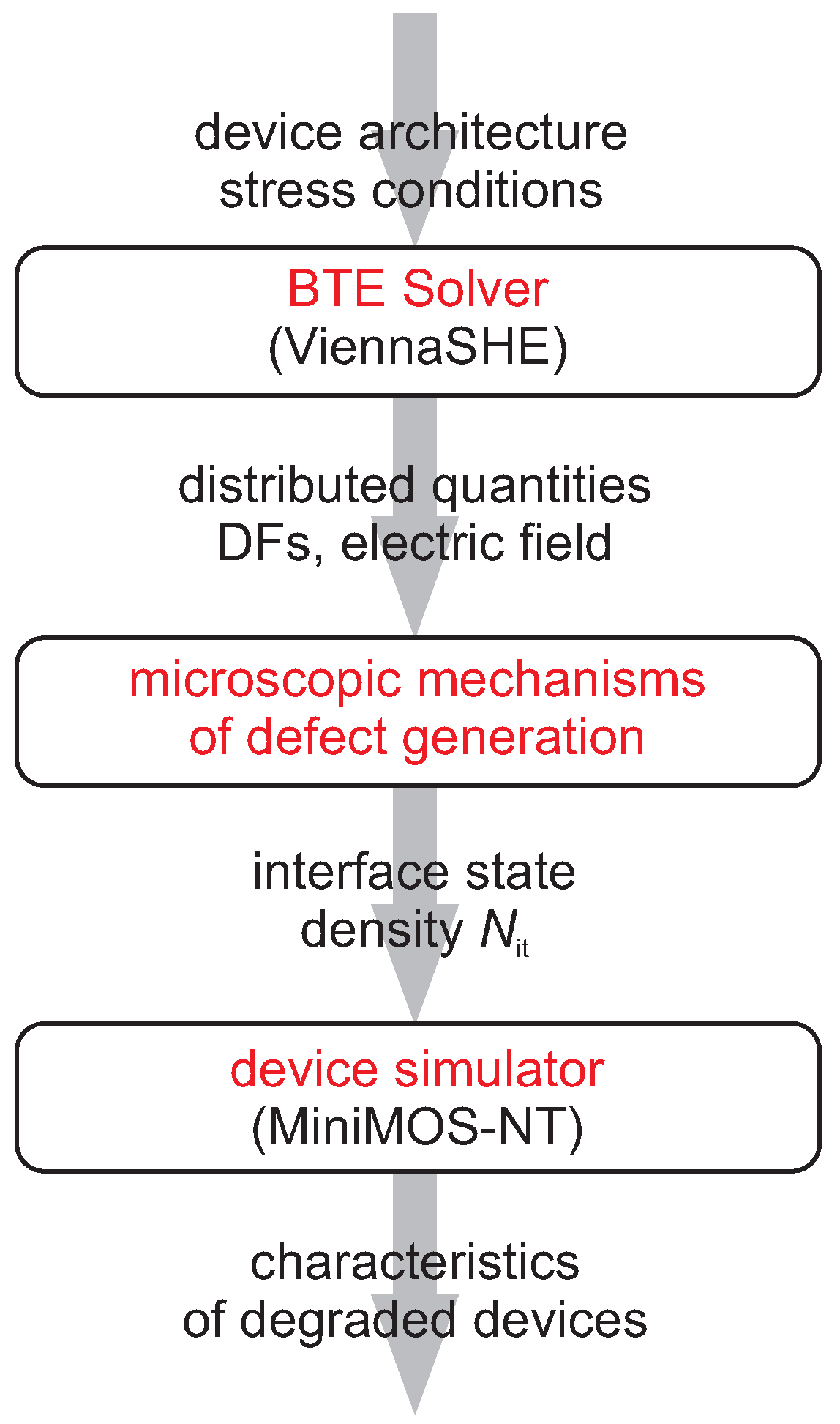
2. The Modeling Framework

The stochastic version of our HCD model (which is described in greater detail in [23,25]) is derived from the deterministic approach to HCD simulations validated against data acquired in devices of different types, which include planar FETs [32,33], power laterally-diffused metal-oxide semiconductor transistors [34,35], FinFETs [36] and nanowire FETs [37]. To accurately describe the complex physical picture behind HCD, this approach captures and links carrier transport, a microscopic description of defect generation rates, and modeling of the degraded devices, see Figure 1, which sketches the model structure.

2.1. Carrier Transport Modeling

For carrier transport modeling we use the deterministic solver of the Boltzmann transport equation (BTE) ViennaSHE [38,39,40,41], which is based on the spherical harmonics expansion of the carrier energy distribution function (DF). ViennaSHE incorporates the real band structure of Si and models the rates of different scattering mechanisms including impact ionization, surface scattering, ionized impurity scattering as well as electron-phonon and carrier-carrier interactions. The effect of traps generated by HCD was recently incorporated into ViennaSHE [42]. ViennaSHE solves the bipolar BTE for a particular device architecture and specified stress or operating conditions. Note that for obtaining the carrier DFs one can use another transport simulator, as for example a stochastic BTE solver based on the Monte Carlo method (in the first version of our HCD model [43,44] we used the simulator MONJU based on the Mote Carlo approach to the BTE solution [45]).

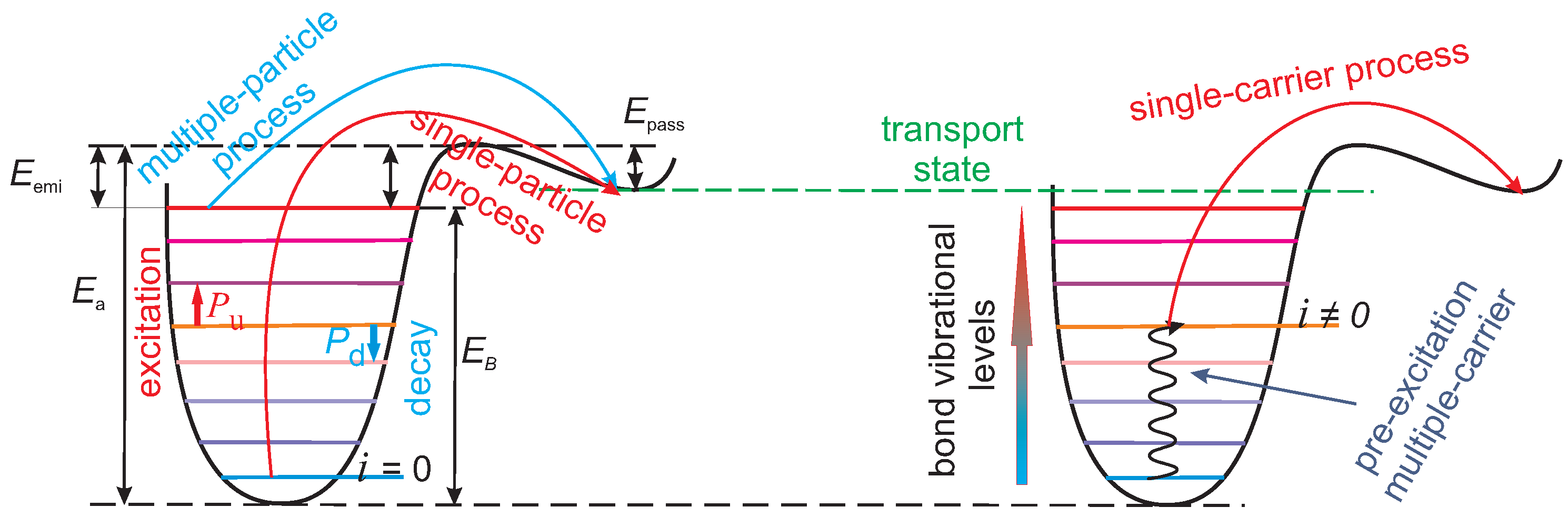
2.2. Defect Generation

The carrier energy DFs are then used to calculate the rates of single- and multiple-carrier mechanisms (SC- and MC-mechanisms) of Si-H bond breakage (Figure 2). Under stress conditions with high drain voltages carriers can be accelerated up to energies exceeding the bonding energy of the Si-H bond which is E a = 2 . 6 2 . 9 eV [46,47,48] and therefore they are able to trigger bond rupture in a single collision. This scenario is called “single-carrier mechanism” of bond dissociation and was dominant in high-voltage devices and/or old technology nodes [49,50,51]. Under lower drain voltages these highly energetical carriers have low concentrations and therefore the single-carrier mechanism has a negligibly low rate. However, several cold carriers can subsequently bombard the bond and induce its multiple vibrational excitation, which eventually results in a bond rupture event; this scenario is named “multiple-carrier mechanism” and has high rates in ultra-scaled devices [52,53,54,55]. One can say that the single-carrier mechanism is driven by hot carriers, while the multiple-carrier process is associated with cold carriers. This is the main reason why we need to know how carriers are distributed over energy and solve the BTE to obtain the carrier DFs. If a bond is pre-heated by several cold carriers to some excited by still bonded state (Figure 2, right panel) with an index i and the energetical position E i the bond-breakage energy is reduced by the value E i and is effectively equal to E a E i . Therefore, the probability of a single-carrier bond breakage event from this level i dramatically increases. Recently it was reported that in modern ultra-scaled devices the most probable path of bond dissociation is via a mixture of multiple- and single-carrier mechanisms of bond dissociation [33,56,57].
We model the Si-H bond within the truncated harmonic oscillator model, i.e., the bonding potential is parabolic and the eigenstates of the bond are equidistantly spaced with the distance between them being ω , see Figure 2. The dissociation reaction occurs via the stretching mode of the bond (another vibrational mode of the Si-H bond is the bending mode). This is because the bonding energy of this mode E a = 2.56 eV (Figure 2) corresponds to the bond-breakage energy measured during experiments of bond dissociation [48]; the corresponding parameter ω is equal to 0.25 eV. To model the rates of the SC- and MC-mechanisms we employ the formalism described in sufficient detail in [32,33,57,58]. The rates of both SC- and MC-mechanisms are determined by the carrier acceleration integral:
I SC | MC = E th f ( ε ) g ( ε ) σ SC | MC ( ε ) v ( ε ) d ε .
Here f ( ε ) is the carrier DF obtained with ViennaSHE, g ( ε ) the density-of-states of the corresponding carrier band, v ( ε ) the carrier group velocity and integration is performed over carrier energy ε . The Keldysh-like reaction cross section σ SC | MC ( ε ) for both processes is given by
σ SC | MC ( ε ) = σ 0 , SC | MC ( ε ε th ) / 1 eV p SC | MC ,
with the parameters p SC and p MC being equal to 11 and 1 for SC- and MC-processes, correspondingly [43,58]. For the MC-mechanism the threshold energy is equal to the distance between the oscillator levels ω , while for the SC-mechanism occurring form the ground state of the bond (Figure 2, left panel) we assume ε th = E a . The prefactors σ 0 , SC | MC are adjustable parameters of the model.
If the bond is preheated by several cold carriers (Figure 2, right panel) to a bonded state i the SC-mechanism rate reads
I SC , i ( E a ) = f ( ε ) g ( ε ) σ 0 ( ε E a + E i ) p it , SP v ( ε ) d ε
and the total bond rupture rate from this level is
R SC , i = w th exp E a E i ) / k B T L + I SC , i ,
where the first term is the rate of the thermal activation of the bond over the potential barrier between the level i and the transport mode (with the corresponding attempt rate w th ) and I SC , i is the SC-process rate.
To model the bond dissociation kinetic we employ the system of rate equations for each eigenstate (the last bonded state is labeled as N l , see Figure 2):
d n 0 d t = P d n 1 P u n 0 R a , 0 n 0 + R ˜ p , 0 N it 2 d n i d t = P d ( n i + 1 n i ) P u ( n i n i 1 ) R a , i n i + R ˜ p , i N it 2 d n N l d t = P u n N l 1 P d n N l R a , N l n N l + R ˜ p , N l N it 2 .
In these equations, n i is the level occupation number and the rates P u , P d correspond to bond excitation and deexcitation, N it is the concentration of interface traps and R ˜ p , i is the normalized passivation rate.
The rates of bond heating and cooling are
P u = ω e exp ω / k B T L + I MC , P d = ω e + I MC ,
with ω e being the vibrational frequency of the bond and which is equal to the reciprocal vibrational lifetime τ e (for the stretching mode this lifetime is equal to 1.5 ns at room temperature [59]) and the term I MC is the rate of the MC-process calculated by (1).
We solve the system (5) assuming the hierarchy of time scales, i.e., taking into account that bond heating and cooling processes have much shorter characteristic times than the bond rupture and passivation mechanisms. Within this approach the system reduces to a single differential equation:
d N it d t = N 0 N it R a N i t 2 R ˜ p ,
where N 0 is the concentration of electrically inactive Si-H bonds at the interface and R a is the cumulative bond breakage rate:
R a = 1 k i R a , i P u P d i ,
where summation is performed over all bonded levels and bond rupture rates are weighted with the corresponding occupation numbers
n i = 1 k P u P d i .
Here k is the prefactor which ensures normalization n i = 1 and is equal:
k = i P u P d i .
The passivation rate, which is determined as R ˜ p = i R ˜ p , i , can be simplified and modeled as a thermal activation over a single barrier E pass :
R p = ν p exp ( E pass / k B T L ) ,
where ν p is the attempt rate. As for the normalized rate entering (5) it is determined as R ˜ p = R p / N 0 . Following experimental papers [60,61,62] we use E pass = 1 . 5 eV.
The system of rate equations (5) simplified as (7) has an analytical solution:
N i t ( t ) = R a 2 / 4 + N 0 R a R ˜ p R ˜ p 1 f ˜ ( t ) 1 + f ˜ ( t ) R a 2 R ˜ p , f ˜ ( t ) = R a 2 / 4 + N 0 R a R ˜ p R a / 2 R a 2 / 4 + N 0 R a R ˜ p + R a / 2 exp 2 t R a 2 / 4 + N 0 R a R ˜ p .
Here the time dependencies of N it is determined by the component f ˜ ( t ) .
Due to the amorphous nature of SiO2 the bonding energy E a is a fluctuating quantity and in the model it is assumed to follow the normal distribution with the mean value E a = 2.56 eV [46] and a certain standard deviation σ E which depends on the particular technology node (an adjustable parameter of the model).

2.3. Modeling of the Degraded Devices

The interface traps generated during HC stress are amphoteric and can capture electrons and holes. Since the concentration N it varies with the coordinate along the Si / Si O 2 interface the corresponding charge incorporated into the transistor is also non-uniformly distributed. The impact of this charge on device performance is twofold: (1) charged traps locally perturb the device potential profile and (2) scatter carriers, thereby degrading the mobility.
To model these two aspects we use the device and circuit simulator MiniMOS-NT [63] which employs drift-diffusion and energy transport schemes as simplified approaches to the BTE solution. MiniMOS-NT also has a solver for the Poisson equation which captures the effect of interface traps on the device electrostatics. As for the reduction in the carrier mobility we use an empirical model [64,65]:
μ it = μ 0 1 + α it N it exp ( r / r ref ) ,
where μ 0 corresponds to the mobility of the pristine device, α it is the parameter which determines the magnitude of the impact of interface traps on the carrier mobility, r the distance from the carrier to the Si / Si O 2 interface, and r ref the characteristic length at which the carriers “feel” the interface charges. Strictly speaking, the quantities α it and r ref are adjustable parameters of the model, however during model validation/calibration these parameters are not the subject for optimization and we always use α it = 10 13 cm 2 and r ref = 1 nm.

2.4. Calibration of the Deterministic Model for HCD

We employ n-channel FinFETs with a gate length of 40 nm (the corresponding channel length is 28 nm), a high-k gate stack (containing SiO 2 and HfO 2 layers) with an EOT of ∼1.2 nm, and an operating voltage of V dd = 0.9 V. The FinFET geometry and dimensions such as the fin width and height are shown in Figure 3, left panel. To obtain the device architecture (including the doping profiles) we used the Sentaurus Process simulator [66], which was coupled to the device simulator MiniMOS-NT [63] in the GlobalTCADSolutions framework [67]. These two simulators were calibrated self-consistently by reproducing current-voltage characteristics of the pristine transistor; this is a very important step of the entire simulation framework because carrier energy distribution functions are very sensitive to variations in doping profiles.
These devices were stressed at the HCD worst-case conditions for short-channel devices for three different combinations of gate and drain voltages ( V gs , V ds ): V ds = 1.6 V, V gs = 1.7 V; V ds = 1.7 V, V gs = 1.8 V; and V ds = 1.8 V, V gs = 1.9 V. At each time step t, stress was interrupted to measure Δ I d , lin ( t ) changes ( I d , lin corresponds to V ds = 0.05 V and V gs = V dd ); the corresponding experimental Δ I d , lin ( t ) traces are summarized in Figure 4. It is noteworthy that we consider relative changes of the drain current, i.e., absolute changes of linear and saturation currents were normalized to the current values of the unstressed samples I d , lin ( 0 ) and I d , sat ( 0 ) (which are different for various “samples”), respectively. Further, unless stated otherwise, under “normalized changes” in the current we understand Δ I d , lin ( t ) = | I d , lin ( t ) I d , lin ( 0 ) | / I d , lin ( 0 ) and Δ I d , sat ( t ) = | I d , sat ( t ) I d , sat ( 0 ) | / I d , sat ( 0 ) . In some special cases we also employ normalization to the mean degradation values (e.g., Δ I d , lin ( t ) / Δ I d , lin ( t ) ). Let us also emphasize that typically drain currents decrease during HC stress, however, Δ I d , lin and Δ I d , sat values defined in the afore-described manner increase with time. Showing degradation chages in absolute values is commonly used for HCD characterization and modeling by many groups [56,68,69,70,71,72,73,74,75,76] because degradation traces presented in this form can be plotted on a log-log scale to enable empirical fitting. Figure 4 borrowed from our recent publication [36] demonstrates that our model can thoroughly represent experimental Δ I d , lin ( t ) traces for all three stress conditions.
Note finally that the model does not consider the impact of self-heating on HCD. Although we recently presented a simulation framework which models coupled hot-carrier degradation and self-heating in nanowire FETs [77], analysis of the impact of self-heating on HC induced variability is outside the scope of this paper.

2.5. The Stochastic Model for HCD

The device structure generated by Sentaurus Process with continuous doping profiles was used as a template to generate 200 instantiations with different configurations of discrete random dopants [23,25]. To achieve this goal, for each mesh cell of the initial device we multiplied the local doping concentration by the volume of this cell, thereby obtaining the mean value of the number of dopants contained in this cell. In each of these FinFET instantiations we consider the number of dopants in each cell as a stochastic variate and to generate 200 different realizations of this variate we use a Poisson random number generator with the mean value obtained from the device structure with continuous doping concentrations. This randomization procedure was applied to both donors and acceptors in all device segments including the source, drain, channel, source/drain extensions, etc.
Therefore, each of these 200 “samples” has its own unique configuration of RDs and, as a consequence, unique values of I d , lin ( 0 ) values, see Figure 3. For each of these instantiations we solved the Boltzmann transport equation, obtained carrier DFs, computed the corresponding interface state densities N it (Figure 3) and generated ensembles of Δ I d , lin ( t ) and Δ I d , sat ( t ) traces (note that I d , sat is measured at V gs = V ds = V dd ). In addition to the aforementioned stress conditions, we carried out all these simulations for lower biases of V gs = V ds = 1.0 V which are close to the operating voltage V dd .
The obtained continuous N it densities were also a subject for discretization/randomization [24,26]. In a similar manner as in the case of RDs we multiplied the local N it value by the cell area (a cell at the interface is two-dimensional though), thereby obtaining the mean number of traps which was then used in a Poisson randomizer to obtain the fluctuating number of interface traps in the cell. Special attention was paid that this randomization procedure does not result in a statistically scattered number of traps which is lower at the next stress time step as compared to the current step; in other words the discretized number of traps should be a non-reducing function of time.
To summarize, for each combination of stress voltages V ds , V gs we generated 200 different configurations of RDs and then each of them, in turn, has 200 different realizations of RTs. Therefore our ensemble contained 40,000 different structures with unique RD and RT configurations.
Based on the initial 200 instantiations with RDs we calculated ensembles of Δ I d , lin ( t ) and Δ I d , sat ( t ) traces and extracted corresponding device lifetimes. For this extraction, we used the criterion that device lifetime corresponds to stress time at which the normalized Δ I d , lin (or Δ I d , sat ) reaches a value of 0.1. In the case of 40,000 different configurations of RDs and RTs we modeled only Δ I d , lin and corresponding lifetimes.

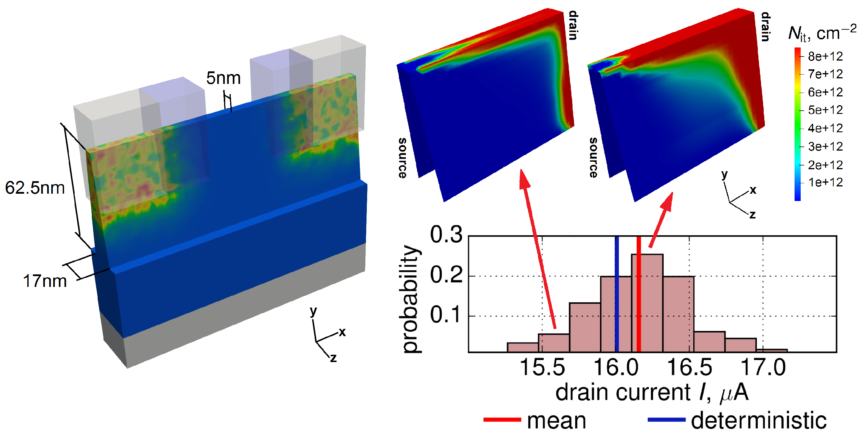
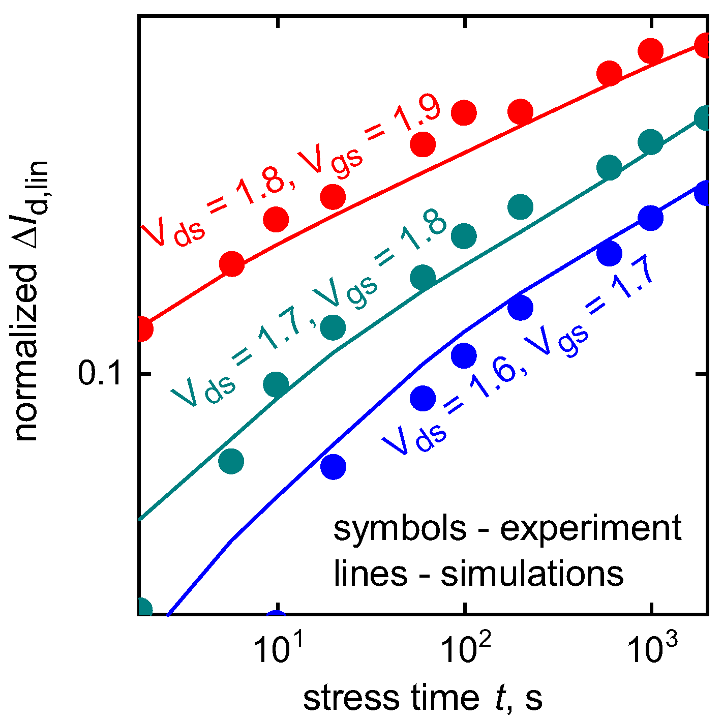
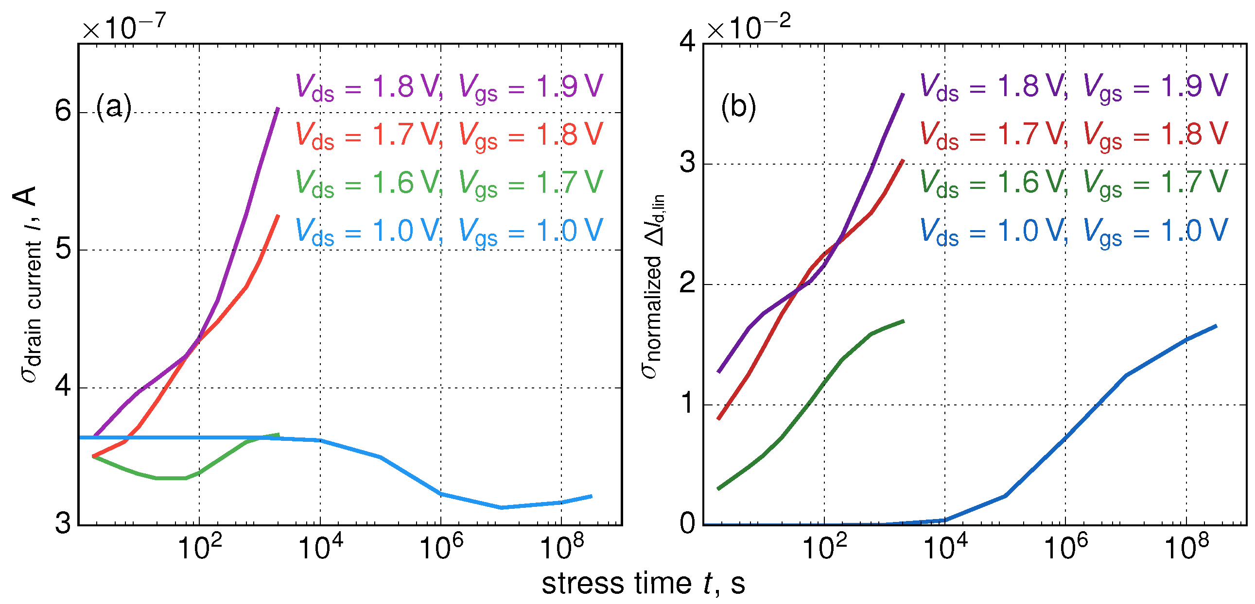
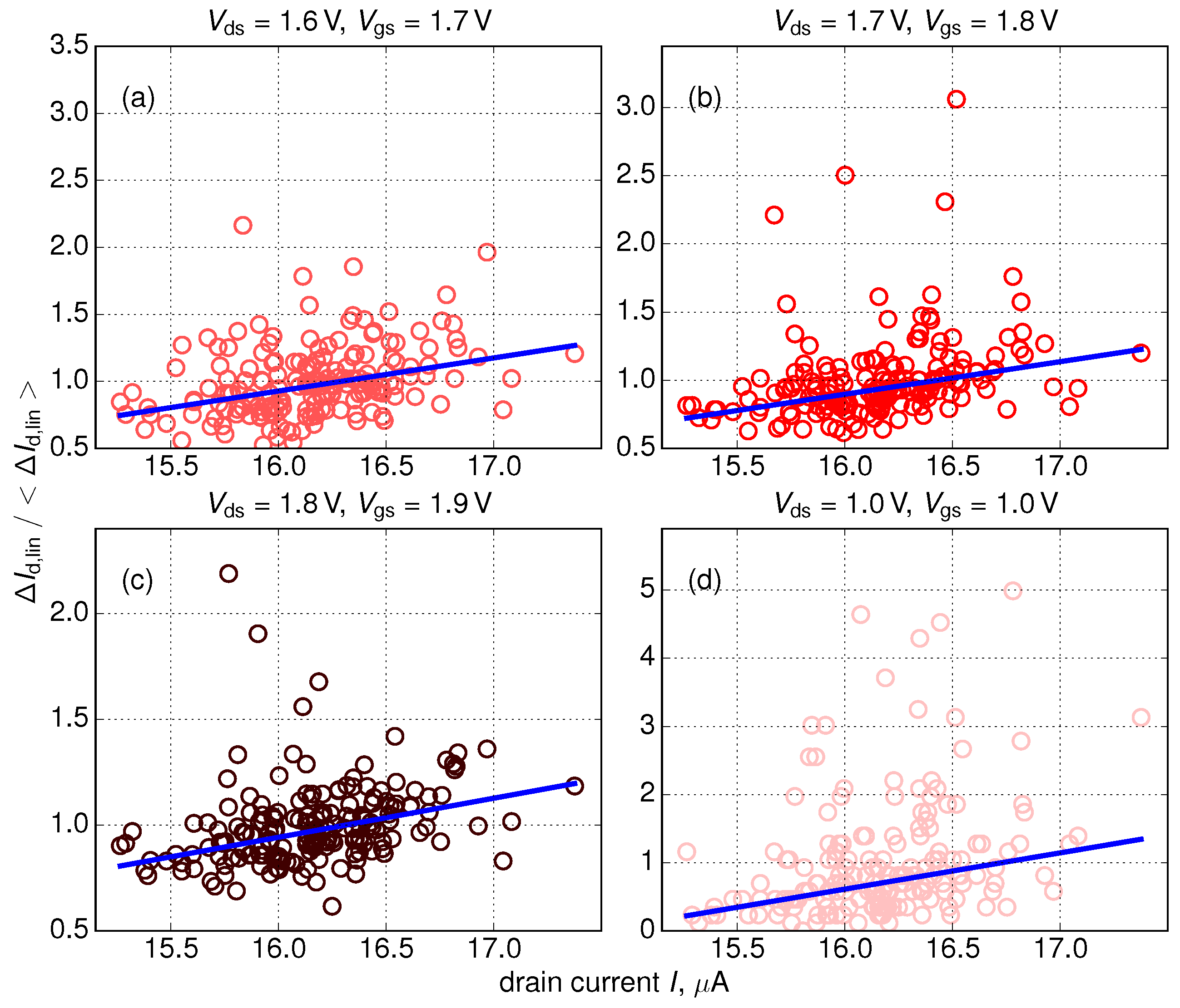
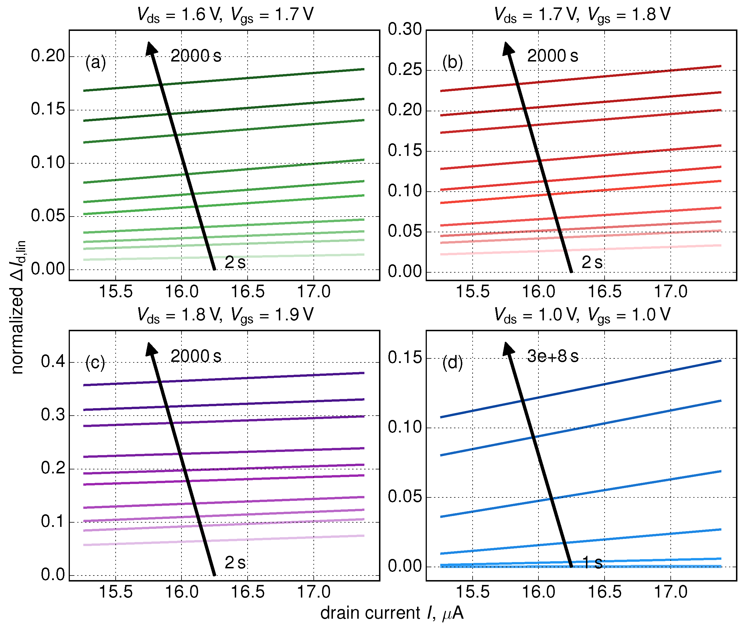
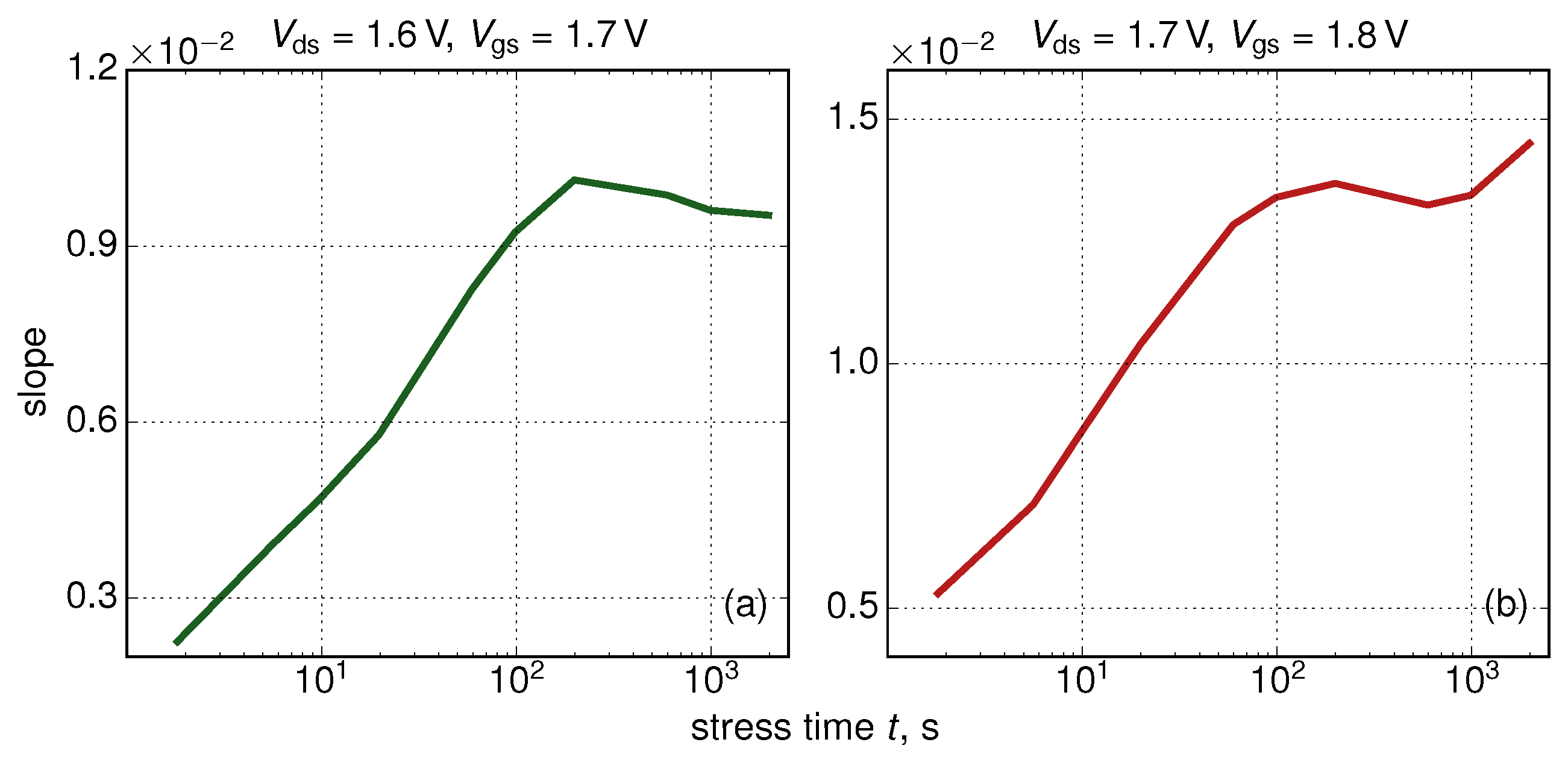
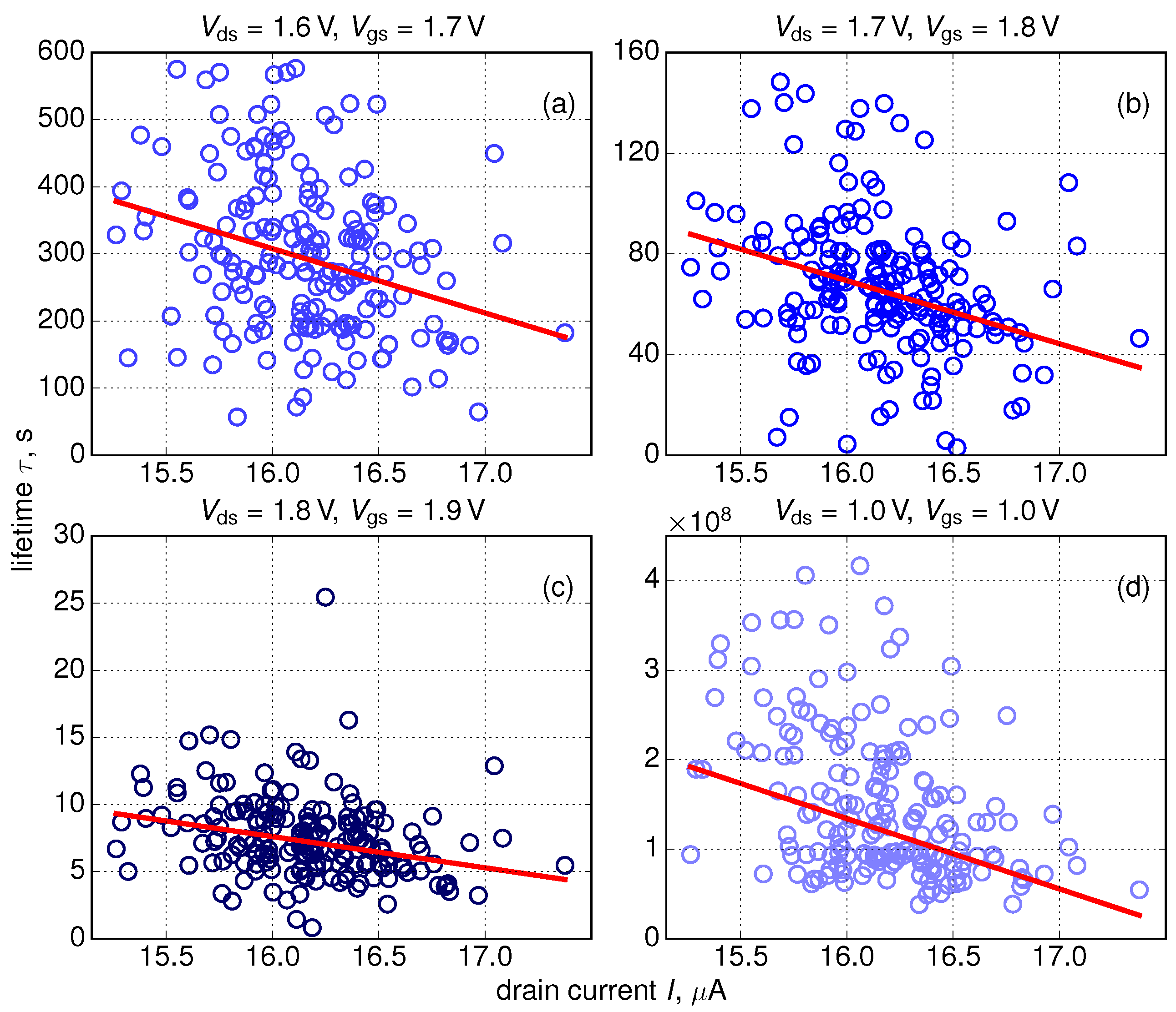
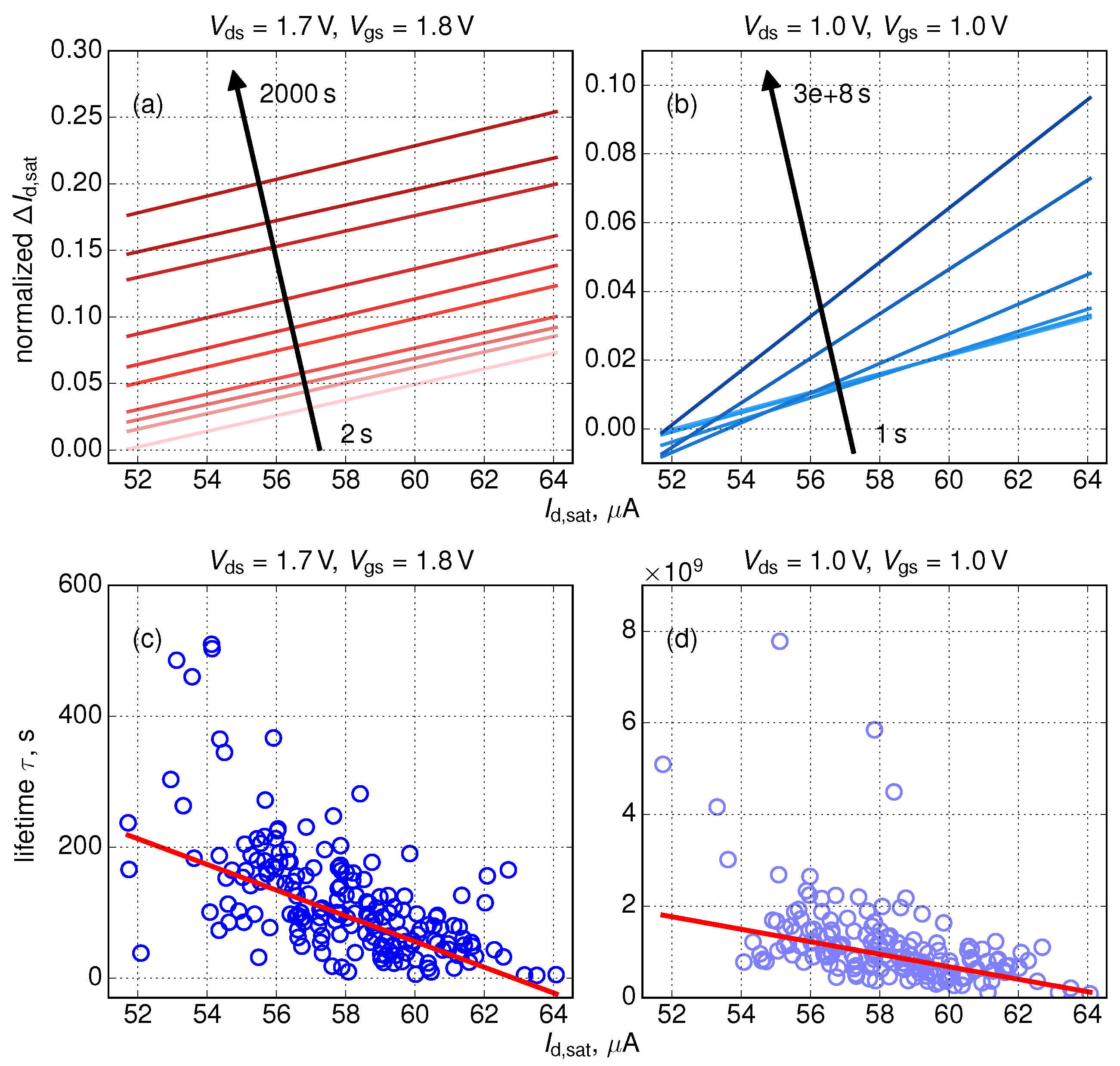
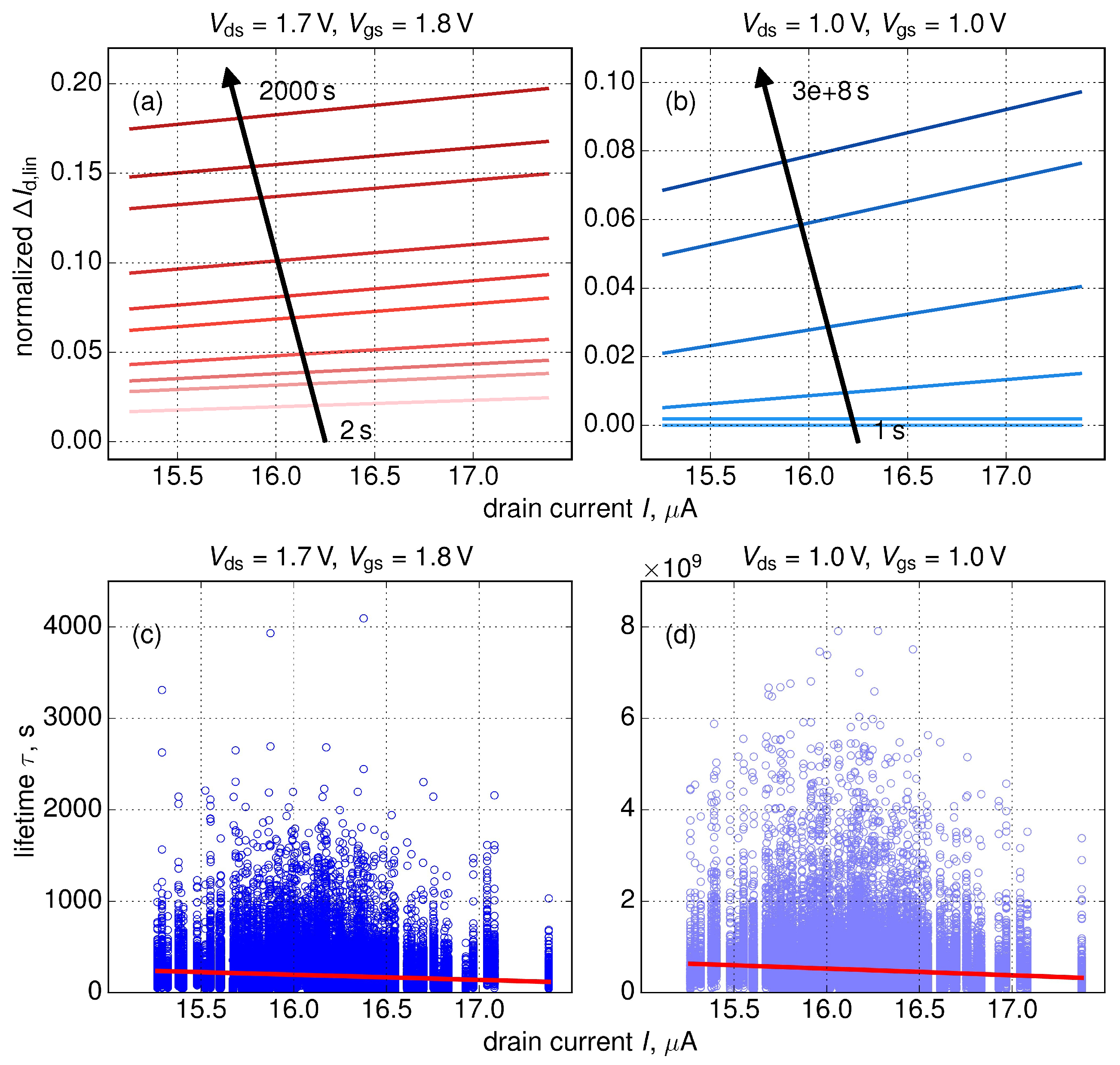
3. Results and Discussions

The distribution of the I d , lin ( 0 ) current is shown in Figure 3. As we discussed in [23,25,78], I d , lin ( 0 ) values are normally distributed and the current distribution broadens during HC stress. Such a trend can be seen in Figure 5a, which shows that the standard deviation of the linear drain current increases with stress time and this behavior is typical for all stress conditions. Quite interestingly, for much milder stress conditions with V gs = V ds = 1.0 V (close to the operating voltage) the standard deviation of I d , lin decreases with stress time. This means that in the operating regime I d , lin variability reduces and this peculiarity was reported in experimental papers by three different groups [29,31,79]. Note also that in our previous publications [23,25] we showed that degradation characteristics obtained for more aggressive HC stress conditions and at the milder operating regime obey distributions with different shapes. This is consistent with our current results.
As for the degradation traces Δ I d , lin ( t ) , their ensemble also becomes broader as can be concluded from the standard deviation of Δ I d , lin which is a growing function of t (Figure 5b). Figure 3 depicts also interface state densities N i t for V ds = 1.8 V, V gs = 1.9 V and t = 200 s evaluated for two devices, i.e., for one with I d , lin ( 0 ) equal to the mean value of the time-0 current and for a sample with a much lower initial current. One can see that in the former FinFET HCD is much more severe than in the latter device.
To study this tendency in greater detail for each of 200 instantiations we obtained Δ I d , lin changes and plotted them against I d , lin ( 0 ) current values, see Figure 6. Note that in Figure 6 we present additionally normalized changes Δ I d , lin ( t ) / Δ I d , lin (let us remind that Δ I d , lin itself is already normalized, i.e., Δ I d , lin ( t ) = | I d , lin ( t ) I d , lin ( 0 ) | / I d , lin ( 0 ) ). Due to statistical distribution of RD positions these data are very scattered and therefore—in order to extract a possible correlation between Δ I d , lin ( t ) / Δ I d , lin and I d , lin ( 0 ) —we utilized the robust linear fits employing the Kendall rank correlation coefficient [80]. Note that more advanced statistical techniques were avoided as those typically require preliminary information about the exact interrelation between variates.
This statistical analysis allowed us to extract the linear Δ I d , lin ( t ) / Δ I d , lin ( I d , lin ( 0 ) ) dependency which shows that (on average) changes in the linear drain current have larger values in devices with larger I d , lin ( 0 ) currents. In other words, we conclude that initially more performing FinFETs degrade faster than their “worse” counterparts. This trend is typical for the entire time window, as can be seen from Figure 7, where Δ I d , lin ( I d , lin ( 0 ) ) dependencies are plotted for all stress time steps. As for the slope of the Δ I d , lin ( t ) dependency (Figure 8), it increases at short stress times and then starts to decrease. This behavior is related to saturation of HCD at long times and/or high stress voltages [36,72]. Some further increase of this slope is visible in Figure 8b after ∼1 ks but we believe that this increase is related to a numerical artifact; and this increase is less than 10%.
From the calculated Δ I d , lin ( t ) traces we extracted device lifetimes τ ( τ is time at which Δ I d , lin = 0.1) and plotted them against currents in the pristine device I d , lin ( 0 ) , see Figure 9. In the same manner as for the { Δ I d , lin , I d , lin ( 0 ) } tuples we employed the Kendall rank correlation coefficient and obtained the linear interrelation between τ and I d , lin ( 0 ) which is consistent with our findings shown in Figure 6 and Figure 7, i.e., FETs with higher I d , lin ( 0 ) values degrade faster and therefore have shorter lifetimes τ .
All previous calculations were carried out based on Δ I d , lin ( t ) traces, but changes in the saturation drain current Δ I d , sat are another important metric of HCD. To show that all the trends obtained using Δ I d , lin ( t ) are typical also for Δ I d , sat ( t ) data we evaluated Δ I d , sat ( I d , sat ( 0 ) ) dependencies for all stress times and two stress conditions with V ds = 1.7 V, V gs = 1.8 V and V ds = V gs = 1.0 V, see Figure 10a,b. Using these data, lifetimes (based on the criterion of Δ I d , sat = 0.1) were extracted and summarized in Figure 10c,d. One can see that Figure 10 demonstrates exactly the same trends as those seen in Figure 7 and Figure 9. Let us note that typically Δ I d , lin values are larger than Δ I d , sat changes and therefore lifetimes extracted using the Δ I d , lin = 0.1 criterion are shorter than those which were obtained assuming Δ I d , sat = 0.1. As a consequence, the lifetime distributions presented in Figure 10c,d are shifted towards longer values as compared to the distributions shown in Figure 9b,d.
Stronger hot-carrier degradation featured by FinFETs with higher I d , lin ( 0 ) currents can be understood within our simulation framework considering coupled single- and multiple-carrier mechanisms of Si-H bond dissociation. The drain current density j d can be estimated as j d n · V gr , where n is the carrier concentration and V gr the group velocity. A higher j d value demonstrated by a certain “sample” stems from a superposition of two factors: (i) carriers have either higher densities or (ii) higher velocities (i.e., they are hotter) as compared to another instantiation. Roughly, the former aspect results in an increased rate of the multiple-carrier mechanism, while the latter one can enhance both single- and multiple-carrier mechanisms of bond rupture. Therefore we conclude that both aspects lead to accelerated HCD.
So far, we considered the impact of RDs on HCD, while the impact of random traps (RTs) was ignored. However, as we showed in our recent publications [24,26], RTs result in different shapes of Δ I d , lin and τ distributions. Nevertheless, Figure 11 shows that Δ I d , lin ( I d , lin ( 0 ) ) and τ ( I d , lin ( 0 ) ) dependencies obtained considering impacts of both RDs and RTs show the same trends as those curves generated taking only RDs into account. Note that the impact of RTs results in broadening of τ distributions, see [24,26], but this trend is a natural consequence to the fact that inclusion of RTs into our modeling approach adds an additional source of variability.

4. Conclusions

Using our statistical model for hot-carrier degradation, we generated an ensemble of 200 instantiations of the n-channel FinFET with unique random dopants configurations, calculated time-0 drain currents, their normalized changes with stress time, and extracted device lifetimes. Then, current changes were plotted vs. time-0 currents and the robust linear fit employing the Kendall rank correlation coefficient allowed us to identify correlation between these two variates. Our correlation analysis has shown that FinFETs with higher time-0 currents degrade faster and therefore have larger current changes and shorter device lifetimes. This qualitative behavior holds true for both linear and saturation drain currents (and corresponding lifetimes) and is consistent with the similar trend previously reported for bias temperature instability. Furthermore, we have shown that the impact of random traps does not changes all the aforementioned tendencies. Finally, we have showed that under stress conditions with high voltages the current distribution spreads with stress time, while in the much milder operating regime the variability of the drain current decreases. This trend agrees with our previous results showing that degradation characteristics have different distributions in stress and operating regimes.

Author Contributions

Conceptualization, all; methodology, A.M., P.R., E.B.,A.S.,B.K. and S.T.; software, A.M. and S.T.; validation, A.M., M.V., E.B., B.K. and S.T.; formal analysis, A.M., E.B., M.V., B.K. and S.T.; investigation, all; resources, A.S. and D.L.; data curation, A.M and S.T.; writing–original draft preparation, S.T.; writing–review and editing, all; visualization, A.M.; supervision, B.K., D.L. and S.T.; project administration, A.S., D.L. and S.T.; funding acquisition, S.T. All authors have read and agreed to the published version of the manuscript.

Funding

This work was supported in part by the European Union’s Horizon 2020 research and innovation programme under the Marie Sklodowska-Curie grant agreement No. 794950 and by the Austrian Science Fund (FWF), grant No. P31204-N30.

Conflicts of Interest

The authors declare no conflict of interest. The funders had no role in the design of the study; in the collection, analyses, or interpretation of data; in the writing of the manuscript, or in the decision to publish the results.

Abbreviations

The following abbreviations are used in this manuscript:
BTEBoltzmann transport equation
DFsdistribution functions
FETfield-effect transistor
HCDhot-carrier degradation
MCmultiple-carrier (machanism of bond rupture)
RDsrandom dopants
RTsrandom traps
SCsingle-carrier (mechanism of bond rupture)

References

  1. Asenov, A. Random Dopant Induced Threshold Voltage Lowering and Fluctuations in sub-0.1 μm MOSFET’s: A 3-D Atomistic Simulation Study. IEEE Trans. Electron Devices 1998, 45, 2505–2513. [Google Scholar] [CrossRef] [Green Version]
  2. Brown, A.R.; Watling, J.R.; Asenov, A.; Bersuker, G.; Zeitzoff, P. Intrinsic Parameter Fluctuations in MOSFETs due to Structural Non-uniformity of High-κ Gate Stack Materials. In Proceedings of the 2005 International Conference On Simulation of Semiconductor Processes and Devices, Tokyo, Japan, 1–3 September 2005; pp. 27–30. [Google Scholar] [CrossRef]
  3. Brown, A.R.; Watling, J.R.; Asenov, A. Intrinsic Parameter Fluctuations due to Random Grain Orientations in High-κ Gate Stacks. J. Comput. Electron. 2006, 5, 333–336. [Google Scholar] [CrossRef]
  4. Asenov, A.; Kaya, S.; Davies, J.H. Intrinsic Threshold Voltage fluctuations in Decanano MOSFETs due to Local Oxide Thickness Variations. IEEE Trans. Electron Devices 2002, 49, 112–119. [Google Scholar] [CrossRef] [Green Version]
  5. Tyaginov, S.; Vexler, M.; Shulekin, A.; Grekhov, I. Statistical Analysis of Tunnel Currents in Scaled MOS Structures with a Non-uniform Oxide Thickness Distribution. Solid State Electron. 2005, 49, 1192–1197. [Google Scholar] [CrossRef]
  6. Kaczer, B.; Franco, J.; Weckx, P.; Roussel, P.; Simicic, M.; Putcha, V.; Bury, E.; Cho, M.; Degraeve, R.; Linten, D.; et al. The Defect-Centric Perspective of Device and Circuit Reliability—From Gate Oxide Defects to Circuits. Solid-State Electron. 2016, 125, 52–62. [Google Scholar] [CrossRef]
  7. Kerber, A.; Nigam, T. Correlation of BTI induced device parameter degradation and variation in scaled Metal Gate/High-k CMOS technologies. In Proceedings of the 2014 IEEE International Reliability Physics Symposium, Waikoloa, HI, USA, 1–5 June 2014; pp. 6A.6.1–6A.6.6. [Google Scholar] [CrossRef]
  8. Kerber, A.; Srinivasan, P. Impact of Stress Mode on Stochastic BTI in Scaled MG/HK CMOS Devices. IEEE Electron Device Lett. 2014, 35, 431–433. [Google Scholar] [CrossRef]
  9. Angot, D.; Huard, V.; Rahhal, L.; Cros, A.; Federspiel, X.; Bajolet, A.; Carminati, Y.; Saliva, M.; Pion, E.; Cacho, F.; et al. BTI Variability Fundamental Understandings and Impact on Digital Logic by the Use of Extensive Dataset. In Proceedings of the 2013 IEEE International Electron Devices Meeting, Washington, DC, USA, 9–11 December 2013; pp. 15.4.1–15.4.4. [Google Scholar] [CrossRef]
  10. Hussin, R.; Amoroso, S.M.; Gerrer, L.; Kaczer, B.; Weckx, P.; Franco, J.; Vanderheyden, A.; Vanhaeren, D.; Horiguchi, N.; Asenov, A. Interplay Between Statistical Variability and Reliability in Contemporary pMOSFETs: Measurements Versus Simulations. IEEE Trans. Electron Devices 2014, 61, 3265–3273. [Google Scholar] [CrossRef]
  11. Wang, L.; Brown, A.R.; Nedjalkov, M.; Alexander, C.; Cheng, B.; Millar, C.; Asenov, A. Impact of Self-Heating on the Statistical Variability in Bulk and SOI FinFETs. IEEE Trans. Electron Devices 2015, 62, 2106–2112. [Google Scholar] [CrossRef] [Green Version]
  12. Gerrer, L.; Hussin, R.; Amoroso, S.M.; Franco, J.; Weckx, P.; Simicic, M.; Horiguchi, N.; Kaczer, B.; Grasser, T.; Asenov, A. Experimental Evidences and Simulations of Trap Generation along a Percolation Path. In Proceedings of the 2015 45th European Solid State Device Research Conference (ESSDERC), Graz, Austria, 14–18 September 2015; pp. 226–229. [Google Scholar] [CrossRef]
  13. Novak, S.; Parker, C.; Becher, D.; Liu, M.; Agostinelli, M.; Chahal, M.; Packan, P.; Nayak, P.; Ramey, S.; Natarajan, S. Transistor Aging and Reliability in 14nm Tri-gate Technology. In Proceedings of the 2015 IEEE International Reliability Physics Symposium, Monterey, CA, USA, 19–23 April 2015; pp. 2F.2.1–2F.2.5. [Google Scholar] [CrossRef]
  14. Rahman, A.; Dacuna, J.; Nayak, P.; Leatherman, G.; Ramey, S. Reliability Studies of a 10nm High-performance and Low-power CMOS Technology Featuring 3rd Generation FinFET and 5th Generation HK/MG. In Proceedings of the 2018 IEEE International Reliability Physics Symposium (IRPS), Burlingame, CA, USA, 11–15 March 2018; pp. 6F.4-1–6F.4-6. [Google Scholar] [CrossRef]
  15. Tu, C.H.; Chen, S.Y.; Chuang, A.E.; Huang, H.S.; Jhou, Z.W.; Chang, C.J.; Chou, S.; Ko, J. Transistor Variability after CHC and NBTI Stress in 90 nm pMOSFET Technology. Electron. Lett. 2009, 45, 854–856. [Google Scholar] [CrossRef]
  16. Hsieh, E.R.; Chung, S.S.; Tsai, C.H.; Huang, R.M.; Tsai, C.T.; Liang, C.W. New Observations on the Physical Mechanism of Vth-variation in Nanoscale CMOS Devices after Long Term Stress. In Proceedings of the 2011 International Reliability Physics Symposium, Monterey, CA, USA, 10–14 April 2011; pp. XT.9.1–XT.9.2. [Google Scholar] [CrossRef]
  17. Magnone, P.; Crupi, F.; Wils, N.; Tuinhout, H.P.; Fiegna, C. Characterization and Modeling of Hot Carrier-Induced Variability in Subthreshold Region. IEEE Trans. Electron Devices 2012, 59, 2093–2099. [Google Scholar] [CrossRef]
  18. Chung, S.S. The Process and Stress-induced Variability Issues of Trigate CMOS Devices. In Proceedings of the 2013 IEEE International Conference of Electron Devices and Solid-state Circuits, Hong Kong, China, 3–5 June 2013; pp. 1–2. [Google Scholar] [CrossRef]
  19. Kaczer, B.; Franco, J.; Cho, M.; Grasser, T.; Roussel, P.J.; Tyaginov, S.; Bina, M.; Wimmer, Y.; Procel, L.M.; Trojman, L.; et al. Origins and Implications of Increased Channel hot Carrier Variability in nFinFETs. In Proceedings of the 2015 IEEE International Reliability Physics Symposium, Monterey, CA, USA, 19–23 April 2015; pp. 3B.5.1–3B.5.6. [Google Scholar] [CrossRef] [Green Version]
  20. Liu, C.; Lee, K.T.; Pae, S.; Park, J. New Observations on Hot Carrier Induced Dynamic Variation in Nano-scaled SiON/poly, HK/MG and FinFET Devices Based on On-the-fly HCI Technique: The Role of Single Trap Induced Degradation. In Proceedings of the 2014 IEEE International Electron Devices Meeting, San Francisco, CA, USA, 15–17 December 2014; pp. 34.6.1–34.6.4. [Google Scholar] [CrossRef]
  21. Huard, V.; Cacho, F.; Federspiel, X.; Arfaoui, W.; Saliva, M.; Angot, D. Technology scaling and reliability: Challenges and opportunities. In Proceedings of the 2015 IEEE International Electron Devices Meeting, Washington, DC, USA, 7–9 December 2015; pp. 20.5.1–20.5.6. [Google Scholar] [CrossRef]
  22. Bottini, R.; Ghetti, A.; Vigano, S.; Valentini, M.G.; Murali, P.; Mouli, C. Non-Poissonian Behavior of Hot Carrier Degradation Induced Variability in MOSFETs. In Proceedings of the 2018 IEEE International Reliability Physics Symposium, Burlingame, CA, USA, 11–15 March 2018; pp. 6E.7-1–6E.7-6. [Google Scholar] [CrossRef]
  23. Makarov, A.; Kaczer, B.; Roussel, P.; Chasin, A.; Grill, A.; Vandemaele, M.; Hellings, G.; El-Sayed, E.M.; Grasser, T.; Linten, D.; et al. Modeling the Effect of Random Dopants on Hot-Carrier Degradation in FinFETs. In Proceedings of the 2019 IEEE International Reliability Physics Symposium (IRPS), Monterey, CA, USA, 31 March–4 April 2019; pp. 6C.3.1–6C.3.6. [Google Scholar] [CrossRef]
  24. Makarov, A.; Kaczer, B.; Roussel, P.; Chasin, A.; Vandemaele, M.; Hellings, G.; El-Sayed, A.; Jech, M.; Grasser, T.; Linten, D.; et al. Stochastic Modeling of Hot-Carrier Degradation in nFinFETs Considering the Impact of Random Traps and Random Dopants. In Proceedings of the ESSDERC 2019 - 49th European Solid-State Device Research Conference (ESSDERC), Cracow, Poland, 23–26 September 2019; pp. 262–265. [Google Scholar] [CrossRef]
  25. Makarov, A.; Kaczer, B.; Roussel, P.; Chasin, A.; Grill, A.; Vandemaele, M.; Hellings, G.; El-Sayed, A.; Grasser, T.; Linten, D.; et al. Stochastic Modeling of the Impact of Random Dopants on Hot-Carrier Degradation in n-FinFETs. IEEE Electron Device Lett. 2019, 40, 870–873. [Google Scholar] [CrossRef]
  26. Makarov, A.; Kaczer, B.; Chasin, A.; Vandemaele, M.; Bury, E.; Jech, M.; Grill, A.; Hellings, G.; El-Sayed, A.; Grasser, T.; et al. Bi-Modal Variability of nFinFET Characteristics During Hot-Carrier Stress: A Modeling Approach. IEEE Electron Device Lett. 2019, 40, 1579–1582. [Google Scholar] [CrossRef]
  27. Yu, Z.; Zhang, Z.; Sun, Z.; Wang, R.; Huang, R. On the Trap Locations in Bulk FinFETs After Hot Carrier Degradation (HCD). IEEE Trans. Electron Devices 2020, 67, 3005–3009. [Google Scholar] [CrossRef]
  28. Yu, Z.; Sun, Z.; Wang, R.; Zhang, J.; Huang, R. Hot Carrier Degradation-Induced Dynamic Variability in FinFETs: Experiments and Modeling. IEEE Trans. Electron Devices 2020, 67, 1517–1522. [Google Scholar] [CrossRef]
  29. Schlünder, C.; Berthold, J.; Proebster, F.; Martin, A.; Gustin, W.; Reisinger, H. On the Influence of BTI and HCI on Parameter Variability. In Proceedings of the 2017 IEEE International Reliability Physics Symposium, Monterey, CA, USA, 2–6 April 2017; pp. 2E-4.1–2E-4.8. [Google Scholar] [CrossRef]
  30. Ramey, S.; Chahal, M.; Nayak, P.; Novak, S.; Prasad, C.; Hicks, J. Transistor Reliability Variation Correlation to Threshold Voltage. In Proceedings of the 2015 IEEE International Reliability Physics Symposium, Monterey, CA, USA, 19–23 April 2015; pp. 3B.2.1–3B.2.6. [Google Scholar] [CrossRef]
  31. Federspiel, X.; Diouf, C.; Cacho, F.; Vincent, E. Comparison of Variability of HCI Induced Drift for SiON and HKMG Devices. In Proceedings of the International Reliability Physics Symposium, Dallas, TX, USA, 28 April–30 May 2020; pp. 5A.5.1–5A.5.5. [Google Scholar]
  32. Tyaginov, S.; Bina, M.; Franco, J.; Wimmer, Y.; Osintsev, D.; Kaczer, B.; Grasser, T. A Predictive Physical Model for Hot-Carrier Degradation in Ultra-Scaled MOSFETs. In Proceedings of the Simulation of Semiconductor Processes and Devices (SISPAD), Yokohama, Japan, 9–11 September 2014; pp. 89–92. [Google Scholar] [CrossRef]
  33. Tyaginov, S.; Jech, M.; Franco, J.; Sharma, P.; Kaczer, B.; Grasser, T. Understanding and Modeling the Temperature Behavior of Hot-Carrier Degradation in SiON nMOSFETs. IEEE Electron Device Lett. 2016, 37, 84–87. [Google Scholar] [CrossRef]
  34. Sharma, P.; Tyaginov, S.; Wimmer, Y.; Rudolf, F.; Rupp, K.; Bina, M.; Enichlmair, H.; Park, J.M.; Minixhofer, R.; Ceric, H.; et al. Modeling of Hot-Carrier Degradation in nLDMOS Devices: Different Approaches to the Solution of the Boltzmann Transport Equation. IEEE Trans. Electron Devices 2015, 62, 1811–1818. [Google Scholar] [CrossRef]
  35. Sharma, P.; Tyaginov, S.; Jech, M.; Wimmer, Y.; Rudolf, F.; Enichlmair, H.; Park, J.M.; Ceric, H.; Grasser, T. The role of cold carriers and the multiple-carrier process of Si–H bond dissociation for hot-carrier degradation in n- and p-channel LDMOS devices. Solid-State Electron. 2016, 115 Pt B, 185–191. [Google Scholar] [CrossRef]
  36. Makarov, A.; Tyaginov, S.E.; Kaczer, B.; Jech, M.; Chasin, A.; Grill, A.; Hellings, G.; Vexler, M.I.; Linten, D.; Grasser, T. Hot-Carrier Degradation in FinFETs: Modeling, Peculiarities, and Impact of Device Topology. In Proceedings of the 2017 IEEE International Electron Devices Meeting, San Francisco, CA, USA, 2–6 December 2017; pp. 13.1.1–13.1.4. [Google Scholar] [CrossRef]
  37. Vandemaele, M.; Kaczer, B.; Tyaginov, S.; Stanojević, Z.; Makarov, A.; Chasin, A.; Bury, E.; Mertens, H.; Linten, D.; Groeseneken, G. Full (Vg,Vd) Bias Space Modeling of Hot-Carrier Degradation in Nanowire FETs. In Proceedings of the 2019 IEEE International Reliability Physics Symposium, Monterey, CA, USA, 31 March–4 April 2019; pp. 1–7. [Google Scholar] [CrossRef]
  38. Rupp, K.; Grasser, T.; Jüngel, A. On the Feasibility of Spherical Harmonics Expansions of the Boltzmann Transport Equation for Three-Dimensional Device Geometries. In Proceedings of the 2011 International Electron Devices Meeting, Washington, DC, USA, 5–7 December 2011; pp. 34.1.1–34.1.4. [Google Scholar] [CrossRef]
  39. Rupp, K.; Grasser, T.; Jüngel, A. Adaptive variable-order spherical harmonics expansion of the Boltzmann Transport Equation. In Proceedings of the 2011 International Conference on Simulation of Semiconductor Processes and Devices, Osaka, Japan, 8–10 September 2011; pp. 151–154. [Google Scholar] [CrossRef]
  40. Bina, M.; Rupp, K.; Tyaginov, S.; Triebl, O.; Grasser, T. Modeling of Hot Carrier Degradation Using a Spherical Harmonics Expansion of the Bipolar Boltzmann Transport Equation. In Proceedings of the International Electron Devices Meeting, San Francisco, CA, USA, 10–13 December 2012; pp. 713–716. [Google Scholar] [CrossRef]
  41. ViennaSHE. 2014. Available online: http://viennashe.sourceforge.net/ (accessed on 1 June 2020).
  42. Tyaginov, S.; Makarov, A.; Jech, M.; Franco, J.; Sharma, P.; Kaczer, B.; Grasser, T. On the Effect of Interface Traps on the Carrier Distribution Function During Hot-Carrier Degradation. In Proceedings of the 2015 IEEE International Integrated Reliability Workshop Final Report, South Lake Tahoe, CA, USA, 9–13 October 2016; pp. 95–98. [Google Scholar] [CrossRef]
  43. Tyaginov, S.; Starkov, I.; Triebl, O.; Cervenka, J.; Jungemann, C.; Carniello, S.; Park, J.; Enichlmail, H.; Kernstock, C.; Seebacher, E.; et al. Interface Traps Density-of-states as a Vital Component for Hot-carrier Degradation Modeling. Microelectron. Reliab. 2010, 50, 1267–1272. [Google Scholar] [CrossRef]
  44. Starkov, I.; Tyaginov, S.; Enichlmair, H.; Cervenka, J.; Jungemann, C.; Carniello, S.; Park, J.; Ceric, H.; Grasser, T. Hot-Carrier degradation caused interface state profile - simulations vs. experiment. J. Vac. Sci. Technol. B 2011, 29, 01AB09-1–01AB09-8. [Google Scholar] [CrossRef]
  45. Jungemann, C.; Meinerzhagen, B. Hierarchical Device Simulation; Springer: Berlin, Germany, 2003. [Google Scholar]
  46. Brower, K. Dissociation Kinetics of Hydrogen-Passivated (111)Si-Si02 Interface Defects. Phy. Rev. B 1990, 42, 3444–3454. [Google Scholar] [CrossRef]
  47. Stesmans, A. Dissociation kinetics of hydrogen-passivated Pb defects at the (111)Si/SiO2 interface. Phys. Rev. B 2000, 61, 8393–8403. [Google Scholar] [CrossRef]
  48. Jech, M.; El-Sayed, A.M.; Tyaginov, S.; Shluger, A.L.; Grasser, T. Ab initio treatment of silicon-hydrogen bond rupture at Si/SiO2 interfaces. Phys. Rev. B 2019, 100, 195302. [Google Scholar] [CrossRef]
  49. Rauch, S.; Rosa, G.L. CMOS Hot Carrier: From Physics to End Of Life Projections, and Qualification. In Proceedings of the International Reliability Physics Symposium, tutorial, 23–25 April 2010. [Google Scholar]
  50. Bravaix, A.; Huard, V. Hot-Carrier Degradation Issues in Advanced CMOS Nodes. In Proceedings of the European Symposium on Reliability of Electron Devices Failure Physics and Analysis (ESREF), Gaeta, Italy, 11–15 October 2010; pp. 1267–1272. [Google Scholar]
  51. Tyaginov, S.; Starkov, I.; Enichlmair, H.; Park, J.; Jungemann, C.; Grasser, T. Physics-Based Hot-Carrier Degradation Models (invited). ECS Transact. 2011, 35, 321–352. [Google Scholar] [CrossRef] [Green Version]
  52. McMahon, W.; Matsuda, K.; Lee, J.; Hess, K.; Lyding, J. The Effects of a Multiple Carrier Model of Interface States Generation of Lifetime Extraction for MOSFETs. In Proceedings of the International Conference on Modeling and Simulation of Microsystem, San Juan, Puerto Rico, 21–25 April 2002; Volume 1, pp. 576–579. [Google Scholar]
  53. McMahon, W.; Hess, K. A Multi-Carrier Model for Interface Trap Generation. J. Comput. Electron. 2002, 1, 395–398. [Google Scholar] [CrossRef]
  54. Bravaix, A.; Goguenheim, D.; Revil, N.; Vincent, E.; Varrot, M.; Mortini, P. Analysis of High Temperatures Effects on Performance and Hot-Carrier Degradation in DC/AC Stressed 0.35 μm n-MOSFETs. Microel. Reliab. 1999, 39, 35–44. [Google Scholar] [CrossRef]
  55. Guerin, C.; Huard, V.; Bravaix, A. General Framework about Defect Creation at the Si/SiO2 Interface. J. Appl. Phy. 2009, 105, 114513-1–114513-12. [Google Scholar] [CrossRef]
  56. Randriamihaja, Y.; Federspiel, X.; Huard, V.; Bravaix, A.; Palestri, P. New Hot Carrier Degradation Modeling Reconsidering the Role of EES in Ultra Short n-channel MOSFETs. In Proceedings of the International Reliability Physics Symposium, Anaheim, CA, USA, 14–18 April 2013; pp. 1–5. [Google Scholar] [CrossRef]
  57. Bina, M.; Tyaginov, S.; Franco, J.; Rupp, K.; Wimmer, Y.; Osinstev, D.; Kaczer, B.; Grasser, T. Predictive Hot-Carrier Modeling of n-channel MOSFETs. IEEE Trans. Electron Devices 2014, 61, 3103–3110. [Google Scholar] [CrossRef]
  58. Tyaginov, S.; Bina, M.; Franco, J.; Osintsev, D.; Triebl, O.; Kaczer, B.; Grasser, T. Physical Modeling of Hot-Carrier Degradation for Short- and Long-Channel MOSFETs. In Proceedings of the International Reliability Physics Symposium, Waikoloa, HI, USA, 1–5 June 2014; pp. 16-1–16-8. [Google Scholar]
  59. Andrianov, I.; Saalfrank, P. Theoretical Study of Vibration-Phonon Coupling of H Adsorbed on a Si(100) Surface. J. Chem. Phys. 2006, 124, 1–10. [Google Scholar] [CrossRef]
  60. Stesmans, A. Revision of H2 Passivation of Pb Interface Defects in Standard (111)Si/SiO2. Appl. Phys. Lett. 1996, 68, 2723–2725. [Google Scholar] [CrossRef]
  61. Stesmans, A. Passivation of Pb0 and Pb1 Interface Defects in Thermal (100) Si/SiO2 with Molecular Hydrogen. Appl. Phys. Lett. 1996, 68, 2076–2078. [Google Scholar] [CrossRef]
  62. Pobegen, G.; Tyaginov, S.; Nelhiebel, M.; Grasser, T. Observation of Normally Distributed Activation Energies for the Recovery from Hot Carrier Damage. IEEE Electron Dev. Lett. 2013, 34, 939–941. [Google Scholar] [CrossRef]
  63. Stockinger, T.B.; Dragosits, K.; Grasser, T.; Klima, R.; Knaipp, M.; Kosina, H.; Mlekus, R.; Palankovski, V.; Rottinger, M.; Schrom, G.; et al. MINIMOS-NT User’s Guide; Institut für Mikroelektronik: Stuttgart, Germany, 1998. [Google Scholar]
  64. Wong, H.S.; White, M.; Krutsick, J.; Booth, R. Modeling of transconductance degradation and extraction of threshold voltage in thin oxide MOSFET’s. Solid State Electron. 1987, 30, 953–958. [Google Scholar] [CrossRef]
  65. Prakash, A.G.; Ke, S.; Siddappa, K. High-energy radiation effects on subthreshold characteristics, transconductance and mobility of n-channel MOSFETs. Semicond. Sci. Technol. 2003, 18, 1037–1042. [Google Scholar] [CrossRef]
  66. Sentaurus Process User Guide, O-2018.06; Synopsys: Mountain View, CA, USA, 2018.
  67. Next-Generation TCAD Software. Available online: http://www.globaltcad.com/en/products/minimos-nt.html (accessed on 2 June 2020).
  68. Hess, K.; Haggag, A.; McMahon, W.; Fischer, B.; Cheng, K.; Lee, J.; Lyding, L. Simulation of Si-SiO2 Defect Generation in CMOS Chips: From Atomistic Structure to Chip Failure Rates. In Proceedings of the International Electron Devices Meeting, San Francisco, CA, USA, 10–13 December 2000; pp. 93–96. [Google Scholar] [CrossRef]
  69. Bravaix, A.; Huard, V.; Goguenheim, D.; Vincent, E. Hot-Carrier to Cold-Carrier Device Lifetime Modeling with Temperature for Low power 40nm Si-Bulk NMOS and PMOS FETs. In Proceedings of the International Electron Devices Meeting, Washington, DC, USA, 5–7 December 2011; pp. 622–625. [Google Scholar] [CrossRef]
  70. Reggiani, S.; Poli, S.; Denison, M.; Gnani, E.; Gnudi, A.; Baccarani, G.; Pendharkar, S.; Wise, R. Physics-Based Analytical Model for HCS Degradation in STI-LDMOS Transistors. IEEE Trans. Electron Devices 2011, 58, 3072–3080. [Google Scholar] [CrossRef]
  71. Reggiani, S.; Barone, G.; Gnani, E.; Gnudi, A.; Baccarani, G.; Poli, S.; Wise, R.; Chuang, M.Y.; Tian, W.; Pendharkar, S.; et al. Characterization and Modeling of Electrical Stress Degradation in STI-based Integrated Power Devices. Solid State Electron. 2014, 102, 25–41. [Google Scholar] [CrossRef]
  72. Varghese, D.; Alam, M.A.; Weir, B. A generalized, IB-independent, physical HCI lifetime projection methodology based on universality of hot-carrier degradation. In Proceedings of the 2010 IEEE International Reliability Physics Symposium, Anaheim, CA, USA, 2–6 May 2010; pp. 1091–1094. [Google Scholar] [CrossRef]
  73. Lee, J.; Chen, J.; Wu, K.M.; Liu, C.; Hsu, S. Effect of hot-carrier-induced interface states distribution on linear drain current degradation in 0.35 μm n-type lateral diffused metal-oxide-semiconductor transistors. Appl. Phys. Lett. 2008, 92. [Google Scholar] [CrossRef]
  74. Chen, J.; Chen, S.Y.; Wu, K.M.; Liu, C. Investigation of hot-carrier-induced degradation mechanisms in p-type high-voltage drain extended metal-oxide-semiconductor transistors. Jpn. J. Appl. Phy. 2009, 48, 04C039. [Google Scholar] [CrossRef]
  75. Ang, D.S.; Phua, T.W.H.; Liao, H.; Ling, C.H. High-energy tail electrons as the mechanism for the worst-case hot-carrier stress degradation of the deep submicrometer N-MOSFET. IEEE Electron Device Lett. 2003, 24, 469–471. [Google Scholar] [CrossRef]
  76. Manzini, S.; Gallerano, A. Avalanche Injection of Hot Holes in the Gate Oxide of LDMOS. Solid State Electron. 2000, 44, 1325–1330. [Google Scholar] [CrossRef]
  77. Tyaginov, S.; Makarov, A.; Chasin, A.; Bury, E.; Vandemaele, M.; Jech, M.; Grill, A.; Keersgieter, A.D.; Linten, D.; Kaczer, B. Physical Modeling the Impact of Self-Heating Carrier on-Hot Degradation in pNWFETs. 2020; in press. [Google Scholar]
  78. Makarov, A.; Roussel, P.J.; Bury, E.; Vandemaele, M.; Spessot, A.; Linten, D.; Kaczer, B.; Tyaginov, S. On Correlation Between Hot-Carrier Stress Induced Device Parameter Degradation and Time-Zero Variability. In Proceedings of the IEEE International Integrated Reliability Workshop, South Lake Tahoe, CA, USA, 13–17 October 2019; pp. 1–4. [Google Scholar] [CrossRef]
  79. McMahon, W.; Mamy-Randriamihaja, Y.; Vaidyanathan, B.; Nigam, T.; Pimparkar, N. From Atoms to Circuits: Theoretical and Empirical Modeling of Hot Carrier Degradation. In Hot Carrier Degradation in Semiconductor Devices; Springer: Berlin, Germany, 2015; pp. 3–25. [Google Scholar]
  80. Kendall, M.G. A New Measure of Rank Correlation. Biometrika 1938, 30, 81–93. [Google Scholar] [CrossRef]
Figure 1. The schematic representation of our modeling framework which covers and links three main sub-tasks of the problem of hot-carrier degradation: modeling of carrier transport, modeling of the defect generation rates, and simulations of the degraded devices.
Micromachines 11 00657 g001
Figure 2. Single- and multiple-carrier mechanisms of Si-H bond rupture (left panel) and their superposition (right panel).
Micromachines 11 00657 g002
Figure 3. A sketch of the n-FinFET with random dopants (left), the distribution of the time-0 linear drain currents I d , lin ( 0 ) and N it densities obtained at V ds = 1.8 V, V gs = 1.9 V and t = 200 s for two different I d , lin ( 0 ) values (right).
Micromachines 11 00657 g003
Figure 4. Experimental and simulation Δ I d , lin ( t ) degradation traces are in good agreement for all three stress conditions. The data are from [36].
Micromachines 11 00657 g004
Figure 5. The standard deviations of the linear drain I d , lin (a) and the relative linear drain current change Δ I d , lin (b) as functions of stress time t.
Micromachines 11 00657 g005
Figure 6. Δ I d , lin ( t ) / Δ I d , lin values plotted vs. I d , lin ( 0 ) currents. Data for all four stress conditions and stress time of 2 s are shown. Note that Δ I d , lin changes are normalized to the mean linear drain current change Δ I d , lin .
Micromachines 11 00657 g006
Figure 7. Δ I d , lin ( I d , lin ( 0 ) ) dependencies for all stress time steps and four combinations of V ds , V gs . As opposed to Figure 6 showing additionally normalized Δ I d , lin ( t ) / Δ I d , lin traces this figure depicts relative changes of the linear drain current, i.e., Δ I d , lin ( t ) = | I d , lin ( t ) I d , lin ( 0 ) | / I d , lin ( 0 ) ).
Micromachines 11 00657 g007
Figure 8. The slope of the Δ I d , lin ( I d , lin ( 0 ) ) dependency as a function of stress time t for V ds = 1.6 V, V gs = 1.7 V and V ds = 1.7 V, V gs = 1.8 V.
Micromachines 11 00657 g008
Figure 9. Extracted dependencies of device lifetime τ on I d , lin ( 0 ) for all stress conditions. To evaluate device lifetime values we used a Δ I d , lin = 0.1 criterion.
Micromachines 11 00657 g009
Figure 10. Extracted Δ I d , sat ( I d , sat ( 0 ) ) dependencies for all stress time steps (a,b) and device lifetime obtained using Δ I d , sat traces (c,d).
Micromachines 11 00657 g010
Figure 11. The same as in Figure 7a,b and Figure 9c,d but considering the impact of both RDs and RTs and for two stress regimes.
Micromachines 11 00657 g011

