Materials, Design, and Characteristics of Bulk Acoustic Wave Resonator: A Review


Institute of Technological Sciences, Wuhan University, Wuhan 430072, China
*
Author to whom correspondence should be addressed.
Micromachines 2020, 11(7), 630; https://doi.org/10.3390/mi11070630
Submission received: 17 May 2020
/
Revised: 10 June 2020
/
Accepted: 18 June 2020
/
Published: 28 June 2020
(This article belongs to the Section E:Engineering and Technology)
Abstract
:With the rapid commercialization of fifth generation (5G) technology in the world, the market demand for radio frequency (RF) filters continues to grow. Acoustic wave technology has been attracting great attention as one of the effective solutions for achieving high-performance RF filter operations while offering low cost and small device size. Compared with surface acoustic wave (SAW) resonators, bulk acoustic wave (BAW) resonators have more potential in fabricating high- quality RF filters because of their lower insertion loss and better selectivity in the middle and high frequency bands above 2.5 GHz. Here, we provide a comprehensive review about BAW resonator researches, including materials, structure designs, and characteristics. The basic principles and details of recently proposed BAW resonators are carefully investigated. The materials of poly-crystalline aluminum nitride (AlN), single crystal AlN, doped AlN, and electrode are also analyzed and compared. Common approaches to enhance the performance of BAW resonators, suppression of spurious mode, low temperature sensitivity, and tuning ability are introduced with discussions and suggestions for further improvement. Finally, by looking into the challenges of high frequency, wide bandwidth, miniaturization, and high power level, we provide clues to specific materials, structure designs, and RF integration technologies for BAW resonators.
1. Introduction
The rapid development of wireless communication applications has led to the urgent requirement for wide bandwidth and high-speed data transmissions. In the field of mobile communications, the fifth generation (5G) technology is the new technology after 4G. Compared with 3G and 4G, the transmission rate and the ability to carry data of 5G networks have been greatly improved with a high utilization of spectrum resources and complex communication protocols. Nowadays, more than 30 bands are being used, and this number keeps increasing. In order to better satisfy the ever-increasing requirement, radio frequency (RF) filters have been developed dramatically.
At present, the most mainstream implementation of RF filters is dominated by surface acoustic wave (SAW) filters and bulk acoustic wave (BAW) filters. A milestone of micro RF filter technologies is presented in Figure 1. When compared with SAW filters, BAW filters are widely acknowledged because of their high operating frequency and power capacity advantages. The high-quality factor (Q-factor) of BAW makes filter skirts steeper, while high acoustic velocity and thermal conductivity enable high power handling. Additionally, the low power consumption, high isolation, and complementary metal oxide semiconductor (CMOS) compatibility of BAW filters make it a dominant device in the field of RF communications [1]. In 1999, the first commercially valuable film BAW duplexer was developed by the American company Agilent [2] and it was officially commercialized two years later [3,4]. Subsequently, lots of international well-known semiconductor companies, including Broadcom (Avago), Qorvo, Taiyo, Samsung, Infineon, STMicroelectronics, EPCOS and Fujitsu, have devoted a huge amount of effort to this area.
In many ways, the emergence for 5G is a challenge for data rates, coverage, and minimization. Firstly, the phases of 5G utilize higher radio frequencies, but the acoustic and ohmic losses increase dramatically with operating frequency of BAW filters. Secondly, the N78, N79, and N77 of 5G NR frequency bands require 500, 600, and 900 MHz of bandwidth, respectively, while obtaining a relatively large bandwidth, up to 10%, is also a difficult problem for a BAW filter based on aluminum nitride (AlN). Thirdly, considering the entire RF system, the decreasing module size and increasing input power are inevitable trends in the future.
The BAW resonator, as a basic unit of RF circuits, significantly affects the performance of BAW filters. AlN is still the preferential material for bulk production of BAW devices, but the most limiting property is probably the coupling coefficient. In this work, we summarize the existing technologies of BAW resonators, and discuss merits of various piezoelectric and electrode materials in high-coupling, large-bandwidth, high-performance designs. Next, the common methods and latest designs for optimizing the spurious mode, temperature compensation, and multi-band of the resonator are given. Finally, a new design of laterally-excited bulk-wave resonators (XBAR) with ~25% strong piezoelectric coupling and a RF integration technology are proposed for further improving the properties of BAW devices, thus enhancing the availability of BAW resonators and filters in RF communication.
2. The Basic Principle
2.1. Structure of Resonator
The BAW resonator is a piezoelectric stack structure consisting of a piezoelectric film sandwiched between two metallic electrodes. The area where the upper and lower electrodes and the piezoelectric layer overlap in the thickness direction is defined as the active area of the resonator. The FBAR (film bulk acoustic resonator) and SMR (solid mounted resonator) are two types of technology of BAW resonators (Figure 2). The fundamental resonance occurs when the wavelength of the mechanical wave generated by the excitation is twice the thickness of the piezoelectric layers. Regardless of the electrodes, the resonant frequency depends on the acoustic velocity and the thickness of the piezoelectric film:
where f0 and v are the resonant frequency and acoustic velocity, respectively, and d is the thickness of the piezoelectric film. Also, the thickness of the electrode can affect the resonant frequency. An electrode of different thickness as a mass loading can generate a frequency shift, which is often used to form the filter passband.
2.2. Equivalent Model
The physical one-dimensional Mason model and circuit-based modified Butterworth Van Dyke (MBVD) model are commonly used for BAW resonator and filter design. The input and output impedance characteristics of the resonator can be obtained directly using the Mason model with the equivalent mathematical deformation of the structure and material parameters, and the energy loss mechanism can be described by introducing a complex modulus of elasticity and a complex propagation constant [6]. The MBVD model is proposed to describe the electrical properties of BAW resonator near low frequency or resonance point (Figure 3a). The parasitic parameters Rs and R0 are introduced and used to illustrate the electrical loss of electrode and dielectric loss of piezoelectric film. Particularly, the parasitic parameters extracted by the MBVD model can be used in the Mason model for a better fit [7].
Frank Z. Bi et al. proposed a model called Rs(f)-MBVD [9] to solve the problem that the traditional MBVD model cannot fit the impedance of resonator due to spurious mode loss below fs. By replacing Rs with Rs+rs(f), where rs(f) is the introduced frequency dependent resistance, the newly improved MBVD model can predict filter passband slope distortion for filter design and optimization (Figure 3b). Seungku Lee et al. [10] proposed a nonlinear MBVD model for switchable BaxSr1-xTiO3 (BST) ferroelectric FBARs. A method for extracting the voltage-dependent (Vdc) MBVD model parameters (i.e., Lm,0, Cm,0, Rm,0, Ce,0, and Re,0) and a model applicable over a wide range of DC bias voltage is developed, as is shown in Figure 4.
2.3. Key Parameters of Bulk Acoustic Wave (BAW) Resonator
For the BAW resonator, the figure of merit (FOM) is one of the most important parameters, and can be defined as:
where keff2 is the effective coupling coefficient, and Q is the quality factor. A larger keff2 gives a wide bandwidth, which is desired for 5G band. Increasing the resonator Q-value (especially such that both Qs and Qp values are greater than 2000) is a significant goal of resonator design.
2.3.1. Effective Coupling Coefficient
Piezoelectric material-coupling coefficient kt2 and effective coupling coefficient keff2 are two different expressions. It is not hard to design a resonator with the required keff2 from a material having a quite adequate kt2 value [11]. Besides, electrode configuration, acoustic reflector, and parasitics are other major factors that can significantly influence the keff2 [12,13]. The calculation of keff2 via series resonant frequency fs and parallel resonant frequency fp is given [8]:
When AlN is deposited on the substrate, a transition region with poor crystal quality will be formed at the interface between the AlN and the substrate. The thinner this layer is, the better the overall layer coupling will be [5]. For a given material, there is always an optimum thickness ratio that maximizes the keff2 (see Figure 5b). As for electrodes, high acoustic impedance materials can boost the achievable keff2 due to the matching of the shape of the stress field and the electric field (Figure 5a). Similarly, reflector layers can cause the loss of the stress field, thereby reducing the coupling.
2.3.2. Quality Factor
The Q of a resonator is defined by the device’s loss mechanism. Various loss mechanisms are possible, including acoustic losses, ohmic losses of the electrodes and viscoelastic losses [15]. Particularly, shear waves and laterally leaking waves can constitute a major loss mechanism for BAW resonators [16,17]. The electrode of the BAW resonator is usually not equipotential, thus eddy currents are produced, leading to I2R losses and decreased Qs [18]. Because of the existence of the acoustic reflection layer, SMR-BAW may have more losses like material loss, incomplete suppression of energy loss which can flow through the reflection layer, and resistive losses from the interconnections.
Since the calculation of Q is sensitive to spurious resonance and measurement noise, there are several approaches to estimate the Q of a resonator. Methods of 3-dB bandwidth and phase derivation are sensitive to the quality of the measured data [8], and can just characterize the Q-value at fs and fp. The Bode method, or using the stored energy divide by the dissipated energy per cycle, can derive a Q that is not only at the two resonance frequencies, but also over a whole frequency range in the vicinity of those frequencies. A more specific analysis and discussion of Q have been given in [19].
2.4. Topology of Filter
The BAW filters can be basically divided in ladder and lattice topologies. Generally, ladder-type filters present a steep rejection near the passband, but a poor out-of-band rejection. A. A. Shirakawa et al. presented a combined topology (ladder-lattice) that ally the advantages of both types with high selectivity and high isolation [20]. J. Verdu et al. modified the conventional ladder-type filter in order to improve the out-of-band rejection. By adding a series/shunt inductor, a new pair of transmission zeros will appear in the transmission response [21]. Then, they also developed a double-ladder configuration based on electrically coupled BAW resonators in order to obtain a dual-band transmission [22]. Since the bonding wires from the chip to the signal ports and ground should be considered when designing filters, Alexandre A et al. used the bonding wires with an inductive effect to improve the ladder-type filter return loss and isolation, overcoming the constraints given by the inductors association [23]. Qingrui Yang et al. [24] proposed a modified lattice network with two auxiliary inductors and the measured 3-dB bandwidth can reach 12.3% at 3.25 GHz (Figure 6).
3. Materials
3.1. AlN
At present, there are mainly three kinds of piezoelectric materials used in BAW resonators: AlN, PZT, and ZnO. For PZT, although it has a high kt2 and large dielectric constant, the inherent loss of PZT is too large, the speed of sound is too low, and the preparation process is difficult to keep the composition uniform. The kt2 of ZnO is also larger than that of AlN, but its longitudinal sound velocity is much smaller than that of AlN. Furthermore, the zinc element will reduce the carrier lifetime during processing and is not compatible with CMOS technology.
AlN is a hexagonal wurtzite structure with lattice constants a = 0.322 nm and c = 0.498 nm [25]. The maximum piezoelectric response (piezoelectric strain coefficient d33 is about 5.5 pC/N [26]) can be obtained in the longitudinal direction. Simultaneously, it has high stiffness C33 (3.67 × 10¹¹ N/m2) [27], a relatively high kt2 (6.5–7%) [27], relatively high longitudinal sound velocity v (11354 m/s), and a low temperature coefficient (−25 ppm/°C or less) [28]. Other factors like the relative dielectric constant εr (about 10.2 [29]), the intrinsic Q of the material, and compatibility with CMOS processes are also consistent with the design requirement of BAW resonators and filters. Thus, piezoelectric AlN previously became the first choice for BAW resonators.
AlN thin films can be deposited by magnetron sputtering, molecular beam epitaxy, pulsed laser deposition, and metal organic chemical vapor deposition.
Among them, molecular beam epitaxy has a low deposition rate, high production cost, and poor process compatibility. Pulsed laser deposition method cannot be applied in large-area film deposition, and the thickness uniformity of the deposited film is poor. The metal organic chemical vapor deposition method is prone to cause large residual stress due to the high deposition temperature. At present, magnetron sputtering is the most used deposition method for preparing piezoelectric AlN films. It is generally performed at a lower temperature (typically 200–300 °C), and the maximum temperature is up to 400–500 °C during the reaction [30], which makes deposition processes compatible with CMOS technology and reduces deposition cycles. Besides, the method has the advantages of high efficiency, low cost, large deposition area [31], etc.
Rapid thermal annealing (RTA) after sputtering is another effective way to improve the quality of the AlN film. Vergara et al. found that after rapid annealing at 1300 °C, the intensity of the AlN (002) peak increased and the full-width half-maximum (FWHM) decreased [32]. Lin et al. used laser annealing to treat AlN. When AlN film was treated with a laser with a wavelength of 355 nm and a power of 0.025 W, the crystallinity of the film was significantly improved. The peak intensity of (002) was 58.7% higher than the untreated peak intensity [33]. However, high temperature and long treatment may have a negative impact [34], and the enhanced crystal quality of the films due to RTA hardly contributes to a significant improvement in kt2. In fact, results of RTA did not clearly describe the changes in thin film surface morphology, residual stress, and piezoelectric response, which makes RTA not used at the production level.
In addition, the quality of AlN can be also affected by the thickness of films. Some studies have shown that as the thickness of AlN increases, the FWHM 002-rocking curve of AlN film decreases, d33 increases, and the dielectric loss decreases. When the thickness increases to 1 um, the change of thickness has little effect on the quality of AlN (Figure 7).
3.2. Single Crystal AlN
Compared with poly-crystalline AlN, single crystal AlN has quantifiable higher crystal quality, fewer defects, and more stable chemical properties. Generally, (002) X-ray diffraction rocking curve FWHM of single crystal AlN can be 0.02–1°, compared with the typical FWHM of 2–3° in poly-crystalline AlN. Improved crystal quality in the single crystal AlN has been proved to result in improvements in acoustic velocity and potentially improved piezoelectric coefficients [36]. Moreover, single crystal AlN-based BAWs are superior to the poly-crystalline AlN devices. Defects existing in poly-crystalline AlN will cause absorption or scattering of bulk acoustic waves and increase acoustic transmission loss.
However, there are still many problems that directly hinder the commercialization of single crystal AlN. For example, the area of single crystal AlN that we can obtain is usually small and normally based on a 2-inch [37,38] substrate; the thickness is small, usually only 100 to 200 nm [39]; and the film deposition is expensive, slow, and conditional [40].
In 2016, a group from Akoustis Technologies Inc. presented that single crystal AlN-based devices had more than double keff2 than poly-crystalline AlN-based devices in the upper bound case, and the FOM is typically 30% higher, although the Q-value is slightly lower in single crystal devices [41]. In 2017, the same group used metal-organic chemical vapor deposition (MOCVD) to obtain single crystal epitaxial AlN film with 0.5 [42] and 0.6 [36] um thickness 4H silicon carbide (SiC) substrates with 150 mm diameter. Resonators showed keff2 of 6.32% and 7.63%, and Qmax of 1523 and 1572, respectively. In 2018, a new high-power BAW device was created on a 6-inch Si substrate with high Qmax of 3685 and FOM of 222 working at 1.8 GHz (Figure 8a) [43]. Furthermore, experiments also confirmed that single crystal AlN devices had better power handling capabilities than AlN-based devices (Figure 8b).
Moreover, Shin et al. reported the growth of single crystal AlN by magnetron sputtering. They found that pre-depositing 5 nm thick Al on the substrate before single crystal AlN deposition is critical [44], which proved that the epitaxial growth of single crystal AlN on a Si substrate at room temperature by magnetron sputtering is possible.
3.3. Doped AlN
Doping other elements into AlN is another effective method to improve the piezoelectric properties of AlN. Since Akiyama et al. found that the d33 of the piezoelectric film increased 400% after doping the Sc element [26], many efforts had been devoted to investigate the effect of doping elements on the piezoelectric properties of AlN films.
The elements include Sc [26,27,45,46,47,48,49], Ti [50,51], Ta [25,52], V [52], Y [53], Mg [54], and Er [55]. The co-doping element includes Mg+Zr [56,57], Mg+Hf [57,58], Mg+Nb [59,60], and Mg+Ti [61]. Sc, Ta, Y, and Er increase the piezoelectric properties of the film within a certain doping concentration range. Ti, V, Mg, Zr, Hf, and Nb may deteriorate the piezoelectric properties of the film. Moreover, controlling the ratio of multi-element doping, such as Mg+Zr/Hf/Nb/Ti, can also greatly improve the piezoelectric properties of the film.
The reason why doping certain elements into AlN can lead to an increase in the piezoelectric properties and kt2 of the piezoelectric film is that the lattice constant of the original unit cell will change when these elements are doped into AlN. For example, as Sc concentration increases, the lattice constant a will increase, and the lattice constant c will increase initially and decrease at a certain value of concentration. However, the overall value of c/a will decrease (Figure 9a) [26], which will cause the film to be more sensitive to pressure in the c-axis direction.
Generally, these doping elements increase the piezoelectric coefficient e33, the relative dielectric constant εr, and decrease the stiffness coefficient c33, thereby increasing the piezoelectric strain constant d33 of the material and the kt2 (d33 ≈ e33/c33 [46], kt2 = e332/(c33 × εr + e332) [27]) (see Figure 9). Unfortunately, these doping elements reduce Young’s modulus [48] of the film, the longitudinal sound velocity [62], and the temperature stability [62] of the piezoelectric film, and increase the dielectric loss [48].
On the other hand, although doping elements such as Sc can improve the piezoelectric properties of piezoelectric materials and increase the keff2 of the BAW resonator, the Q-value of the resonator is generally reduced. The reason is that the doping element will increase the dielectric loss, thus deteriorating the quality of the piezoelectric material [63]. Zywizki et al. [64] studied the effect of different Sc doping concentrations on the quality of ScAlN films. They found that the FWHM of the (002) diffraction peak increased from 0.12° to 0.52° when the concentration of Sc increased from 0% to 36.8%. As the content of Sc continued to increase, the intensity of the peak gradually decreased until it disappeared. The introduction of the Sc element not only damages the orientation of the film but also reduces the uniformity of the film due to the segregation of elements. Therefore, it is important to control the doping concentration of Sc in ScAlN film for obtaining a good performance.
3.4. Electrode Material
In addition to the influence of piezoelectric materials, the choice of the electrode materials is also important. The ideal electrode material should have high acoustic impedance (high acoustic impedance difference with piezoelectric material is beneficial to improve the effective electromechanical coupling coefficient of the resonator), low resistivity (the lower the resistivity, the smaller the Rs, which is beneficial to increase the Q-value of the resonator), and low density (higher density means higher mass loading, which is not conducive to the high frequency of the resonator). Moreover, since the piezoelectric material is directly deposited on the electrode material, the type and quality of the electrode directly affect the quality of the piezoelectric material. Good orientation, low surface roughness (reducing the scattering loss of sound waves [66]), and low lattice distortions with piezoelectric material are beneficial to improve the quality of the piezoelectric film and improve the performance of the resonator.
Many research works have studied the effects of various electrode materials, including Pt [67], Mo [66,68], W [69], Ru [70,71], Ir [72,73,74], Ta [75], Al/Au/Cu [76], CNT (carbon nanotube) [77], graphene [78,79], and ITO (indium tin oxide) [80]. Among them, Mo, W, Ru, and Ir have high Young’s modulus, but the density of W is relatively high. Al, Au, and Cu have lower resistivity, but their acoustic impedance is too low. Mo has a relatively moderate acoustic impedance, density, and resistivity, so it is the material most used as an electrode (Figure 10a). CNT and graphene are novel electrode materials, which have the advantages of low density and low electrical resistivity, but the preparation of electrodes is currently difficult.
Masanori et al. further studied the effect of Young’s modulus E and density ρ on keff2 () [71]. It was found that when the ρ is fixed, keff2 increases with the increase of the electrode Z (E increases) (Figure 10b), and when the E is fixed, the keff2 changes slightly as the electrode Z increases (ρ increases) (Figure 10c). This indicates that E plays a major role in determining the increase of keff2. It was also found that higher energy and smaller energy leakage are presented in the piezoelectric layer with higher E.
Lee et al. found that for the same material, a thin metal electrode reduces the Q-value of the resonator. The reason is that the thin film increases the resistivity of the material. Similarly, since the resistivity of W electrode is higher than that of Al electrode, even if the roughness of the W surface is low (small scattering loss), the increased ohmic loss will greatly reduce the Q-value of the resonator [66].
Akiyama et al. studied the effect of lattice matching on the growth quality of AlN. The results displayed that AlN and FCC (face-centered cubic) lattice structure of the electrode are matched very well, leading to a small FWHM of the (002) diffraction peak of AlN [76]. Table 1 summarizes the lattice structure of different metals. Yokoyama et al. studied the effect of the bottom electrode with different RMS values on the quality of the AlN film. It was found that a higher FWHM value of the (002) diffraction peak of the AlN film can be obtained with a higher root mean square (RMS) value [70]. In addition, Olivares et al. found that the surface of the bottom electrode can be cleaned by Ar+ bombardment before deposition of AlN, and the RMS value of the bottom electrode is reduced, thereby improving the quality of AlN [73]. Kamohara et al. found that a seed layer between the substrate and the bottom electrode greatly improves the quality of the bottom electrode, thus enhancing the quality of the AlN film [68,81].
4. Spurious Mode
For a BAW resonator, the spurious mode usually refers to the transverse vibration mode near the main resonance. The root source of the spurious mode is that a large number of vibration modes are coupled with the excitation electric field in a resonator of limited size [82,83]. Although these resonance peaks are relatively small, the existence of spurious modes still brings many hazards. Moreover, the spurious mode affects the keff2 and Q of the resonator. Filters constructed by those resonators have worse insertion loss, smaller bandwidth, and increased ripple in the passband. In fact, the spurious mode can be reduced by increasing the area of the resonator, but this method is contrary to the miniaturization requirements of the resonator.
There are three main methods to suppress the spurious mode: apodization [84], adjusting the dispersion curve flatness of the resonator, and using the frame structure [85].
The apodization method adjusts the shape of the electrode so that the electrode does not have parallel sides, thus prolonging the path length of the acoustic wave propagation. On the other hand, the length of the transverse resonance path at the edge of the working area is unequal to prevent the formation of resonance peaks near the longitudinal wave frequency. In 2012, Park H et al. [86] studied the effects of circular, elliptical, rectangular, and trapezoidal electrodes on the electrical properties of resonators. Experimental results showed that the electrodes with asymmetric structure have less spurious modes and higher Q-values and keff2 at the anti-resonance point than the electrodes with symmetric structure.
In general, a piezoelectric stack can only work with a certain dispersion type [87]. The method by adjusting the dispersion curve flatness is based on the dispersion curve analysis. By adjusting the flatness of the thickness extensional mode (TE1) branch of the dispersion curve, the spurious mode near the main resonance frequency is reduced. Fattinger et al. found that the dispersion type of resonator and the flatness of dispersion curve can be modified by varying the thickness of uppermost oxide in the SMR acoustic mirror [85]. The type of dispersion curve is dominated by the material properties, especially the Poisson’s ratio. When the Poisson’s ratio of the material is higher than 0.33, the resonator exhibits type I dispersion and when it is less than 0.33, the type II dispersion is achieved. For a type I dispersion curve, the cutoff frequency of the TE1 mode is greater than the cutoff frequency of the thickness shear mode (TS2) (fTE1 > fTS2), and the type II dispersion curve is just the opposite (fTE1 < fTS2) (Figure 11a). Particularly, a negative group velocity occurs on the TE1 branch when the type I dispersion curve is converted to the type II dispersion curve. The second part of the branch exhibits a positive group velocity at a high wavenumber, which may impair the electrical response of the device because the main resonant frequency corresponds to a relatively small number of waves. According to Table 2, since the Poisson’s ratio of AlN is 0.25, the AlN-based resonator generally exhibits a type II dispersion curve.
The apodization method and the flatting dispersion curve do not block the coupling of the transverse vibration and the excitation electric field, so there is still a problem about the leakage of lateral acoustic wave energy. The use of a frame structure based on the boundary conditions of the resonator directly avoids the generation of lateral acoustic waves. By analyzing and adjusting the dispersion curve of the resonator, the coupling can be blocked. At this time, the lateral displacement of the active region is uniform, called piston mode, while the displacement of the outer region is exponentially attenuated [83].
The boundary condition of the frame structure, the active area, and the outer area can be satisfied by choosing the frame structure with the appropriate width [88]. For Type I resonators, the spurious mode can be suppressed by adding a border structure to achieve the transverse wave vectors in the outer and border parts satisfying wavenumber ko imaginary and kb real, respectively [14]. It is necessary to ensure fc,b < fc,a < fc,o (Figure 11b). At this time, the border is designed to superimpose a stacked layer higher than the thickness of the resonator at the edge of the resonator, called “raised frame-like”. On the contrary, Type II resonators need to exhibit fc,b > fc,a > fc,o, which means the frame structure needs to additionally contain a structure less than the thickness of the resonator. Therefore, the structure including a negative and a positive border is proposed, called “recessed frame-like” [88]. Both structures cause an exponentially decrease in the displacement outside the resonator, thus limiting the acoustic energy in the effective area.
In fact, the above three methods are applicable in both SMR and FBAR, and can be used together. But compared with FBAR, SMR has a greater degree of freedom in adjusting the dispersion curve due to the existence of acoustic mirrors, thus the spurious mode for SMR-BAW is easier to be suppressed.
For a single raised frame, energy leakage is influenced by the size of frame. If choosing an inappropriate frame size, some unwanted Lamb mode would be activated and increase acoustic wave power loss, which leads to a low Q-value [89,90]. In order to further reduce the mode-conversion and increase reflection coefficient at the frame region, Xinyi Li et al. [91] reported a double raised border of FBAR working in type Ⅱ piston mode. Through the double raised border frame, a high Q-value resonator can be obtained because of the high reflection of first-order symmetric (S1) Lamb mode for type Ⅱ dispersion (Figure 12). However, the keff2 for a double raised border of FBAR will be reduced due to the enlargement of the non-active area. Similarly, a double-step frame with different height was proposed to reflect two Lamb modes with the largest energy at anti-resonant frequency [92]. The modified structure shows an improvement of Qa of 82% compared to the no frame design. Furthermore, the double-step frame with thick metal contributes to enhancing the Qr.
Since the frame structure strongly depends on the material and dispersion type, and will change the electrical properties of the BAW resonator, the phononic crystal structure (PnC) is proposed to suppress the spurious mode and improve the Q-value of the device. Phononic crystals use the theory of acoustic wave diffusion. This principle uses Bragg reflection to change the characteristics of the propagation medium by changing the periodicity and relative position of the scatterers. By adding the PnC structure, a bandgap can be formed on the dispersion curve, and the spurious mode in the bandgap is prohibited (Figure 13). Generally, the position of the bandgap can be adjusted be close to the main resonance frequency by controlling the structural size of the PnC [93].
5. Temperature Compensation
Since the sound velocity of material (such as AlN) becomes lower as the temperature rises, the operating frequency of a BAW resonator will become lower as the temperature increases. Generally, the method to improve the temperature coefficient of a BAW resonator is to insert a material that has a positive temperature coefficient frequency (TCF), such as silicon dioxide (SiO2), though it is known that deposition of SiO2 will decrease the keff2 and Q-value. This approach achieves temperature compensation without any feedback control and external component.
There are many factors influencing the effectiveness of temperature compensation when using SiO2 as a compensated layer, such as the deposition position and the ratio between SiO2 and negative TCF layers [94,95,96]. In the case of the position of SiO2 layer, it is usually deposited on the topmost layer in a piezoelectric stack, which can protect resonator from moisture and contamination. However, this method will increase the mass loading sensitivity, making it difficult to trim the layer to obtain a desired frequency [96]. Hao Zhang et al. [97] fabricated a TC resonator by depositing SiO2 layer between the piezoelectric film and the bottom electrode. However, the electrical field falling on the SiO2 layer makes keff2 of the resonator become smaller, and the measured Q-value also decreases. Band-pass and band-stop filters with excellent wireless interferences were designed to have a TCF of −4 ppm/ºC (Figure 14).
On the other hand, in order to achieve a zero-drift frequency of the BAW resonator, a large amount of SiO2 (large ratio between the SiO2 and piezoelectric film) is usually used, which can deadly deteriorate the electrical character of BAW. Putting SiO2 at the high stress region of BAW is an excellent method, thus a minimum amount of SiO2 is used without large keff2 reduction and Q-values loss [95]. Furthermore, a higher positive temperature compensation can be operated by using boron doped SiO2 or SiOF as the temperature compensation layer [98]. Tokihiro Nishihara et al. [99] studied three structures of TC-FBAR with SiOF layer (Figure 15a). Structure 2 and 3 eliminate the effect of parasitic capacitance, thus enhancing the keff2 of TC-BAW, although the temperature compensation effect is slightly worse. The insertion loss at 2500 MHz under the temperature changing from 25 °C to −35 °C deteriorated from 2.6 dB to 3.1 dB and from 2.4 dB and 4.2 dB for the TC-FBAR and conventional FBAR, respectively (Figure 15b). These results indicated that the modified TC-BAW can effectively improve the temperature stability.
Compared with FBAR, SMR-BAW shows a huge potential in temperature compensation when using a positive material as the low impedance layer. According to the research [98], as the number of Bragg reflection layers increases, the TCF becomes smaller. In addition, increasing the thickness of the first SiO2 layer below the piezoelectric film (d1) can also decrease TCF. But when d1 increases from 0.25λ to 0.47λ, the keff2 and Q-value decrease by about 15% and 13%, respectively. The reason is that the vibration energy stored in the first layer becomes larger, and more energy is leaked in the substrate. However, a novel design called an over-moded reflector, with SiO2 of 1/2 longitudinal acoustic wavelength thickness added to the first reflector layer in the SMR-BAW, was proposed recently. Though the thickness of the first layer of SiO2 increase, the increasing energy in SiO2 actually contributes to obtaining full temperature compensation and high Q-value [28].
M. DeMiguel et al. [100] also investigated the TCF of shear mode. They found that fully compensating the TCF of shear mode is challenging compared with longitudinal mode due to the bad response. A promising method is to make the reflector of SMR-BAW asymmetric or increase the number of the reflector layer.
One of the limitations of using positive layers is that zero TCF over a wide range cannot be achieved. Wei Pang et al. [101] raised an innovative method by integrating FBAR with an air-gap capacitor to solve this problem. The air-gap capacitor forms a cantilever and bends with the temperature changing, thus reducing the TCF of the FBAR by about 40 ppm/°C.
6. Frequency Tuning Ability
In the fabrication process of the BAW device, the resonant frequency is usually different from the target value due to the deviation in the process. Furthermore, the frequency offset caused by the temperature change, electromagnetic disturbances and aging also need to be considered. On the other hand, 5G frequency allocations for mobile phones vary widely among the world’s regions, so it is difficult for a filter with a single center frequency to cover all the bands. Considering the above two points, tunable BAW resonators and filters that can operate at different frequencies have received wide attentions in recent years.
At present, the BAW resonator tuning technology mainly includes: (1) changing the physical characteristics of the piezoelectric film by bias voltage; (2) tunable components such as passive elements; (3) a ferroelectric material with an electrostrictive effect; and (4) a micro-heater element [102] (by adjusting the temperature of the FBAR through a heater, but a relatively large electric power and time are needed to change the resonant frequency of the FBAR).
For the first method, the acoustic velocity depends on the stiffness that is a function of a direct current (DC) electric field. Thus, the resonant frequency of a BAW resonator varies as a function of applied DC voltage. However, this method can only supply a small amount of frequency tuning and requires a large DC bias [103].
Table 3 summarizes the impact of adding a series or parallel passive element to the BAW resonator. It can be clearly seen that capacitors and inductors only change one of the resonance frequencies of BAW resonator. In the case of adding a capacitance, the difference between fs and fp will be reduced, while the inductance is exactly the opposite [104,105].
However, placing discrete elements in the circuit would introduce parasitics and degrade the quality factor of the system. To avoid this disadvantage, Wanling Pan et al. [106] propose a structure with the piezoelectric plate suspended in air (or vacuum) above the bottom to form a MEMS various capacitor. This design not only reduces an assembly step during processing, but also promises a high-quality factor due to the elimination of interconnection loss. The continuous tuning range is limited to about 1.9 MHz at ~6.8 GHz with an actuation voltage of 9 V. Similarly, Wei Pang et al. [107] reported another structure of electrically tunable FBAR with an air-gap capacitor formed between the top electrode and piezoelectric film. Although integrating an air-gap capacitor in the FBAR can minimize the total size of FBAR, it may deteriorate the energy trapping in the lateral direction and make the FBAR vulnerable by the damaging effect of the surface micromachine.
Another way to realize frequency tuning is using tunable materials such as SrTiO3, BaTiO3, BaxSr1-xTiO3 (BST) to replace the piezoelectric layer of the devices. Those materials exhibit strong piezoelectric and/or electrostrictive properties. By applying a DC voltage, electromechanical coupling coefficient and sound speed of the device are changed, thereby achieving frequency shift. Particularly, because the BST thin film is the paraelectric phase, no resonance is observed at zero bias. However, with increased DC bias, the resonance develops and can be clearly tuned [108,109].
Table 4 summarizes the results of some existing studies on tunable BAW resonators using ferroelectric materials. Obviously, although those devices show some tuning abilities, the low Q-value inherent to ferroelectric materials limits the practical use.
Moreover, the characteristics of tuning abilities contributes to the design of wide bandwidth and mutli-band filters, and the conventional circuit topologies limit the achievable bandwidth of the AlN BAW filter (typically 6%). As is described in Table 3, the introduction of inductance can lead to increased keff2, thereby widening the effective bandwidth of filters. Seungku Lee et al. [116] designed and fabricated a switchable filter based on BST ferroelectric material using a 2.5-stage ladder-type configuration (Figure 16a). The filters were designed to have a 2.5% fractional bandwidth having center frequencies at 1.85, 1.96, and 2.04 GHz and provide an isolation of more than 27 dB (Figure 16b). For Carrier Aggregation (CA) applications, tuning on both channels simultaneously can achieve double/triple-band function (Figure 16c).
In fact, tuning frequency is complicated in acoustic resonators. Most of the above methods for tunable devices involve applying a variable electric field. The battery voltage of mobile phones is typically 2–3 V. In case a higher voltage is required for tuning, an intricate and space-consuming system is needed. Even if a suitable approach to tuning frequency can be found, there are many other conditions needed to be fulfilled for a tunable filter with any practical value.
7. Prospects
7.1. Lithium Niobate and Laterally-Excited Bulk-Wave Resonators (XBAR)
Lithium niobate (LN) appears to be a potential material with the form of crystalline films, due to the large value of its coupling coefficient for the fast shear mode.
In fact, the traditional BAW technology cannot cover the wider bandwidths required due to the relatively small piezoelectric coupling. Therefore, a novel device named XBAR is proposed and receive continuous attention [117,118]. As shown in Figure 17, the resonator with interdigital transducers (IDT) on a suspended LN plate can excite standing bulk acoustic shear wave resonance by applying lateral electrical field parallel to the crystalline y-axis. The curve in the cross-section diagram represents the shear deformation in the LN layer, and small arrows indicate the direction and magnitude of atomic motion. The direction of acoustic energy flow of the primary shear acoustic mode is substantially orthogonal to the surface of the piezoelectric plate [119]. Experimental data showed that the main shear resonance is at 4.55 GHz, and the third harmonic is near 13 GHz. The relative bandwidth for shear bulk wave fundamental (A1) mode is about ~11% and the coupling coefficient keff2 ≈ 25%, which absolutely satisfy the requirement for mobile phones at 4–6 GHz frequencies and even have huge potential at 10–25 GHz without harsh lithography conditions.
In addition to exciting vertical shear vibration A1 mode, there are also appearances of higher order harmonics of Lamb waves in the horizontal direction (A0, S0, A1–3, A1–5) (Figure 17c). Because the horizontal A1-3 harmonic is close to the right of anti-resonance, it may adversely affect the filter design. S. Yandrapalli et al. [120] found that changing the value of pitch and mass loading of metal electrodes can not only tune the frequency, but also adjust the relative position of A1-3 mode and anti-resonance. Furthermore, it is observed that there is no A1-3 mode at metallization of 25%, but magnitude of S0 and A0 mode increases.
A typical XBAR may have hundreds, possibly thousands, of parallel fingers in the IDT. The IDT of a XBAR differs substantially from the IDTs used in SAW resonators, which the pitch p of the IDT is typically 2 to 20 times the width w of the fingers. The width of the IDT fingers in a XBAR is not constrained to one-fourth of the acoustic wavelength at resonance [119]. However, there are still many problems to be solved for XBAR, such as poor mechanical reliability (large-size film hanging on the cavity), poor temperature coefficient of frequency, bad heat dissipation, and low power capacity. In addition, a cavity formed in the substrate can be replaced by the acoustic Bragg reflector, such as the multiple-layer structure in SMR-BAW. The acoustic Bragg reflector of SMR-XBAR [121] reflects the shear acoustic waves, thus keeping the acoustic energy predominantly confined to the piezoelectric plate. Inspired by SPH Loke’s work on two-dimensional (2D) Lamb wave resonators [122], varying the electrode dimensions and inter-electrode distancing to design two-dimensional XBARs may be an exciting idea.
7.2. Integration
In the 5G era, mobile phones need to work in multiband, which means that more RF front-end modules must be embedded in the same mobile phone space. As a result, the implementation of RF front-end systems is gradually transitioning from discrete devices to integrated chips [124]. Currently, module integration and monolithic integration are two feasible solutions.
“QM77031” is an integrated module launched by Qorvo that includes PAs, BAW filters and antenna switches. The main advantages of this product are that it can enhance performance, extend battery life, and reduce layout requirements. However, some manufacturers may feel that it has lost the flexibility of RF module design.
There are three potential monolithic integration concepts, including double-sided integration, single-sided vertical integration, and hybrid integration.
Double-sided integration mainly integrates different RF devices on the upper and lower sides of the same substrate though separate process; single-side vertical integration is a method of depositing thin films of different thicknesses on the same wafer to achieve resonators with different resonance frequencies; hybrid integration combines MEMS process and other standard process, which can integrate RF devices and IC components into a single module.
In 2018, V. Chauhan et al. [125] proposed a valuable approach to the integrated design of PA plus BAW filter architecture in two different substrate technologies (epoxy/glass and SiCer). Using the LTCC and Si part of the SiCer substrate, a hybrid integration module embedded with passive components (resistor, inductor, capacitor) was proposed with short interconnections and reduced layout parasitics (Figure 18).
8. Conclusions
As a core component of the RF front-end, acoustic resonators/filters based on BAW technology will be widely used in base stations, automotive, electronics, radar, wireless communications. AlN-based BAW devices are still one of the best choices for Sub-6GHz due to their irreplaceable superiority in performance and manufacture.
In this review, the basic principle and key parameters of the BAW resonator have been described. The literature survey provides details on the different materials, design, and characteristics of the BAW resonator. High frequency, wide bandwidth, small size, and high-power capacity are the new challenges in 5G communication networks. It is difficult to complete a high-performance filter based on conventional BAW resonator technology. Doped AlN, single AlN, and LN are preferred materials to improve the inherent performance of the resonator. Research on resonator characteristics including spurious mode, temperature compensation, and tuning ability provide technical feasibility for high-performance, stable operation and application expansion of the filter. For mobile phone applications, integration of BAW devices could be an optional solution for miniaturization targets.
Author Contributions
Conceptualization, C.S.; writing—original draft preparation, Y.L. and Y.Z.; writing—review and editing, Y.L. and Y.C.; supervision, A.T. and S.L. All authors have read and agreed to the published version of the manuscript.
Funding
This work was supported by the Hubei Provincial Major Program of Technological Innovation (No. 2019AAA052) and National Natural Science Foundation of China (No. 61974107).
Conflicts of Interest
The authors declare no conflict of interest.
References
- Ruppel, C. Acoustic Wave Filter Technology–A Review. IEEE Trans. Ultrason. Ferroelectr. Freq. Control. 2017, 64, 1390–1400. [Google Scholar] [CrossRef] [PubMed]
- Ruby, R.; Bradley, P.; Larson, J.; Oshmyansky, Y. PCS 1900 MHz duplexer using thin film bulk acoustic resonators (FBARs). Electron. Lett. 1999, 35, 794. [Google Scholar] [CrossRef]
- Feld, D.; Wang, K.; Bradley, P.; Barfknecht, A.; Ly, B.; Ruby, R. A high performance 3.0 mm X 3.0 mm X 1.1 mm FBAR full band Tx filter for US PCS handsets. In Proceedings of the 2002 IEEE Ultrasonics Symposium, Munich, Germany, 8–11 October 2002; Volume 1, pp. 913–918. [Google Scholar]
- Bradley, P.; Ruby, R.; Barfknecht, A.; Geefay, F.; Han, C.; Gan, G.; Oshmyansky, Y.; Larson, J. A 5 mm ×5 mm ×1.37 mm hermetic FBAR duplexer for PCS handsets with wafer-scale packaging. In Proceedings of the 2002 IEEE Ultrasonics Symposium, Munich, Germany, 8–11 October 2002; Volume 1, pp. 931–934. [Google Scholar]
- XBARTM Technology|Akoustis Technologies. Available online: https://akoustis.com/technology-presentations/xbaw-technology/ (accessed on 17 May 2020).
- Rosenbaum, J.F. Bulk Acoustic Waves Theory and Devices; Artech House: Norwood, MA, USA, 1988. [Google Scholar]
- Jamneala, T.; Bradley, P.; Koelle, U.B.; Chien, A. Modified Mason model for bulk acoustic wave resonators. IEEE Trans. Ultrason. Ferroelectr. Freq. Control. 2008, 55, 2025–2029. [Google Scholar] [CrossRef] [PubMed]
- Bi, F.; Barber, B. Bulk acoustic wave RF technology. IEEE Microw. Mag. 2008, 9, 65–80. [Google Scholar] [CrossRef]
- Bi, F.Z.; Barber, B.P. 11E-0 Improve MBVD Model to Consider Frequency Dependent Loss for BAW Filter Design. In Proceedings of the 2006 IEEE Ultrasonics Symposium, New York, NY, USA, 28–31 October 2007; pp. 1025–1028. [Google Scholar]
- Lee, S.; Lee, V.; Sis, S.A.; Mortazawi, A. Large-Signal Performance and Modeling of Intrinsically Switchable Ferroelectric FBARs. IEEE Trans. Microw. Theory Technol. 2012, 61, 415–422. [Google Scholar] [CrossRef]
- Hashimoto, K.-Y. RF Bulk Acoustic Wave Filters for Communications; Artech House: Norwood, MA, USA, 2009. [Google Scholar]
- Fattinger, G.G. BAW resonator design considerations—An overview. In Proceedings of the 2008 IEEE International Frequency Control Symposium, Honolulu, HI, USA, 19–21 May 2008; pp. 762–767. [Google Scholar] [CrossRef]
- Lakin, M.; Belsick, J.; McDonald, J.; McCarron, K. Improved bulk wave resonator coupling coefficient for wide bandwidth filters. In Proceedings of the 2001 IEEE Ultrasonics Symposium. Proceedings. An International Symposium (Cat. No.01CH37263), Atlanta, GA, USA, 7–10 October 2001; Volume 1, pp. 827–831. [Google Scholar] [CrossRef]
- Kaitila, J. 3C-1 Review of Wave Propagation in BAW Thin Film Devices—Progress and Prospects. In Proceedings of the 2006 IEEE Ultrasonics Symposium, Vancouver, BC, Canada, 3–6 October 2006; pp. 120–129. [Google Scholar]
- Auld, B.A. Acoustic Fields and Waves in Solids; RE Krieger: Malabar, FL, USA, 1990. [Google Scholar]
- Marksteiner, S.; Kaitila, J.; Fattinger, G.; Aigner, R.A. Optimization of acoustic mirrors for solidly mounted BAW resonators. IEEE Ultrason. Symp. 2006, 1, 329–332. [Google Scholar] [CrossRef]
- Thalhammer, R.; Aigner, R. Energy loss mechanisms in SMR-type BAW devices. IEEE MTT-S International Microw. Symp. Digest 2006, 40, 20. [Google Scholar] [CrossRef]
- Thalhammer, R.; Fattinger, G.; Handtmann, M.; Marksteiner, S. Ohmic effects in BAW-resonators. 2006 IEEE MTT-S Int. Microw. Symp. Digest 2006, 390–393. [Google Scholar] [CrossRef]
- Ruby, R. 11E-2 Review and Comparison of Bulk Acoustic Wave FBAR, SMR Technology. In Proceedings of the 2006 IEEE Ultrasonics Symposium, Vancouver, BC, Canada, 3–6 October 2006; pp. 1029–1040. [Google Scholar]
- Shirakawa, A.A.; Pham, J.-M.; Jarry, P.; Kerherve, E.; Dumont, F.; David, J.-B.; Cathelin, A. A High Isolation and High Selectivity Ladder-Lattice BAW-SMR Filter. In Proceedings of the 2006 European Microwave Conference, Manchester, UK, 10–15 September 2006; pp. 905–908. [Google Scholar]
- Verdu, J.; Menendez, O.; De Paco, P. Ladder-type filter based on bulk acoustic wave resonators with improved out-of-band rejection. Microw. Opt. Technol. Lett. 2007, 50, 103–107. [Google Scholar] [CrossRef]
- Verdu, J.; De Paco, P.; Menendez, O.; Verdu, J. Double-Ladder Filter Topology for a Dual-Band Transmission Response Based on Bulk Acoustic Wave Resonators. IEEE Microw. Wirel. Compon. Lett. 2010, 20, 151–153. [Google Scholar] [CrossRef]
- Shirakawa, A.A.; El Hassan, M.; Pham, J.-M.; Jarry, P.; Kerherve, E.; David, J.-B.; Dumont, F.; Belot, D. Method for improving ladder bulk acoustic wave filters rejection. Analog. Integr. Circuits Signal Process. 2008, 55, 69–75. [Google Scholar] [CrossRef]
- Yang, Q.; Pang, W.; Zhang, D.; Zhang, H. A Modified Lattice Configuration Design for Compact Wideband Bulk Acoustic Wave Filter Applications. Micromachines 2016, 7, 133. [Google Scholar] [CrossRef] [PubMed] [Green Version]
- Liu, H.; Zeng, F.; Tang, G.; Pan, F. Enhancement of piezoelectric response of diluted Ta doped AlN. Appl. Surf. Sci. 2013, 270, 225–230. [Google Scholar] [CrossRef]
- Akiyama, M.; Kamohara, T.; Kano, K.; Teshigahara, A.; Takeuchi, Y.; Kawahara, N. Enhancement of Piezoelectric Response in Scandium Aluminum Nitride Alloy Thin Films Prepared by Dual Reactive Cosputtering. Adv. Mater. 2008, 21, 593–596. [Google Scholar] [CrossRef] [PubMed]
- Wingqvist, G.; Tasnadi, F.; Zukauskaite, A.; Birch, J.; Arwin, H.; Hultman, L. Increased electromechanical coupling in w-ScxAl1-xN. Appl. Phys. Lett. 2010, 97, 112902. [Google Scholar] [CrossRef]
- Tajic, A. No-drift™ BAW-SMR: Over-moded reflector for temperature compensation. In Proceedings of the 2016 IEEE International Ultrasonics Symposium (IUS), Tours, France, 18–21 September 2016; pp. 1–4. [Google Scholar]
- Martin, F.; Muralt, P.; Dubois, M.-A.; Pezous, A. Thickness dependence of the properties of highly c-axis textured AlN thin films. J. Vac. Sci. Technol. A Vac. Surf. Films 2004, 22, 361–365. [Google Scholar] [CrossRef]
- Bhugra, H.; Piazza, G. Piezoelectric MEMS Resonators; Springer: Berlin/Heidelberg, Germany, 2017. [Google Scholar]
- Singh, A.V.; Chandra, S.; Bose, G. Deposition and characterization of c-axis oriented aluminum nitride films by radio frequency magnetron sputtering without external substrate heating. Thin Solid Films 2011, 519, 5846–5853. [Google Scholar] [CrossRef]
- Vergara, L.; Olivares, J.; Iborra, E.; Clement, M.; Sanz-Hervás, A.; Sangrador, J. Effect of rapid thermal annealing on the crystal quality and the piezoelectric response of polycrystalline AlN films. Thin Solid Films 2006, 515, 1814–1818. [Google Scholar] [CrossRef]
- Lin, H.-K.; Huang, Y.J.; Shih, W.C.; Chen, Y.C.; Chang, W.T. Crystalline characteristics of annealed AlN films by pulsed laser treatment for solidly mounted resonator applications. BMC Chem. 2019, 13, 30–36. [Google Scholar] [CrossRef]
- Phan, D.-T.; Chung, G.-S. The effect of geometry and post-annealing on surface acoustic wave characteristics of AlN thin films prepared by magnetron sputtering. Appl. Surf. Sci. 2011, 257, 8696–8701. [Google Scholar] [CrossRef]
- Iriarte, G.F.; Rodriguez, J.; Calle, F.; Gomez, F.C. Synthesis of c-axis oriented AlN thin films on different substrates: A review. Mater. Res. Bull. 2010, 45, 1039–1045. [Google Scholar] [CrossRef]
- Shealy, J.B.; Vetury, R.; Gibb, S.R.; Hodge, M.D.; Patel, P.; McLain, M.A.; Feldman, A.Y.; Boomgarden, M.D.; Lewis, M.P.; Hosse, B.; et al. Low loss, 3.7GHz wideband BAW filters, using high power single crystal AlN-on-SiC resonators. In Proceedings of the 2017 IEEE MTT-S International Microwave Symposium (IMS), Honololu, HI, USA, 4–9 June 2017; pp. 1476–1479. [Google Scholar] [CrossRef]
- Yang, H.; Wang, W.; Liu, Z.; Li, G. Epitaxial growth of 2 inch diameter homogeneous AlN single-crystalline films by pulsed laser deposition. J. Phys. D Appl. Phys. 2013, 46, 105101. [Google Scholar] [CrossRef]
- Yang, H.; Wang, W.; Liu, Z.; Li, G. Homogeneous epitaxial growth of AlN single-crystalline films on 2 inch-diameter Si (111) substrates by pulsed laser deposition. CrystEngComm 2013, 15, 7171. [Google Scholar] [CrossRef]
- Li, G.; Kim, T.-W.; Inoue, S.; Okamoto, K.; Fujioka, H. Epitaxial growth of single-crystalline AlN films on tungsten substrates. Appl. Phys. Lett. 2006, 89, 241905. [Google Scholar] [CrossRef]
- Wang, W.; Yang, W.; Liu, Z.; Lin, Y.; Zhou, S.; Qian, H.; Gao, F.; Yang, H.; Li, G. Epitaxial growth of homogeneous single-crystalline AlN films on single-crystalline Cu (111) substrates. Appl. Surf. Sci. 2014, 294, 1–8. [Google Scholar] [CrossRef]
- Shealy, J.B.; Shealy, J.B.; Patel, P.; Hodge, M.D.; Vetury, R.; Shealy, J.R. Single crystal aluminum nitride film bulk acoustic resonators. In Proceedings of the 2016 IEEE Radio and Wireless Symposium (RWS), Austin, TX, USA, 24–27 January 2016; pp. 16–19. [Google Scholar] [CrossRef]
- Hodge, M.D.; Vetury, R.; Gibb, S.R.; Winters, M.; Patel, P.; McLain, M.A.; Shen, Y.; Kim, D.H.; Jech, J.; Fallon, K.; et al. High rejection UNII 5.2GHz wideband bulk acoustic wave filters using undoped single crystal AlN-on-SiC resonators. In Proceedings of the 2017 IEEE International Electron Devices Meeting (IEDM); IEEE: Piscataway, NJ, USA, 2017; pp. 25.6.1–25.6.4. [Google Scholar] [CrossRef]
- Vetury, R.; Hodge, M.D.; Shealy, J.B. High Power, Wideband Single Crystal XBAW Technology for sub-6 GHz Micro RF Filter Applications. In Proceedings of the 2018 IEEE International Ultrasonics Symposium (IUS), Kobe, Japan, 22–25 October 2018; pp. 206–212. [Google Scholar] [CrossRef]
- Shin, I.-S.; Kim, J.; Lee, D.; Kim, D.; Park, Y.; Yoon, E. Epitaxial growth of single-crystalline AlN layer on Si(111) by DC magnetron sputtering at room temperature. Jpn. J. Appl. Phys. 2018, 57, 060306. [Google Scholar] [CrossRef]
- Akiyama, M.; Kano, K.; Teshigahara, A. Influence of growth temperature and scandium concentration on piezoelectric response of scandium aluminum nitride alloy thin films. Appl. Phys. Lett. 2009, 95, 162107. [Google Scholar] [CrossRef]
- Tasnadi, F.; Alling, B.; Högund, C.; Wingqvist, G.; Birch, J.; Hultman, L.; Abrikosov, I. Origin of the Anomalous Piezoelectric Response in Wurtzite ScxAl1?xN Alloys. Phys. Rev. Lett. 2010, 104, 137601. [Google Scholar] [CrossRef] [Green Version]
- Zhang, S.; Fu, W.Y.; Holec, D.; Humphreys, C.J.; Moram, M. Elastic constants and critical thicknesses of ScGaN and ScAlN. J. Appl. Phys. 2013, 114, 243516. [Google Scholar] [CrossRef]
- Akiyama, M.; Umeda, K.; Honda, A.; Nagase, T. Influence of scandium concentration on power generation figure of merit of scandium aluminum nitride thin films. Appl. Phys. Lett. 2013, 102, 21915. [Google Scholar] [CrossRef]
- Schneider, M.; DeMiguel-Ramos, M.; Flewitt, A.J.; Iborra, E.; Schmid, U. Scandium Aluminium Nitride-Based Film Bulk Acoustic Resonators. Proceedings 2017, 1, 305. [Google Scholar] [CrossRef] [Green Version]
- Iborra, E.; Capilla, J.; Olivares, J.; Clement, M.; Felmetsger, V. Piezoelectric and electroacoustic properties of Ti-doped AlN thin films as a function of Ti content. In Proceedings of the 2012 IEEE International Ultrasonics Symposium, Dresden, Germany, 7–10 October 2012; pp. 2734–2737. [Google Scholar] [CrossRef] [Green Version]
- Felmetsger, V.V.; Mikhov, M.K. Reactive sputtering of highly c-axis textured Ti-doped AlN thin films. In Proceedings of the 2012 IEEE International Ultrasonics Symposium, Dresden, Germany, 7–10 October 2012; pp. 782–785. [Google Scholar] [CrossRef]
- Iborra, E.; Olivares, J.; Clement, M.; Capilla, J.; Felmetsger, V.; Mikhov, M. Piezoelectric and electroacoustic properties of V-doped and Ta-doped AlN thin films. In Proceedings of the 2013 Joint European Frequency and Time Forum & International Frequency Control Symposium (EFTF/IFC), Prague, Czech Republic, 21–25 July 2013; pp. 262–265. [Google Scholar] [CrossRef]
- Mayrhofer, P.; Riedl, H.; Euchner, H.; Stöger-Pollach, M.; Mayrhofer, P.; Bittner, A.; Schmid, U. Microstructure and piezoelectric response of YxAl1−xN thin films. Acta Mater. 2015, 100, 81–89. [Google Scholar] [CrossRef] [Green Version]
- Anggraini, S.A.; Uehara, M.; Yamada, H.; Akiyama, M. Effect of Mg addition on the physical properties of aluminum nitride. Mater. Lett. 2018, 219, 247–250. [Google Scholar] [CrossRef]
- Hu, X.; Tai, Z.; Yang, C. Preparation and characterization of Er-doped AlN films by RF magnetron sputtering. Mater. Lett. 2018, 217, 281–283. [Google Scholar] [CrossRef]
- Yokoyama, T.; Iwazaki, Y.; Onda, Y.; Nishihara, T.; Sasajima, Y.; Ueda, M. Effect of Mg and Zr co-doping on piezoelectric AlN thin films for bulk acoustic wave resonators. IEEE Trans. Ultrason. Ferroelectr. Freq. Control. 2014, 61, 1322–1328. [Google Scholar] [CrossRef]
- Yokoyama, T.; Iwazaki, Y.; Onda, Y.; Nishihara, T.; Sasajima, Y.; Ueda, M. Highly piezoelectric co-doped AlN thin films for wideband FBAR applications. IEEE Trans. Ultrason. Ferroelectr. Freq. Control. 2015, 62, 1007–1015. [Google Scholar] [CrossRef]
- Yokoyama, T.; Iwazaki, Y.; Nishihara, T.; Tsutsumi, J. Dopant concentration dependence of electromechanical coupling coefficients of co-doped AlN thin films for BAW devices. In Proceedings of the 2016 IEEE International Ultrasonics Symposium (IUS), Tours, France, 18–21 September 2016; pp. 1–4. [Google Scholar] [CrossRef]
- Uehara, M.; Shigemoto, H.; Fujio, Y.; Nagase, T.; Aida, Y.; Umeda, K.; Akiyama, M. Giant increase in piezoelectric coefficient of AlN by Mg-Nb simultaneous addition and multiple chemical states of Nb. Appl. Phys. Lett. 2017, 111, 112901. [Google Scholar] [CrossRef]
- Tagami, K.; Koga, J.; Nohara, Y.; Usami, M. Origin of enhanced piezoelectric constants of MgNbAlN studied by first-principles calculations. Jpn. J. Appl. Phys. 2017, 56, 58004. [Google Scholar] [CrossRef]
- Anggraini, S.A.; Uehara, M.; Yamada, H.; Akiyama, M. Mg and Ti codoping effect on the piezoelectric response of aluminum nitride thin films. Scr. Mater. 2019, 159, 9–12. [Google Scholar] [CrossRef]
- Umeda, K.; Kawai, H.; Honda, A.; Akiyama, M.; Kato, T.; Fukura, T. Piezoelectric properties of ScAlN thin films for piezo-MEMS devices. In Proceedings of the 2013 IEEE 26th International Conference on Micro Electro Mechanical Systems (MEMS), Taipei, Taiwan, 20–24 January 2013; pp. 733–736. [Google Scholar]
- Fichtner, S.; Wolff, N.; Krishnamurthy, G.V.; Petraru, A.; Bohse, S.; Lofink, F.; Chemnitz, S.; Kohlstedt, H.; Kienle, L.; Wagner, B. Identifying and overcoming the interface originating c-axis instability in highly Sc enhanced AlN for piezoelectric micro-electromechanical systems. J. Appl. Phys. 2017, 122, 35301. [Google Scholar] [CrossRef]
- Zywitzki, O.; Modes, T.; Barth, S.; Bartzsch, H.; Frach, P. Effect of scandium content on structure and piezoelectric properties of AlScN films deposited by reactive pulse magnetron sputtering. Surf. Coat. Technol. 2017, 309, 417–422. [Google Scholar] [CrossRef]
- Moreira, M.; Bjurström, J.; Katardjev, I.; Yantchev, V. Aluminum scandium nitride thin-film bulk acoustic resonators for wide band applications. Vacuum 2011, 86, 23–26. [Google Scholar] [CrossRef]
- Lee, S.-H.; Yoon, K.H.; Lee, J.-K. Influence of electrode configurations on the quality factor and piezoelectric coupling constant of solidly mounted bulk acoustic wave resonators. J. Appl. Phys. 2002, 92, 4062–4069. [Google Scholar] [CrossRef]
- Muralt, P.; Antifakos, J.; Cantoni, M.; Lanz, R.; Martin, F. Is there a better material for thin film BAW applications than A1N? IEEE Ultrasonics Symposium 2006, 1, 315–320. [Google Scholar] [CrossRef]
- Kamohara, T.; Akiyama, M.; Kuwano, N. Influence of molybdenum bottom electrodes on crystal growth of aluminum nitride thin films. J. Cryst. Growth 2008, 310, 345–350. [Google Scholar] [CrossRef]
- Bradley, P.; Kim, J.; Ye, S.; Nikkel, P.; Bader, S.; Feng, C. 12E-0 2X Size and Cost Reduction of Film Bulk Acoustic Resonator (FBAR) Chips with Tungsten Electrodes for PCS/GPS/800 MHz Multiplexers. In Proceedings of the 2006 IEEE Ultrasonics Symposium, Vancouver, BC, Canada, 3–6 October 2006; pp. 1144–1147. [Google Scholar]
- Yokoyama, T.; Nishihara, T.; Taniguchi, S.; Iwaki, M.; Satoh, Y.; Ueda, M.; Miyashita, T. New electrode material for low-loss and high-Q FBAR filters. IEEE Ultrasonics Symposium 2005, 1, 429–432. [Google Scholar] [CrossRef]
- Ueda, M.; Nishihara, T.; Taniguchi, S.; Yokoyama, T.; Tsutsumi, J.; Iwaki, M.; Satoh, Y. Film Bulk Acoustic Resonator using High-Acoustic-Impedance Electrodes. Jpn. J. Appl. Phys. 2007, 46, 4642–4646. [Google Scholar] [CrossRef]
- Iborra, E.; Clement, M.; Olivares, J.; Sangrador, J.; Rimmer, N.; Rastogi, A. 7E-6 Aluminum Nitride Bulk Acoustic Wave Devices with Iridium Bottom Electrodes. In Proceedings of the 2006 IEEE Ultrasonics Symposium, Vancouver, BC, Canada, 3–6 October 2006; pp. 616–619. [Google Scholar]
- Olivares, J.; Clement, M.; Iborra, E.; González-Castilla, S.; Rimmer, N.; Rastogi, A. P1G-2 Assessment of Aluminum Nitride Films Sputtered on Iridium Electrodes. In Proceedings of the 2006 IEEE Ultrasonics Symposium, Vancouver, BC, Canada, 3–6 October 2006; pp. 1401–1404. [Google Scholar]
- Clement, M.; Iborra, E.; Olivares, J.; Rimmer, N.; Giraud, S.; Bila, S.; Reinhardt, A. DCS Tx filters using AlN resonators with iridium electrodes. IEEE Trans. Ultrason. Ferroelectr. Freq. Control. 2010, 57, 518–523. [Google Scholar] [CrossRef]
- Akiyama, M.; Ueno, N.; Nagao, K.; Yamada, T. Growth of highly c-axis oriented aluminum nitride thin films on β-tantalum bottom electrodes. J. Mater. Sci. 2006, 41, 4691–4694. [Google Scholar] [CrossRef]
- Akiyama, M.; Nagao, K.; Ueno, N.; Tateyama, H.; Yamada, T. Influence of metal electrodes on crystal orientation of aluminum nitride thin films. Vacuum 2004, 74, 699–703. [Google Scholar] [CrossRef]
- Garcia-Gancedo, L.; Al-Naimi, F.; Flewitt, A.J.; Milne, W.I.; Ashley, G.M.; Luo, J.; Zhao, X.; Lu, J.R. Fabrication of high-Q film bulk acoustic resonator (FBAR) filters with carbon nanotube (CNT) electrodes. In Proceedings of the 2010 IEEE International Ultrasonics Symposium, San Diego, CA, USA, 11–14 October 2010; pp. 301–304. [Google Scholar]
- Knapp, M.D.; Hoffmann, R.; Lebedev, V.; Cimalla, V.; Ambacher, O. Graphene as an active virtually massless top electrode for RF solidly mounted bulk acoustic wave (SMR-BAW) resonators. Nanotechnology 2018, 29, 105302. [Google Scholar] [CrossRef] [PubMed]
- Knapp, M.; Lebedev, V.; Cimalla, V.; Arnbacher, O. Metallization Design Investigations for Graphene as a Virtually Massless Electrode Material for 2.1 GHz Solidly Mounted (BAW-SMR) Resonators. In Proceedings of the 2018 IEEE International Frequency Control Symposium (IFCS), Olympic Valley, CA, USA, 21–24 May 2018; pp. 1–5. [Google Scholar] [CrossRef]
- DeMiguel-Ramos, M.; Rughoobur, G.; Flewitt, A.J.; Mirea, T.; Diaz-Duran, B.; Olivares, J.; Clement, M.; Iborra, E. Transparent thin film bulk acoustic wave resonators. In Proceedings of the 2016 European Frequency and Time Forum (EFTF), York, UK, 4–7 April 2016; pp. 1–4. [Google Scholar] [CrossRef]
- Kamohara, T.; Akiyama, M.; Ueno, N.; Nonaka, K.; Tateyama, H. Growth of highly c-axis-oriented aluminum nitride thin films on molybdenum electrodes using aluminum nitride interlayers. J. Cryst. Growth 2005, 275, 383–388. [Google Scholar] [CrossRef]
- Pensala, T.; Ylilammi, M. Spurious Resonance Suppression in Gigahertz-Range ZnO Thin-Film Bulk Acoustic Wave Resonators by the Boundary Frame Method: Modeling and Experiment. IEEE Trans. Ultrason. Ferroelectr. Freq. Control 2009, 56, 1731–1744. [Google Scholar] [CrossRef]
- Kaitila, J.; Ylilammi, M.; Ella, J.; Aigner, R. Spurious resonance free bulk acoustic wave resonators. IEEE Symp. Ultrason. 2004, 1, 84–87. [Google Scholar] [CrossRef]
- Link, A.; Schmidhammer, E.; Heinze, H.; Mayer, M.; Bader, B.; Weigel, R. Appropriate Methods to Suppress Spurious FBAR Modes in Volume Production. In Proceedings of the 2006 IEEE MTT-S International Microwave Symposium Digest, San Francisco, CA, USA, 11–16 June 2006; pp. 394–397. [Google Scholar] [CrossRef]
- Fattinger, G.; Marksteiner, S.; Kaitila, J.; Aigner, R. Optimization of acoustic dispersion for high performance thin film BAW resonators. IEEE Ultrason. Symp. 2006, 2, 1175–1178. [Google Scholar] [CrossRef]
- Park, H.; Song, I.; Shin, J.-S.; Lee, M.-C.; Son, S.U.; Kim, C.-S.; Kim, D.-H.; Cui, J. Advanced lateral structures of BAW resonator for spurious mode suppression. In Proceedings of the 2012 42nd European Microwave Conference, Amsterdam, The Netherlands, 29 October–1 November 2012; pp. 104–107. [Google Scholar]
- Fattinger, G.; Tikka, P. Laser measurements and simulations of FBAR dispersion relation. In Proceedings of the 2001 IEEE MTT-S International Microwave Sympsoium Digest (Cat. No.01CH37157), Phoenix, AZ, USA, 20–24 May 2001; Volume 1, pp. 371–374. [Google Scholar] [CrossRef]
- Thalhammer, R.; Kaitila, J.; Zieglmeier, S.; Elbrecht, L. 4E-3 Spurious Mode Suppression in BAW Resonators. In Proceedings of the 2006 IEEE Ultrasonics Symposium, Vancouver, BC, Canada, 3–6 October 2006; pp. 456–459. [Google Scholar]
- Feng, H. Thin film bulk acoustic resonator with a mass loaded perimeter. J. Acoust. Soc. Am. 2008, 123, 1227. [Google Scholar] [CrossRef]
- Jamneala, T.; Ruby, R.C. Piezoelectric Resonator Structures and Electrical Filters Having Frame Elements. U.S. Patents 8,981,876, 17 March 2015. [Google Scholar]
- Li, X.; Bao, J.-F.; Huang, Y.; Zhang, B.; Tang, G.; Omori, T.; Hashimoto, K.-Y. Use of double-raised-border structure for quality factor enhancement of type II piston mode FBAR. In Proceedings of the 2017 Joint Conference of the European Frequency and Time Forum and IEEE International Frequency Control Symposium (EFTF/IFC), Besançon, France, 9–13 July 2017; pp. 547–550. [Google Scholar]
- Nguyen, N.; Johannessen, A.; Hanke, U. Design of high-Q Thin Film Bulk Acoustic resonator using dual-mode reflection. In Proceedings of the 2014 IEEE International Ultrasonics Symposium, Chicago, IL, USA, 3–6 September 2014; pp. 487–490. [Google Scholar] [CrossRef]
- Serhane, R.; Hadj-Larbi, F.; Hassein-Bey, A.; Khelif, A. Selective Band Gap to Suppress the Spurious Acoustic Mode in Film Bulk Acoustic Resonator Structures. J. Vib. Acoust. 2018, 140, 031018. [Google Scholar] [CrossRef]
- Lakin, K.; McCarron, K.; McDonald, J. Temperature compensated bulk acoustic thin film resonators. In Proceedings of the 2000 IEEE Ultrasonics Symposium. Proceedings. An International Symposium (Cat. No.00CH37121), San Juan, Puerto Rico, 22–25 October 2002; Volume 1, pp. 855–858. [Google Scholar] [CrossRef]
- Allah, M.A.; Kaitila, J.; Thalhammer, R.; Weber, W.; Schmitt-Landsiedel, D. Temperature compensated solidly mounted bulk acoustic wave resonators with optimum piezoelectric coupling coefficient. In Proceedings of the 2009 IEEE International Electron Devices Meeting (IEDM), Baltimore, MD, USA, 7–9 December 2009; pp. 1–4. [Google Scholar] [CrossRef]
- Hu, N.; Zhou, C.; Pang, W.; Zhang, H. Temperature compensated band-pass and band-stop bulk-acoustic-wave filters solution reducing interference in wireless systems. In Proceedings of the Asia-Pacific Microwave Conference 2011, Melbourne, Australia, 5–8 December 2011; pp. 1102–1105. [Google Scholar]
- Zhang, H.; Yang, Q.; Pang, W.; Ma, J.-G.; Yu, H. Temperature Stable Bulk Acoustic Wave Filters Enabling Integration of a Mobile Television Function in UMTS System. IEEE Microw. Wirel. Components Lett. 2012, 22, 239–241. [Google Scholar] [CrossRef]
- Zou, Q.; Small, M.; Lee, D.; Bi, F.; Snyder, R.; Lamers, T.L.; Choy, J.; Ruby, R. Impact on film bulk acoustic resonator tempco and quality factor from boron doped SiO2 temperature compensation material. In Proceedings of the 2013 Transducers & Eurosensors XXVII: The 17th International Conference on Solid-State Sensors, Actuators and Microsystems (TRANSDUCERS & EUROSENSORS XXVII), Barcelona, Spain, 16–20 June 2013; pp. 1388–1391. [Google Scholar]
- Nishihara, T.; Taniguchi, S.; Ueda, M. Increased piezoelectric coupling factor in temperature-compensated film bulk acoustic resonators. In Proceedings of the 2015 IEEE International Ultrasonics Symposium (IUS), Taipei, Taiwan, 21–24 October 2015; pp. 1–4. [Google Scholar] [CrossRef]
- Ramos, M.D.M.; Olivares, J.; Mirea, T.; Clement, M.; Iborra, E.; Rughoobur, G.; Garcia-Gancedo, L.; Flewitt, A.J.; Milne, W. The influence of acoustic reflectors on the temperature coefficient of frequency of solidly mounted resonators. In Proceedings of the 2014 IEEE International Ultrasonics Symposium, Chicago, IL, USA, 3–6 September 2014; pp. 1472–1475. [Google Scholar] [CrossRef]
- Pang, W.; Yu, H.; Zhang, H.; Kim, E.S. Electrically tunable and temperature compensated FBAR. IEEE MTT-S Int. Microw. Symp. Dig. 2006, 1279–1282. [Google Scholar] [CrossRef]
- Ruby, R.; Merchant, P. Micromachined thin film bulk acoustic resonators. In Proceedings of the IEEE 48th Annual Symposium on Frequency Control, Boston, MA, USA, 1–3 June 1994; pp. 135–138. [Google Scholar]
- Stokes, R.B.; Crawford, J.D.; Cushman, D.; Kong, A.M. Thin Film Voltage-Tuned Semiconductor Bulk Acoustic Resonator (SBAR). US Patents 5,446,306, 29 August 1995. [Google Scholar]
- Razafimandimby, S.; Tilhac, C.; Cathelin, A.; Kaiser, A.; Belot, D. A novel architecture of a tunable bandpass BAW-filter for a WCDMA transceiver. Analog. Integr. Circuits Signal Process. 2006, 49, 237–247. [Google Scholar] [CrossRef]
- Tsai, H.-Y.; Wu, R.-B. Tunable filter by FBAR using coupling capacitors. In Proceedings of the 2018 Asia-Pacific Microwave Conference (APMC), Kyoto, Japan, 6–9 November 2018; pp. 1–3. [Google Scholar]
- Pan, W.; Soussan, P.; Nauwelaers, B.; Tilmans, H.A. A surface micromachined electrostatically tunable film bulk acoustic resonator. Sens. Actuators A Phys. 2006, 126, 436–446. [Google Scholar] [CrossRef]
- Pang, W.; Zhang, H.; Yu, H.; Lee, C.-Y.; Kim, E.S. Electrical Frequency Tuning of Film Bulk Acoustic Resonator. J. Microelectromechanical. Syst. 2007, 16, 1303–1313. [Google Scholar] [CrossRef]
- Berge, J.; Vorobiev, A.; Steichen, W.; Gevorgian, S. Tunable Solidly Mounted Thin Film Bulk Acoustic Resonators Based on BaxSr1-xTiO3 Films. IEEE Microw. Wirel. Compon. Lett. 2007, 17, 655–657. [Google Scholar] [CrossRef]
- Noeth, A.; Yamada, T.; Muralt, P.; Tagantsev, A.K.; Setter, N. Tunable thin film bulk acoustic wave resonator based on BaxSr1-xTiO3 thin film. IEEE Trans. Ultrason. Ferroelectr. Freq. Control. 2010, 57, 379–385. [Google Scholar] [CrossRef]
- Saddik, G.N.; Boesch, D.S.; Stemmer, S.; York, R.A. dc electric field tunable bulk acoustic wave solidly mounted resonator using SrTiO3. Appl. Phys. Lett. 2007, 91, 043501. [Google Scholar] [CrossRef]
- Vorobiev, A.K.; Gevorgian, S. Tunable thin film bulk acoustic wave resonators with improved Q-factor. Appl. Phys. Lett. 2010, 96, 212904. [Google Scholar] [CrossRef] [Green Version]
- Vorobiev, A.K.; Gevorgian, S.; Löffler, M.; Olsson, E. Correlations between microstructure and Q-factor of tunable thin film bulk acoustic wave resonators. J. Appl. Phys. 2011, 110, 054102. [Google Scholar] [CrossRef] [Green Version]
- Berge, J.; Gevorgian, S. Tunable bulk acoustic wave resonators based on Ba 0.25 Sr 0.75 TiO 3 thin films and a HfO 2/SiO 2 Bragg reflector. IEEE Trans. Ultrason. Ferroelectr. Freq. Control 2011, 58, 2768–2771. [Google Scholar] [CrossRef] [PubMed]
- Vorobiev, A.; Gevorgian, S. Enhanced tunable performance of high Q-factor BaxSr1−xTiO3 film bulk acoustic wave resonators. Int. J. Microw. Wirel. Technol. 2013, 5, 361–369. [Google Scholar] [CrossRef] [Green Version]
- Mansour, A.A.; Kalkur, T.S. High-Quality-Factor and Low-Temperature-Dependence SMR FBAR Based on BST Using MOD Method. IEEE Trans. Ultrason. Ferroelectr. Freq. Control. 2017, 64, 452–462. [Google Scholar] [CrossRef] [PubMed]
- Koohi, M.Z.; Mortazawi, A. Intrinsically Switchable Filter Bank Employing Ferroelectric Barium Strontium Titanate. IEEE Trans. Microw. Theory Tech. 2018, 66, 5501–5507. [Google Scholar] [CrossRef]
- Plessky, V.; Yandrapalli, S.; Turner, P.J.; Villanueva, L.; Koskela, J.; Hammond, R.; Plesski, V.; Villanueva, G. 5 GHz laterally-excited bulk-wave resonators (XBARs) based on thin platelets of lithium niobate. Electron. Lett. 2019, 55, 98–100. [Google Scholar] [CrossRef]
- Faizan, M.; De Pastina, A.; Yandrapalli, S.; Turner, P.J.; Hammond, R.B.; Plessky, V.; Villanueva, L.G. Fabrication of Lithium Niobate Bulk Acoustic Resonator For 5G Filters. In Proceedings of the 2019 20th International Conference on Solid-State Sensors, Actuators and Microsystems & Eurosensors XXXIII (TRANSDUCERS & EUROSENSORS XXXIII), Berlin, Germany, 23–27 June 2019; pp. 1752–1755. [Google Scholar]
- Plesski, V. Transversely-Excited Film Bulk Acoustic Resonators for High Power Applications. US Patents 16/578,811, 16 January 2020. [Google Scholar]
- Yandrapalli, S.; Plessky, V.; Koskela, J.; Yantchev, V.; Turner, P.; Villanueva, L.G. Analysis of XBAR resonance and higher order spurious modes. In Proceedings of the 2019 IEEE International Ultrasonics Symposium (IUS), Glasgow, Scotland, UK, 6–9 October 2019; pp. 185–188. [Google Scholar]
- Plesski, V. Solidly-Mounted Transversely-Excited Film Bulk Acoustic Resonator. US Patents 10,601,392, 24 March 2020. [Google Scholar]
- Loke, S.P.H.; Sun, C.; Zhu, Y.; Wang, N.; Gu, Y.A. Two dimensional, high electromechanical coupling aluminium nitride Lamb wave resonators. In Proceedings of the 2015 IEEE International Conference on Electron Devices and Solid-State Circuits (EDSSC), Chengdu, China, 1–4 June 2015; pp. 733–735. [Google Scholar]
- White Paper: Resonant Inc. (RESN). Available online: https://www.resonant.com/resources/white-papers (accessed on 17 May 2020).
- Aigner, R.; Fattinger, G. 3G—4G—5G: How Baw Filter Technology Enables a Connected World. In Proceedings of the 2019 20th International Conference on Solid-State Sensors, Actuators and Microsystems & Eurosensors XXXIII (TRANSDUCERS & EUROSENSORS XXXIII), Berlin, Germany, 23–27 June 2019; pp. 523–526. [Google Scholar]
- Chauhan, V.; Wandji, L.W.; Peng, X.; Cortes, V.S.; Frank, A.; Fischer, M.; Stehr, U.; Weigel, R.; Hagelauer, A. Design and Performance of Power Amplifier Integration with BAW Filter on a Silicon-Ceramic Composite and Standard Epoxy/Glass Substrate. In Proceedings of the 2018 IEEE MTT-S International Microwave Workshop Series on Advanced Materials and Processes for RF and THz Applications (IMWS-AMP), Ann Arbor, MI, USA, 16–18 July 2018; pp. 1–3. [Google Scholar] [CrossRef]
Figure 1.
Market application and band allocation of radio frequency (RF) filter technologies [5].
Figure 1.
Market application and band allocation of radio frequency (RF) filter technologies [5].

Figure 2.
Structure of (a) the film bulk acoustic resonator (FBAR) formed over an air gap and (b) the solid mounted resonator (SMR) formed over a Bragg reflection layer.
Figure 2.
Structure of (a) the film bulk acoustic resonator (FBAR) formed over an air gap and (b) the solid mounted resonator (SMR) formed over a Bragg reflection layer.

Figure 3.
(a) Modified Butterworth Van Dyke (MBVD) model [8]. (b) Measured filter data of Rs(f)-MBVD model, reproduced with permission from [9].

Figure 4.
(a) Nonlinear MBVD model. (b) The measured and modeled reflection coefficients on the Smith chart with DC bias voltages. Reproduced with permission from [10].
Figure 4.
(a) Nonlinear MBVD model. (b) The measured and modeled reflection coefficients on the Smith chart with DC bias voltages. Reproduced with permission from [10].

Figure 5.
(a) Stress field distribution throughout a bulk acoustic wave (BAW) resonator with low impedance and high impedance electrode materials, reproduced with permission from [12]. (b) Relationship between keff2 and the ratio of electrode thickness to total stack thickness for an AlN resonator with different electrode materials, reproduced with permission from [14].

Figure 6.
(a) Topologies of ladder type, lattice type, modified lattice with two auxiliary inductors, and their electrical responses [24]. (b) Board assembly of the filter with balun circuits [24]. Reproduced with permission from [24].

Figure 7.
Effects of different thicknesses of AlN. (a) Rocking curve full-width half-maximum (FWHM) on different substrates, reproduced with permission from [35]. (b) Piezoelectric coefficient d33, reproduced with permission from [29]. (c) Permittivity (εAlN solid circles) and dielectric loss (Tan δ, open squares), reproduced with permission from [29]

Figure 8.
(a) Q-value and figure of merit (FOM) as functions of frequency when using XBARTM (single crystal AlN technology) [43]. (b) Measured power level capability of single crystal AlN and poly-crystalline AlN [43]. Reproduced with permission from [43].

Figure 9.
Effects of different Sc doping concentrations. (a) Lattice constant a, c, c/a value, reproduced with permission from [26]. (b) Piezoelectric constant e33 and stiffness coefficient c33, reproduced with permission from [46]. (c) Piezoelectric strain coefficient d33, reproduced with permission from [45]. (d) Electromechanical coupling coefficient kt2, reproduced with permission from [65]. (e) Measured FBAR impedance curve, reproduced with permission from [65].

Figure 10.
(a) Acoustic impedance, Young’s modulus, and density of electrode materials [71]. Relationship between keff2 and normalized acoustic impedance with (b) ρ fixed and (c) E fixed [71]. Reproduced with permission from [71].

Figure 11.
(a) Influence of the Poisson ratio onto the dispersion type of a BAW resonator. Poisson ration is used to correlate the longitudinal wave velocity and the shear wave velocity of the material, reproduced with permission from [85]. (b) The structure of suppression of the type I resonator and the cut-off frequency diagram, reproduced with permission from [14].

Figure 12.
(a) BAW resonator with double raised frame [91]. (b) Admittance curves of structures with the double raised frame, the single raised frame, and without the recessed frame [91]. Reproduced with permission from [91].

Figure 13.
(a) Dispersion curve of acoustic waves in the FBAR; the formation of PnC directly bans the TE1 spurious mode generation at the antiresonance frequency [93]. (b) Comparison between the calculated input admittances of FBAR without PnC and with PnC. The resonant frequency decreases due to the mass-loading effect, and the curve becomes smooth as the Q-value increases [93]. Reproduced with permission from [93].

Figure 14.
(a) Structure of the BAW resonator with a SiO2 temperature compensation layer [97]. (b) Measured impedances of the BAW resonator with a temperature coefficient frequency (TCF) layer and without a TCF layer [97]. (c) Measured temperature coefficient of frequency of Universal Mobile Telecommunications System (UMTS) band-pass filter and TDtv band-stop filter [97]. Reproduced with permission from [97].

Figure 15.
(a) Structure of the TC-FBAR with SiOF layer [99]. (b) Passband performance of TC-FBAR of structure 3 and conventional FBAR [99]. Reproduced with permission from [99].

Figure 16.
(a) Structure of the 2.5-stage BST switchable FBAR filter [116]. (b) Electrical response of the measured 2.5-stage switchable filter and the OFF-state response of the filter is provided in a dash line [116]. (c) Electric response of the filter when two switches are opened simultaneously [116]. Reproduced with permission from [116].

Figure 17.
(a) The structure of XBAR with crystalline z-axis perpendicular to the platelet surface; shear wave resonance (A1 Mode) by applying lateral electrical field parallel to the crystalline y-axis [120]. (b) Key characteristics of the XBAR resonator addressing 5G requirements [123]. (c) Admittance curve from 2D periodic simulation indicating main XBAR mode and spurious mode [120]. Reproduced with permission from [120].

Figure 18.
A hybrid integration module, including PA and BAW filter, with embedded passive components [125]. Reproduced with permission from [125].


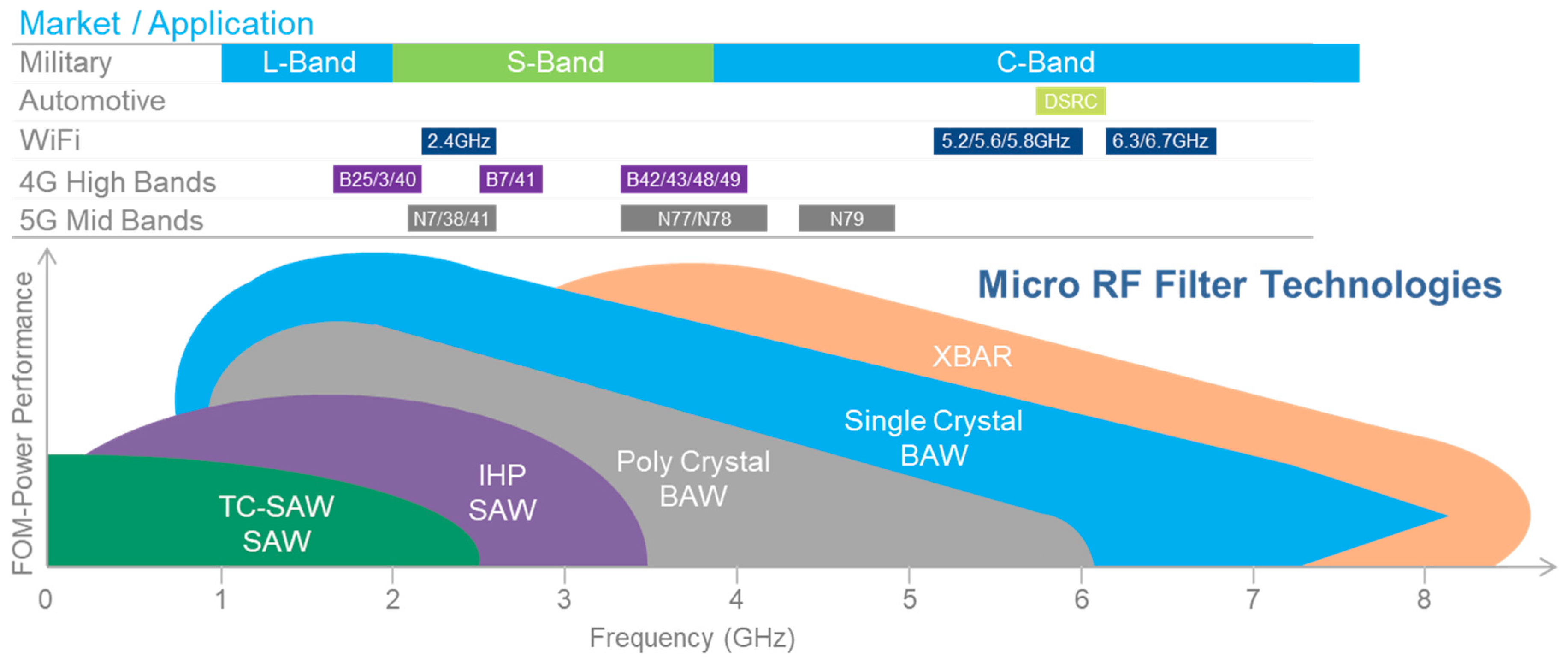
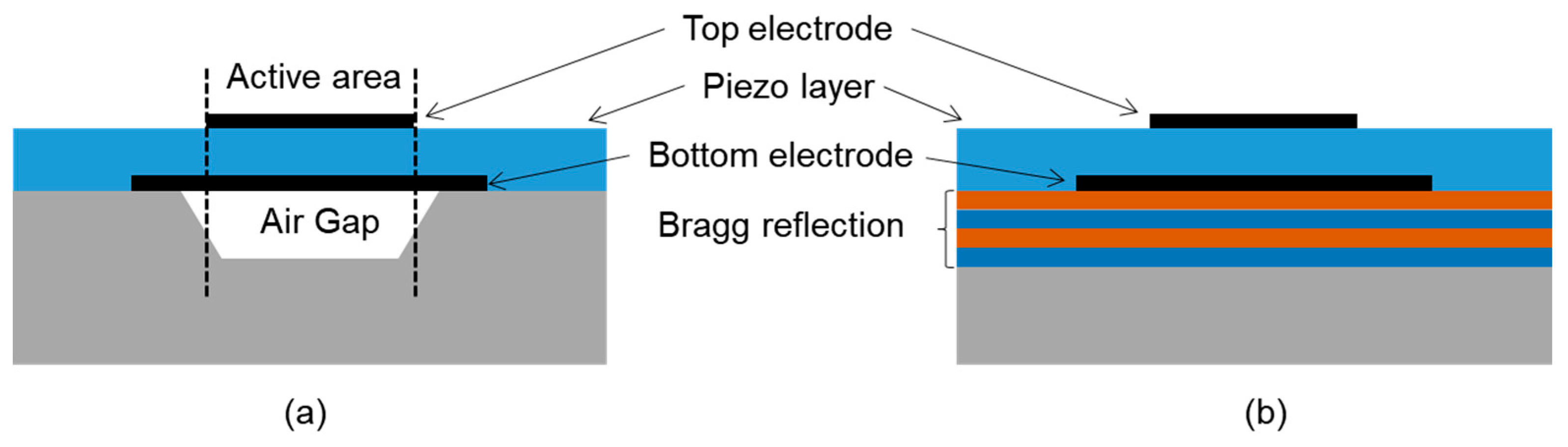
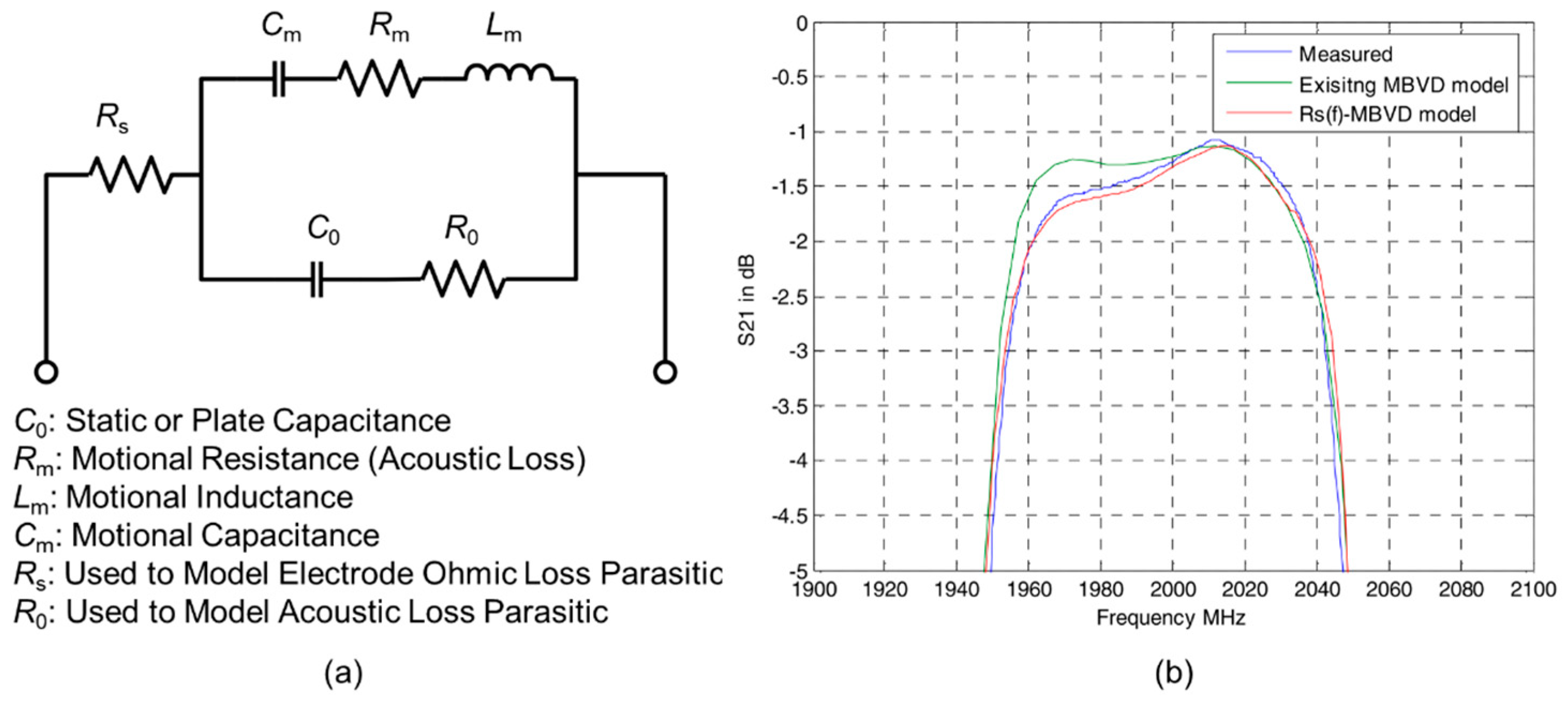
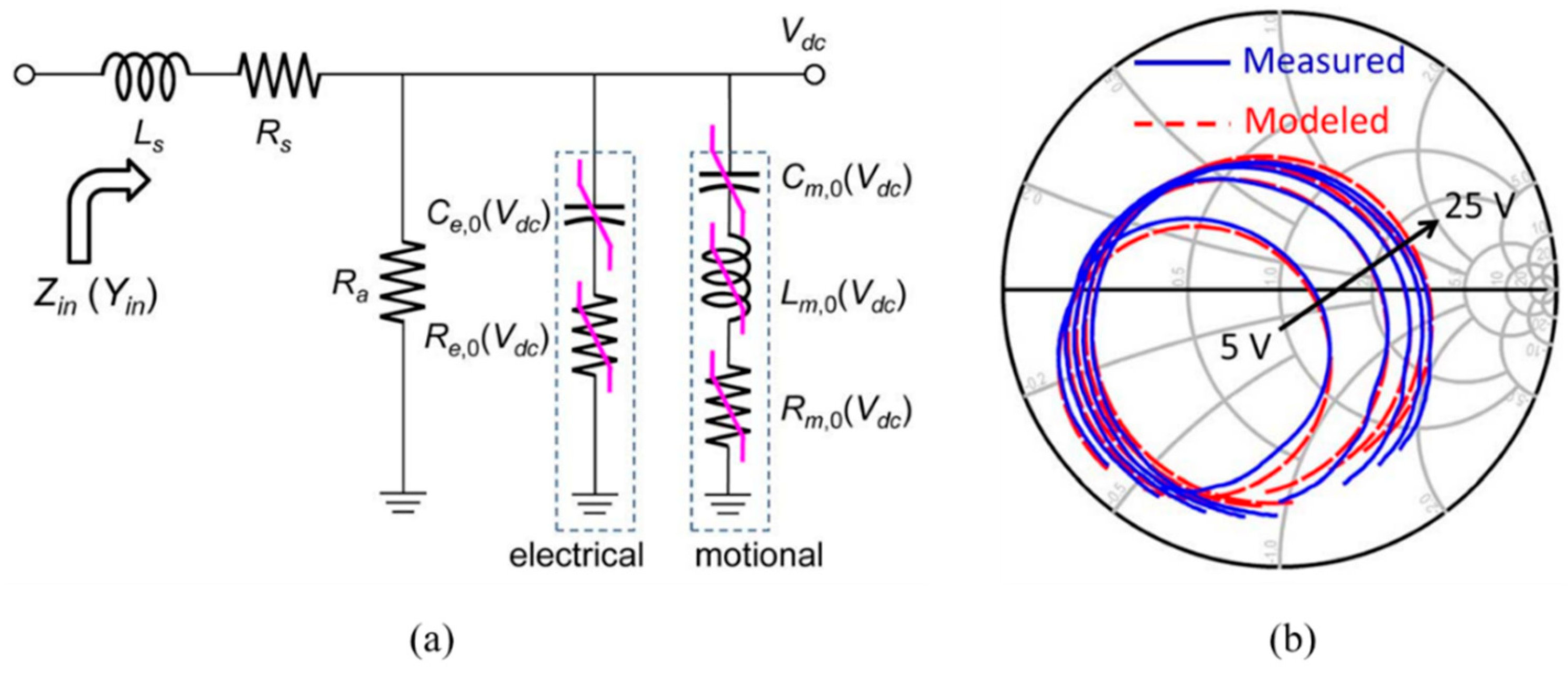
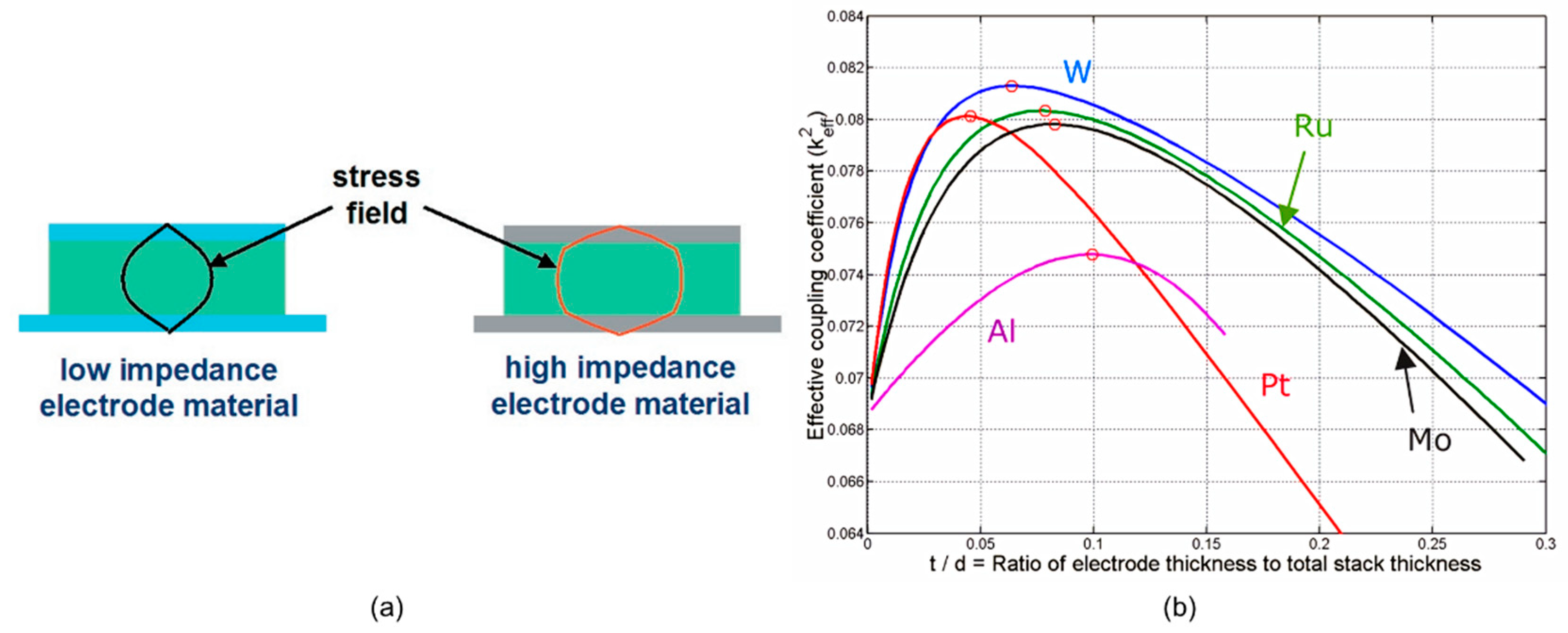
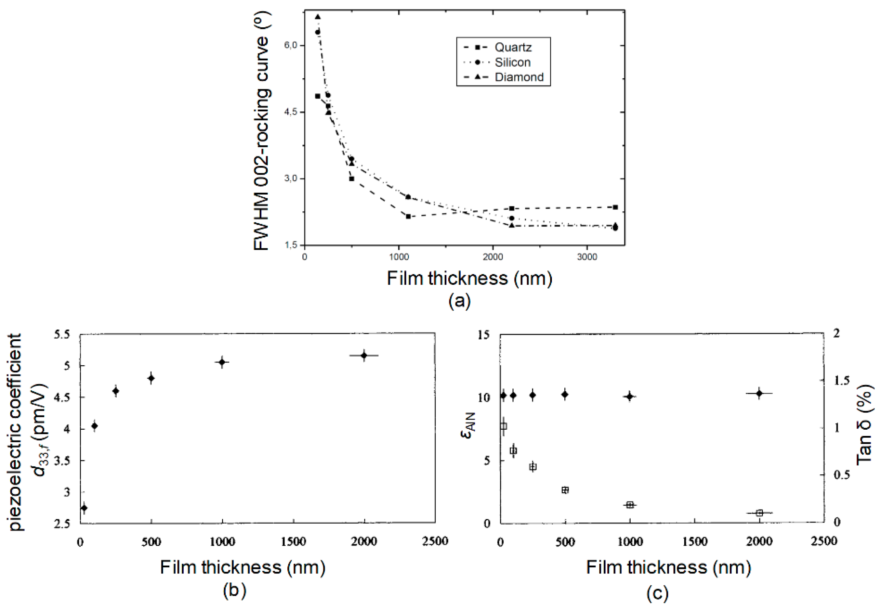
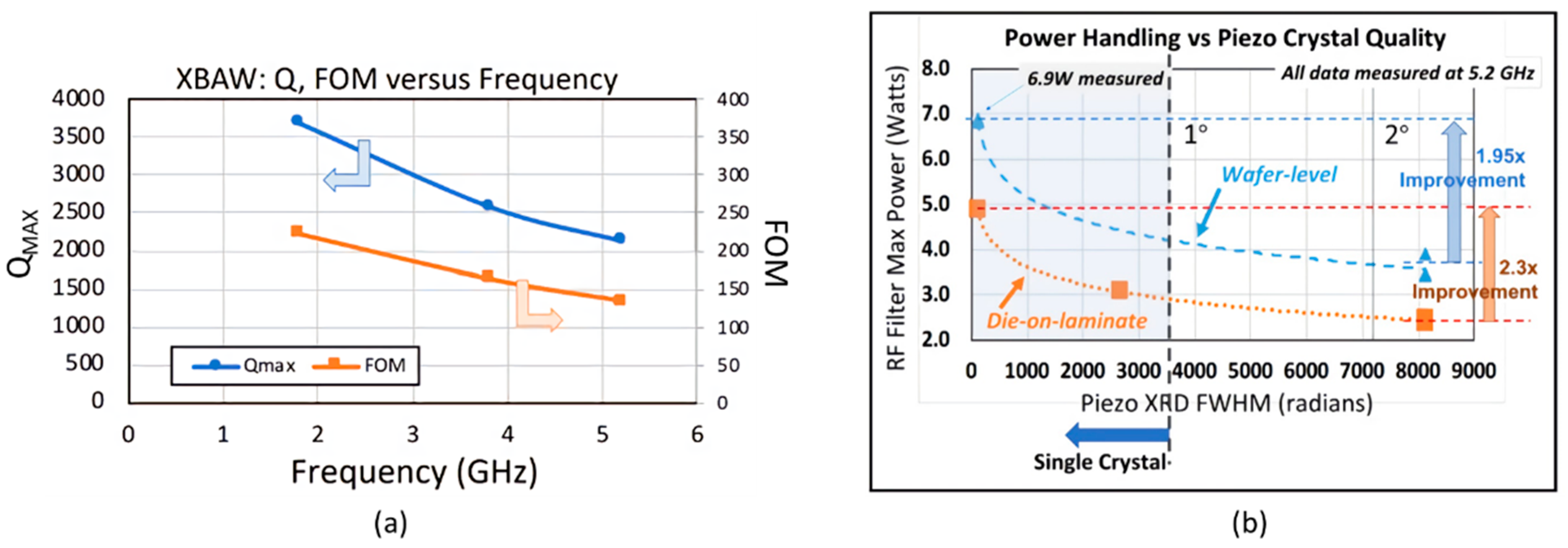
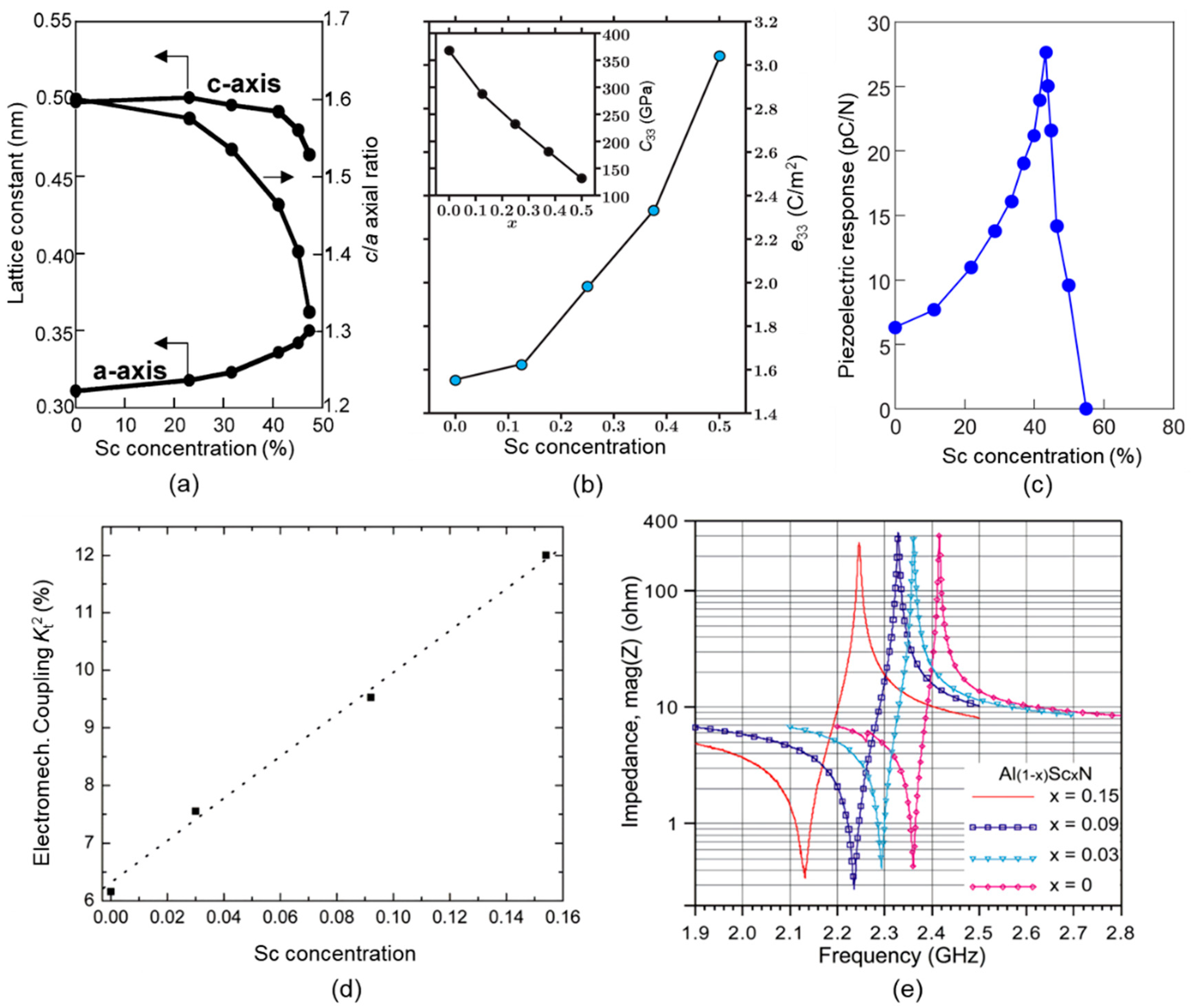
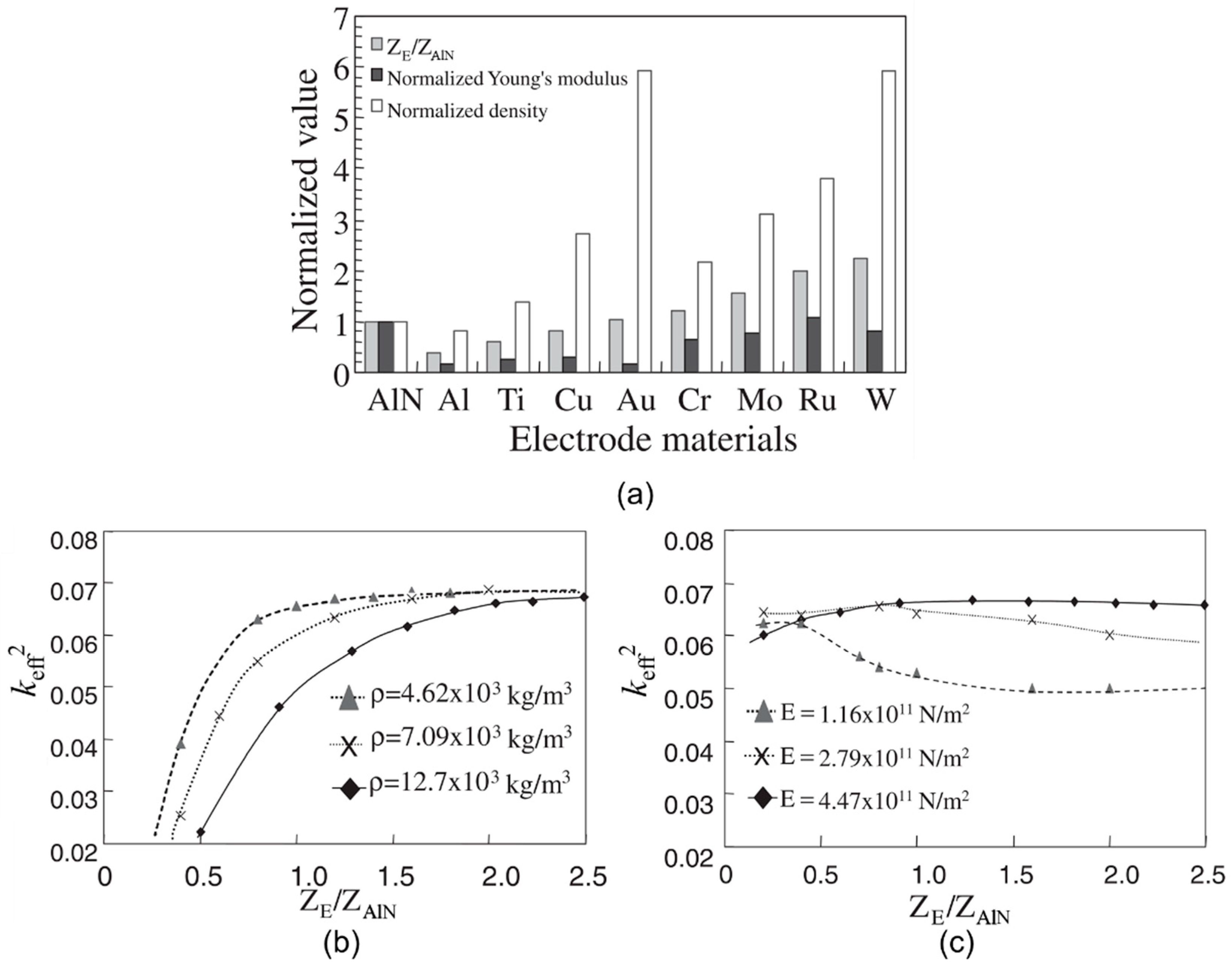
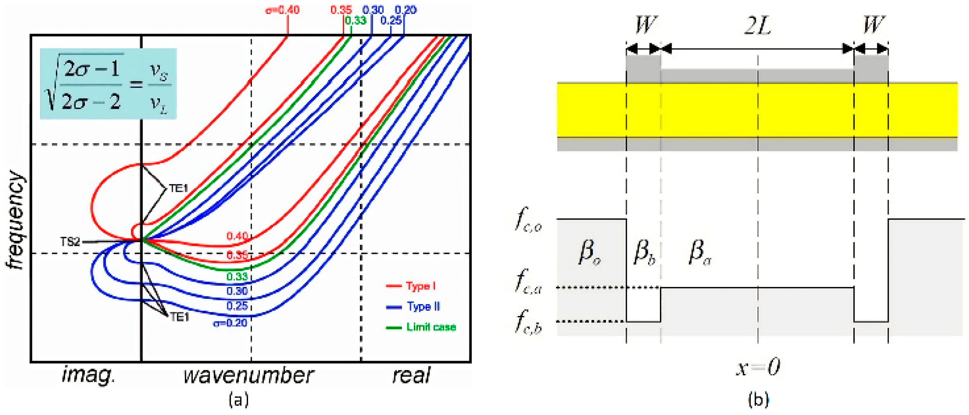
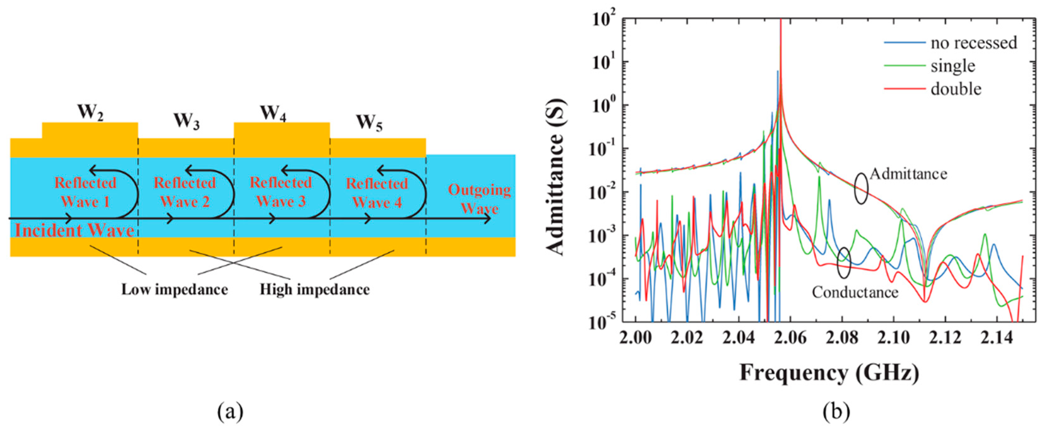
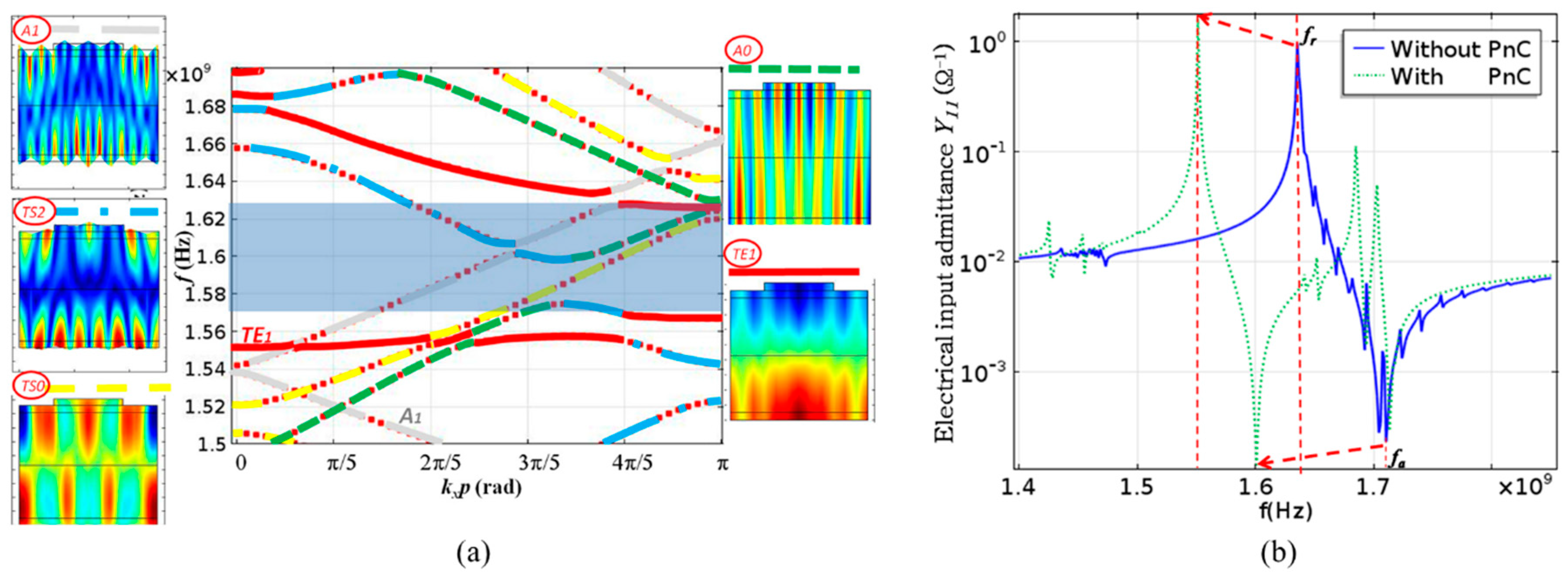
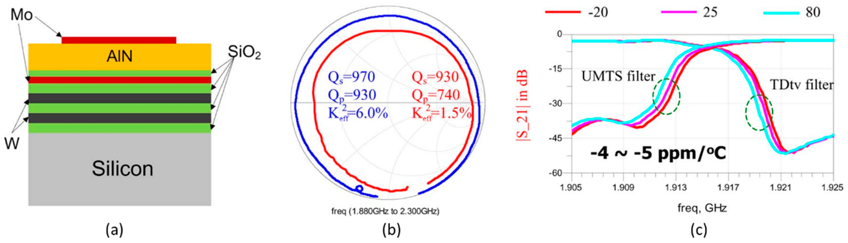
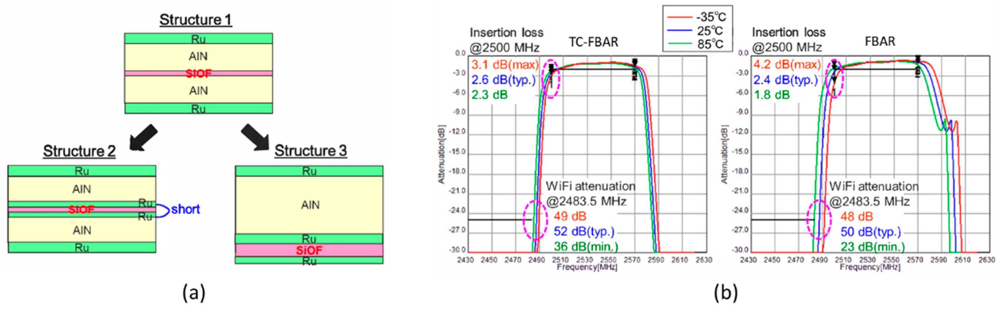
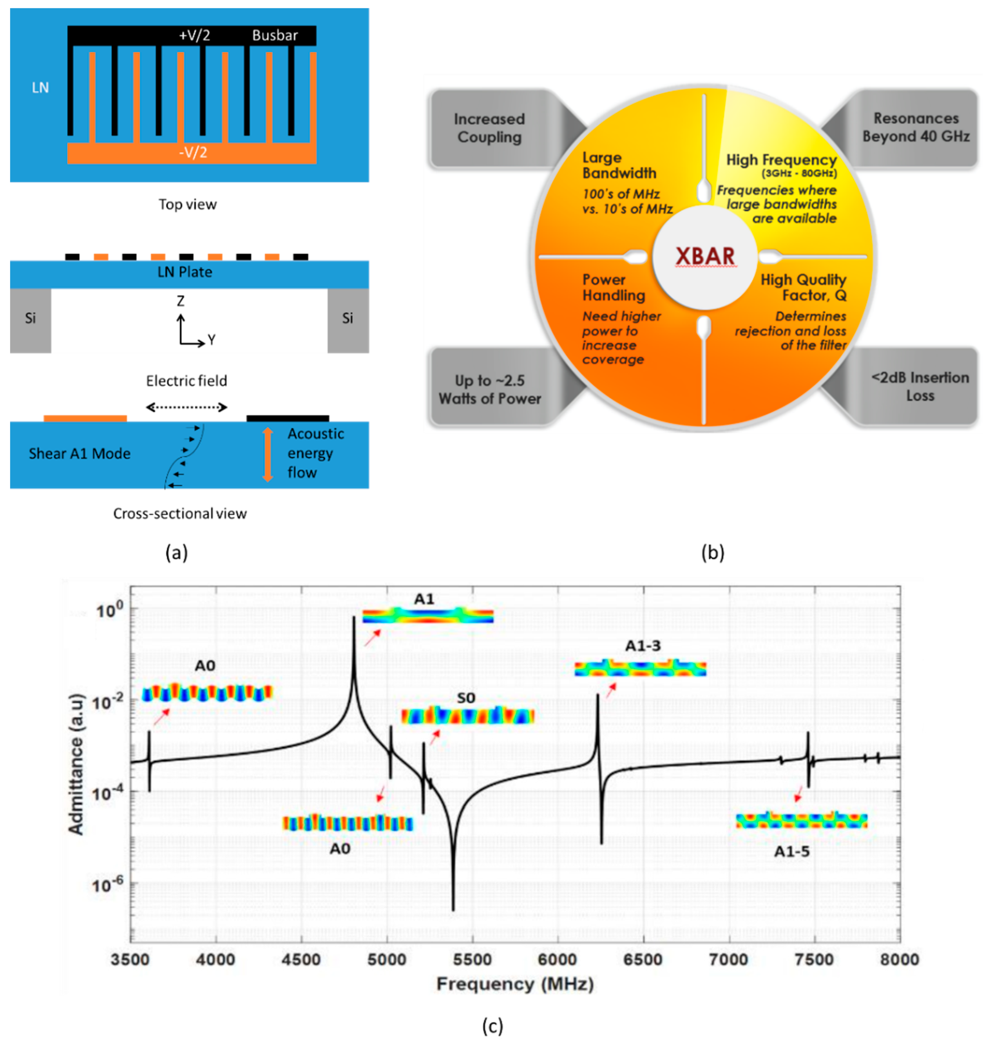
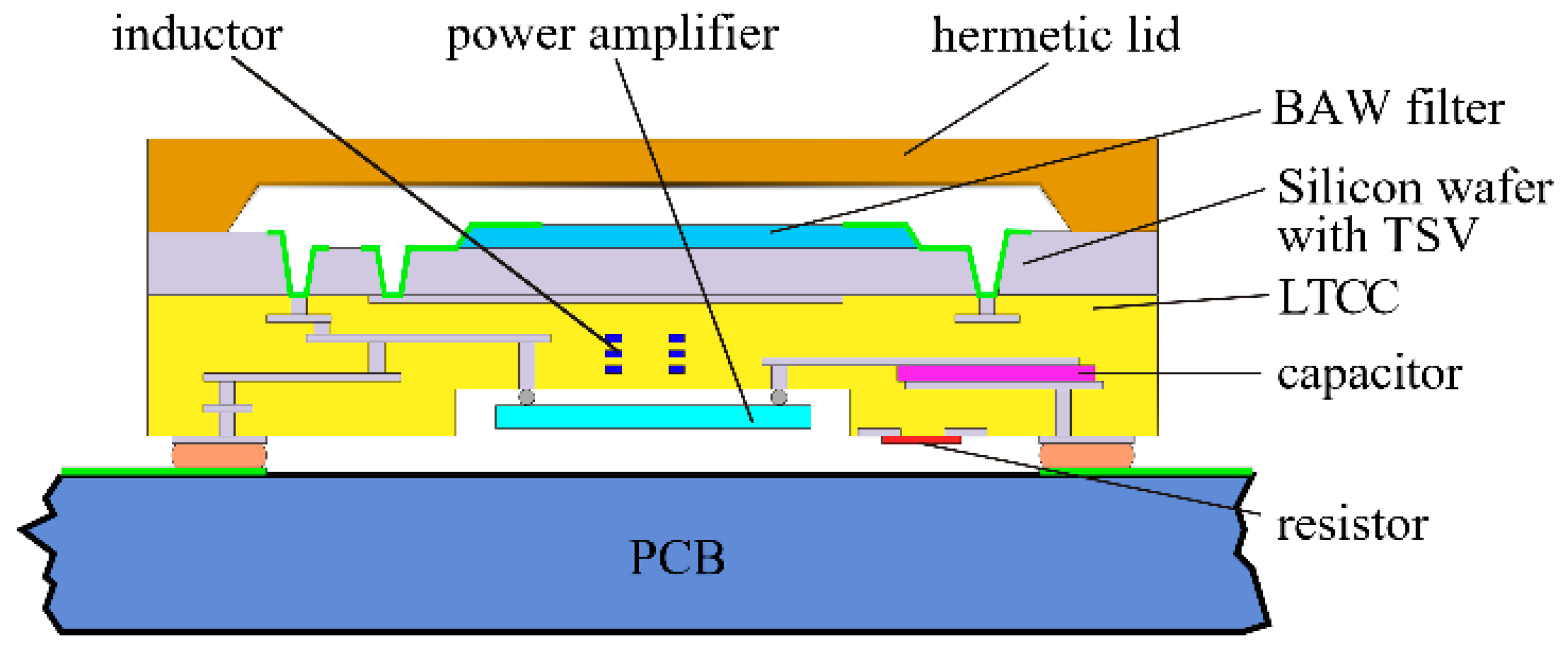
Table 1.
Crystal structure types of different metals (F: face-center cube; B: body-center cube; and H: close row hexagon) [55,57,60].
| Metal | Au | Pt | Al | Ag | Cu | Ir | Mo | Cr | Nb | W | Fe | Ru | Ti | Co | Zn | Zr |
|---|---|---|---|---|---|---|---|---|---|---|---|---|---|---|---|---|
| Crystal structure | F | F | F | F | F | F | B | B | B | B | B | H | H | H | H | H |
Table 2.
The Poisson’s ratio of different materials. Data from [85].
Table 2.
The Poisson’s ratio of different materials. Data from [85].
| Material | Al | W | MO | AlN | SiO2 | Si3N4 | Si | ZnO |
|---|---|---|---|---|---|---|---|---|
| σ | 0.34 | 0.29 | 0.30 | 0.25 | 0.17 | 0.28 | 0.22 | 0.39 |
Table 3.
Impact of adding capacitors and inductors to BAW resonators.
| Series C | Parallel L | Parallel C | Series L |
|---|---|---|---|
| when C ↑ | when L ↑ | when C ↑ | when L ↑ |
| fs → fp fp does not change | fp ↑ fs does not change | fs ← fp fs does not change | fs ↓ fp does not change |
Table 4.
Performance of reported BAW resonators based on tunable materials.
| Material | Freq (GHz) | Tuning Ability1 (%) | Max Bias (V) | Q2 | Max keff2 (%) | Reference |
|---|---|---|---|---|---|---|
| SrTiO3 | 5.87 | fr:1 | 7.5 | 78(Qs) | 2 | [110] |
| BaTiO3 | ~4 | fr:1.3 fa:4.0 | 10 | 30 | 6.2 | [108] |
| Ba0.25Sr0.75TiO3 | ~4 | fr:1.2 fa:0.8 | 10 | 120 | 0.5 | [108] |
| Ba0.25Sr0.75TiO3 | ~5 | fr:0.9 | 25 | 250(Qs) 350(Qs-de) | – | [111] |
| Ba0.25Sr0.75TiO3 | 5.46 | fr:2 | 50 | 50(Qs) 140(Qp) | 4.4 | [112] |
| Ba0.25Sr0.75TiO3 | 5.76 | fr:3.8 | 25 | 130(Qs) | 7.1 | [113] |
| Ba0.25Sr0.75TiO3 | 5.46 | fr:1.9 | 50 | 260(Qs-de) | 3.5 | [114] |
| Ba0.3Sr0.7TiO3 | 2.85 | fr:2.4 fa:0.6 | 615 kV/cm | 200(Qs) 120(Qp) | 4.4 | [109] |
| Ba0.5Sr0.5TiO3 | 5.45 | fr:2.4 | 50 | 250(Qs-de) | 7.5 | [114] |
| Ba0.7Sr0.3TiO3 | 5.44 | fr:1.3 | 6 | 352.6(Qs) 746(Qp) | 17.15 | [115] |
1 Tuning ability at resonance frequency fr and antiresonance frequency fa. 2 Q-factor at series resonance Qs, parallel resonance Qp and series resonance after de-embedding Qs-de.
© 2020 by the authors. Licensee MDPI, Basel, Switzerland. This article is an open access article distributed under the terms and conditions of the Creative Commons Attribution (CC BY) license (http://creativecommons.org/licenses/by/4.0/).
Share and Cite
MDPI and ACS Style
Liu, Y.; Cai, Y.; Zhang, Y.; Tovstopyat, A.; Liu, S.; Sun, C. Materials, Design, and Characteristics of Bulk Acoustic Wave Resonator: A Review. Micromachines 2020, 11, 630. https://doi.org/10.3390/mi11070630
AMA Style
Liu Y, Cai Y, Zhang Y, Tovstopyat A, Liu S, Sun C. Materials, Design, and Characteristics of Bulk Acoustic Wave Resonator: A Review. Micromachines. 2020; 11(7):630. https://doi.org/10.3390/mi11070630
Chicago/Turabian StyleLiu, Yan, Yao Cai, Yi Zhang, Alexander Tovstopyat, Sheng Liu, and Chengliang Sun. 2020. "Materials, Design, and Characteristics of Bulk Acoustic Wave Resonator: A Review" Micromachines 11, no. 7: 630. https://doi.org/10.3390/mi11070630
Note that from the first issue of 2016, this journal uses article numbers instead of page numbers. See further details here.