
Abstract
Laser micro-structuring of amorphous polyether(ether)ketone (PEEK) has been demonstrated with 180 fs/1 kHz NIR (775 nm) and NUV (387 nm) laser pulses. Significant differences in laser-material interaction is observed between the NIR and NUV wavelengths with single pulse ablation threshold found to be 2.01 ± 0.05 J cm−2 and 0.23 ± 0.02 J cm−2 at 775 nm and 387 nm respectively. This is connected to the requirement for multi-photon absorption at 775 nm, where PEEK is transparent, while at 387 nm, significant linear absorption within the material bandgap occurs, favouring sequential 2-photon absorption via reverse saturated absorption (RSA). Open aperture Z scan data yields a 2-photon absorption coefficient β387(I) which is intensity dependent, consistent with RSA. Multi-pulse exposure yields incubation coefficients of S775 = 0.72 ± 0.01 and S387 = 0.85 ± 0.02. This significant reduction in NUV incubation is consistent with a much higher level of electron excitation to the conduction band. Consequently, ablation of PEEK with NUV fs pulses is superior, exhibiting much reduced melting and re-deposition. Precision NUV polymer surface micro-structuring is accomplished while laser induced periodic surface structures (LIPSS) with pitch Λ ∼ 0.4 μm are observed at the base of ablated regions, aligned parallel to the incident polarisation. The ease of NUV LIPSS generation allowed surface patterning of large scanned areas which exhibit white light diffraction due to this sub-micron periodic surface modulation.
Export citation and abstract BibTeX RIS

Original content from this work may be used under the terms of the Creative Commons Attribution 4.0 license. Any further distribution of this work must maintain attribution to the author(s) and the title of the work, journal citation and DOI.
1. Introduction
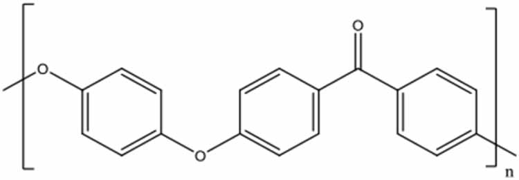
Laser structuring of soft matter such as polymers is relevant to current applications in nano-electronics, solar cells and medical implants. Polyether ether ketone (PEEK) is a high performance thermoplastic polymer with outstanding mechanical and chemical properties, high temperature resistance and good biocompatibility. PEEK is therefore an ideal candidate for applications in electronics, medicine and surgery, aerospace and automotive [1, 2]. PEEK coatings also exhibit an excellent tribological performance with a relatively low coefficient of friction and wear rate [3]. Amorphous PEEK can be used in aerospace insulation, acoustic speaker diaphragms, electrical insulation and potentially a metalised film capacitor dielectric, with a high breakdown strength E > 100 MV m−1 [4]. Its chemical structure is shown in figure 1.
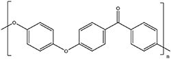
Figure 1. Chemical structure of PEEK.
Download figure:
Standard image High-resolution imagePhoto-etching or cold ablation of organic polymers was first addressed with nanosecond, excimer UV laser pulses where the photon energy is close to or exceeds the molecular bond energies [5–7]. However, in Teflon at 248 nm and PMMA at 308 nm, where linear absorption is low, these suffered severe surface degradation while exposure to ultrahigh intensity pulses resulted in clean ablation with good edge quality, mediated by multi-photon absorption [8, 9]. The advantage of using ultrafast laser pulses combined with shorter UV wavelengths was therefore early appreciated. With the introduction of NIR ultrafast Ti-sapphire amplifier systems, micro-structuring of transparent polymers with ultrahigh intensities followed [10–12] with excellent results on polyimide and appreciation of the role of incubation. Femtosecond processing of PEEK with visible, 595 nm pulses was first demonstrated by Serafetinides et al [13] and reported sub-micron periodic structures which they attributed to relaxation of unidirectional laser induced stress on the polymer surface.
More recently, comparison of the excimer (248 nm) and femtosecond (800 nm/100 fs) laser ablation of thermoplastic material, acrylonitrile butadiene styrene showed that ablation threshold and changes in surface chemistry are dependent on the wavelength as well as pulse length [14]. Other processing methods also include chemical etching and plasma treatments, however, aromaticity within the polymer backbone may offset the etching in the latter [15]. Chemical etching may also damage the surface layer [16].
Precision surface texturing on PEEK for improved wear resistance was recently demonstrated using femtosecond (130 fs/800 nm/5 kHz) laser pulses as well as generating sub-micron periodic surface structures (LIPSS) on both semi-crystalline and amorphous PEEK [17, 18]. The window for LIPSS generation at 800 nm was, however very narrow. LIPSS were also generated on poly-L-lactic acid (PLLA) with 800 nm and 400 nm/100 fs pulses [19] with a much wider structuring window at 400 nm. Femtosecond laser induced LIPSS on thin polymer films of PET, PTT and PC using 265 nm and 795 nm were generated with fluence well below ablation threshold combined with high pulse numbers [20, 21]. The fundamentals of LIPSS generation on polymer films have been considered and in the case of amorphous polymers, the surface temperature during exposure should exceed the glass transition temperature Tg [22].
The aim of the present study is to elucidate the laser-material interactions by comparing the ablation threshold, incubation effect and the optical properties of amorphous PEEK at 775 nm and 387 nm with fs pulse excitation. The use of the thin film transparent amorphous PEEK allows the measurement of the optical properties, impossible with standard semi-crystalline material which is opaque. While the measured linear absorption coefficient at 775 nm is negligible, it is significant in the NUV at 387 nm, just within the polymer bandgap. Non-linear absorption was also detected in the NUV above peak intensity I > 1 GW cm−2 indicating a high 2-photon (2 PA) absorption coefficient. The clear advantage of using NUV fs pulses over NIR allows precision 3D PEEK micro-structuring with no evidence of polymer melting so that large area sub-micron LIPSS patterning was achieved.
2. Experimental
2.1. Experimental set-up
The experimental system has been described in detail previously [23]. A Titanium-sapphire laser system (Clark-MXR CPA 2010) provides a pulse energy of 1 mJ at 1 kHz with pulse duration of 180 fs at 775 nm (M2 ∼ 1.3). The beam was split into two lines, NIR and NUV enabled by an ultrafast thin film beam splitter. In the 775 nm line, the reflected beam passed through a fast shutter, attenuated, then expanded × 3 in a Galilean telescope and directed to a Galvo scanner with flat field lens (Nutfield XLR8 scan head with 100 mm f-theta lens). The sample was set perpendicular to the laser beam on a micro position translation stage (Aerotech, x, y, z, θ).
In the second beam line, the transmitted component at 775 nm was frequency-doubled to generate the 387 nm NUV wavelength in a thin, 0.6 mm thick beta barium borate (BBO) crystal and focussed by a 100 mm focal length lens for micro-machining PEEK substrates, supported by an Aerotech ATS115 stage (x,y,z). All treatments were conducted in air at atmospheric pressure.
2.2. Materials
The substrate used was amorphous PEEK (25, 50, 75, 100 and 200 µm thick, Goodfellow) This material is optically transparent with surface flatness Ra < 0.2 µm, however, the 100 and 200 µm thick films required optical polishing using aluminium oxide polishing films with 3 µm, 1 µm and 0.3 µm grit size (Thorlabs). Prior to experiments, the PEEK samples were cleaned in methanol with an ultrasonic treatment for 5 min.
2.3. Surface characterization
An optical microscope (Nikon) was used to observe the machined features and a white light interferometer (WYKO NT1100) measured the depth and cross sections of each spot. All data was measured five times and then an average taken. The detailed surface morphology was observed by a scanning electron microscope (JSM-6610 SEM and ZEISS Sigma). Raman spectra of micro-structured surfaces were also observed using a Raman microscope with the 325 nm laser line of a Horiba JY Labram HR system. Material micro-structure was measured using XRD (Rigaku MiniFlex).
3. Experimental results
3.1. Crystallinity of material
Bulk PEEK can have a significant semi-crystalline structure and commercial PEEK is often opaque. The thin (transparent) films used here were supplied as 'amorphous' hence we checked the micro-structure using XRD (Rigaku MiniFlex). Figure 2 shows the XRD spectrum of the 100 µm and 200 µm amorphous PEEK films and compared to XRD of bulk semi-crystalline PEEK. The difference is highly significant. In the amorphous films, there are no sharp peaks, characteristic of a semi-crystalline phase but only a broad feature which is due to x-ray fluorescence. On the other hand, the commercial, opaque sample exhibits four intense, sharp diffraction peaks with a number of low intensity features at higher angles. The films used here are therefore mainly amorphous. If a semi-crystalline component exists, then it is at the few % level [17].

Figure 2. XRD spectra of amorphous and bulk, semi-crystalline PEEK.
Download figure:
Standard image High-resolution image3.2. Morphological results
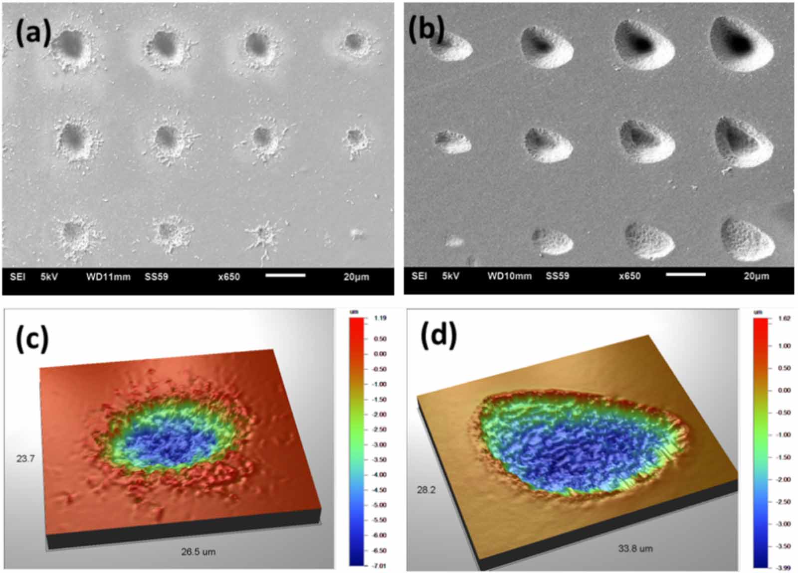
The ablated spots on the amorphous PEEK surface with 20, 50 and 100 pulses and a range of pulse energies at 775 nm and 387 nm are shown in figure 3. The laser beam spot sizes were estimated to be 15 µm and 34 µm at the focus for 775 nm and 387 nm respectively (from the gradients of figure 5). Samples were set normal to the incoming laser beams. The machined spot sizes increase with both laser fluence and pulse number as expected. Significant re-deposition and evidence of melting appear around the spots at 775 nm with ejected material radiating from the centre. Interestingly, at lowest fluence and exposure, the material did not ablate but expanded to a small bump on the surface, figure 3(a), bottom right. Such behaviour has been previously reported due to sub surface material breakdown from incubation centres causing de-composition and swelling [11]. On the contrary, femtosecond ablation of PEEK at 387 nm is superior with almost no material re-deposition and little evidence of melt, figure 3(b). This infers a significant change in the laser-material interaction from NIR to NUV with photon energies of 1.6 eV and 3.2 eV respectively. Figures 3((c) and (d)) show 3D surface profiles (WYKO) of ablation spots treated by NIR and NUV exposure. The NUV craters were more elliptical in shape.

Figure 3. (a) SEM micrograph image of ablation spots on PEEK at 775 nm with 100 mm f-theta lens. From right to left: fluence F = 0.94, 1.21, 1.48, 1.75 J cm−2, from top to bottom: 100, 50, 20 pulses, (b) SEM micrograph image of ablation spots at 387 nm with objective focal length f = 100 mm. From left to right: fluence F = 0.18, 0.26, 0.36, 0.44 J cm−2, from top to bottom: 100, 50, 20 pulses. (c) 3D display of ablated crater with fluence F = 1.75 Jcm−2, 20 pulses at 775 nm. (d) 3D display of ablated crater with fluence F = 0.18 Jcm−2, 50 pulses at 387 nm.
Download figure:
Standard image High-resolution imageAt the NUV wavelength, Laser-Induced Periodic Surface Structures (LIPSS) were observed on the base of the ablated PEEK craters parallel to the incident linear polarisation. Figures 4((a) and (b)) shows SEM imaging of these low spatial frequency LIPSS structures (LSPL) at fluence F = 0.36 J cm−2 with N = 20 and N = 50 respectively. At N = 50, the pitch near the crater centre is Λ ∼ 0.5 μm reducing at the crater edge to Λ ∼ 0.33 μm where the laser exposure is less.

Figure 4. (a) SEM micrograph image of ablation spot at 387 nm, F = 0.36 J cm−2, N = 20 pulses showing LIPSS at the base with period ∼ 0.5 μm. (b) SEM micrograph image of ablation spot at 387 nm, F = 0.36 J cm−2, N = 50 pulses showing very clear LIPSS (LSPL). The fringe period near the centre (where intensity was highest) is approximately Λ1 ∼ 0.5 μm while at the edge on the walls, the period is significantly lower, Λ2 ∼ 0.33 μm where the exposure is reduced.
Download figure:
Standard image High-resolution image3.3. Ablation threshold
The ablation threshold was measured at both wavelengths which helps to clarify the laser-material interaction and the efficiency of ultrashort laser coupling to the material. The experiment was performed with single pulse, 20, 50 and 100 pulses at a range of pulse energies.
For a Gaussian beam, using the standard approach, the squared diameters of the ablated area D2 are directly related to the fluence by [11]
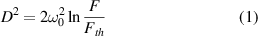
where D is the diameter of the spot ablated on PEEK, and Fth is the ablation threshold of the material. Figure 5 shows plots of D2 versus Ln F obtained for both 775 nm and 387 nm for single and multi-pulses highlighting that incubation is relevant. The slopes yield the effective beam diameters of 15 μm (775 nm) and 34 μm (387 nm) respectively. Measured fluence thresholds are summarised in table 1.
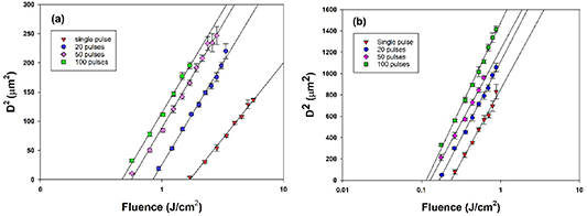
Figure 5. D2 curves versus fluence for 1, 20, 50 and 100 pulses at (a) 775 nm, (b) 387 nm.
Download figure:
Standard image High-resolution imageTable 1. Ablation threshold values, Fth at 775 nm and 387 nm for different number of pulses per spot N.
| N |  |
 |
|---|---|---|
| 1 | 2.01 ± 0.05 | 0.23 ± 0.02 |
| 20 | 0.84 ± 0.01 | 0.16 ± 0.01 |
| 50 | 0.66 ± 0.01 | 0.13 ± 0.01 |
| 100 | 0.55 ± 0.01 | 0.11 ± 0.01 |
There is a significant reduction in the ablation thresholds at λ = 387 nm compared to λ = 775 nm. Single pulse threshold is almost an order of magnitude lower at 387 nm and still a factor of 5 lower at N = 100 pulses inferring a much higher coupling efficiency to PEEK in the NUV.
3.4. Incubation coefficient
According to the incubation model proposed by Jee [24], the ablation threshold fluence Fth(N) for N pulse number and the single pulse ablation threshold Fth(1) are related by Fth(N) = Fth(1) × NS−1 where S is the incubation coefficient and Fth (1) is the ablation threshold for N = 1.
The equation can be expressed in the following form:

The proportionality coefficient S characterises the degree of accumulation in the material. Figure 6 shows plots of equation (2) for both 775 nm and 387 nm with solid lines representing a least square fit to the equation. The incubation coefficient S obtained from the slope of the line yields S775 = 0.72 ± 0.01 and S387 = 0.85 ± 0.02 respectively hence incubation at 775 nm is more significant than at 387 nm on PEEK using femtosecond laser excitation. Incubation proceeds by photochemical reactions that accumulate defects which act as absorbing sites hence the resulting ablation is more thermal in nature [25, 26]. This is significantly reduced at 387 nm where the incubation coefficient is similar to that of some metals, e.g. S = 0.86, 0.83, 0.87 for stainless steel, titanium and copper respectively [27].

Figure 6. Plot of Ln (N × Fth) versus pulse number N for amorphous PEEK at 775 nm and 387 nm yielding linear plots. The gradients give the incubation coefficients S775 = 0.72 ± 0.01 and S387 = 0.85 ± 0.02 respectively. The high value for 387 nm is similar to a range of metals.
Download figure:
Standard image High-resolution image3.5. Ablation rate
The ablation depth per pulse,  , is given for a wide range of materials and pulse lengths by [28],
where α is the absorption coefficient of the material at the laser wavelength,  is applied laser fluence and
  is the single pulse ablation threshold of the material.
Figure 7 presents the observed ablation rate per pulse with incident fluence and pulse number. From figure 7, the optical penetration depths (d ∼ α−1) and corresponding effective absorption coefficients of amorphous PEEK at the two wavelengths are summarized in tables 2 and 3 respectively. These remarkably small optical penetration depths confirm that there is strong multi-photon absorption involved. At 775 nm, the effective absorption coefficient increases with exposure while at 387 nm, absorption is almost independent of pulse number. This is consistent with the lower level of incubation.
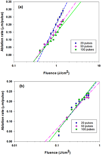
Figure 7. Ablation rate per pulse versus fluence at (a) 775 and (b) 387 nm.
Download figure:
Standard image High-resolution imageTable 2. The optical penetration depth d = α−1 (nm) at 775 nm and 387 nm with pulse number.
| 20 pulses | 50 pulses | 100 pulses | |
|---|---|---|---|
| 775 nm | 229 | 169 | 153 |
| 387 nm | 113 | 104 | 116 |
Table 3. The effective absorption coefficient α (cm−1) at 775 nm and 387 nm with pulse number.
| 20 pulses | 50 pulses | 100 pulses | |
|---|---|---|---|
| 775 nm | 4.4 104 104 |
5.9 104 104 |
6.5 104 104 |
| 387 nm | 8.9 104 104 |
9.7 104 104 |
8.6 104 104 |
3.6. Optical properties of amorphous PEEK
3.6.1. Linear absorption.
The optical transmission of amorphous PEEK films was measured in a spectro-photometer (SPECORD 250) and results are shown in figure 8(a). The cut off wavelength is around λ ∼ 390 nm. Thus, amorphous PEEK is highly transparent at 775 nm while linear absorption occurs at 387 nm, within the band edge.

Figure 8. (a) Transmission of amorphous PEEK with wavelength, (b) measured linear transmission at 775 nm and 387 nm with film thickness and for comparison, at 400 nm (low intensity I < 200 MW cm−2). The solid curves at 387 and 400 nm are exponential fits, yielding α0(387) = 300 cm−1 and α0(400) = 88 cm−1 respectively.
Download figure:
Standard image High-resolution imageFigure 8(b) shows the measured transmission versus film thickness with collimated low intensity laser beams at 775 nm, 387 nm and for comparison, at 400 nm just on the band edge. Here, a femtosecond laser source (Coherent Libra, 800 nm, 120 fs) was frequency doubled in BBO for these measurements. Light will be attenuated when passing through the material according to the Beer–lambert Law. Allowing for reflection losses, this gives transmission,

where α0 (λ) is the linear absorption coefficient (cm−1), z is the material thickness (cm) and R is the surface reflectivity of PEEK in air. As  [25], then
  from the Fresnel equation [29]. In a transparent region, the expected transmission is then
  and confirmed above at 775 nm. From figure 8(b), we estimate a weak linear absorption coefficient α0 (775) ∼ 6.4 cm−1 while at 387 nm within the band edge, the exponential drop in transmission with film thickness corresponds to a linear absorption coefficient α0(387) = 300 cm−1. The linear absorption coefficient at 400 nm, α0(400) = 88 cm−1 highlights the sensitivity of absorption to wavelength in this band edge region. Peak intensity I < 200 MW cm−2 here.
3.6.2. Nonlinear absorption.
When transmission becomes intensity dependent, this is evidence of a non-linear response. Measured transmission with peak intensity and film thickness is shown in figures 9(a)–(c). At 775 nm, the transmission of PEEK is independent of incident peak intensities up to 6 GW cm−2. On the other hand, transmission at 387 nm changes significantly at incident intensities above 1 GW cm−2, indicating non-linear 2-photon absorption. The cut offs on the vertical axis reflect the linear absorption with film thickness. At longer NUV wavelength, 400 nm, figure 9(c), a weak non-linear absorption is just detectable on the band edge.
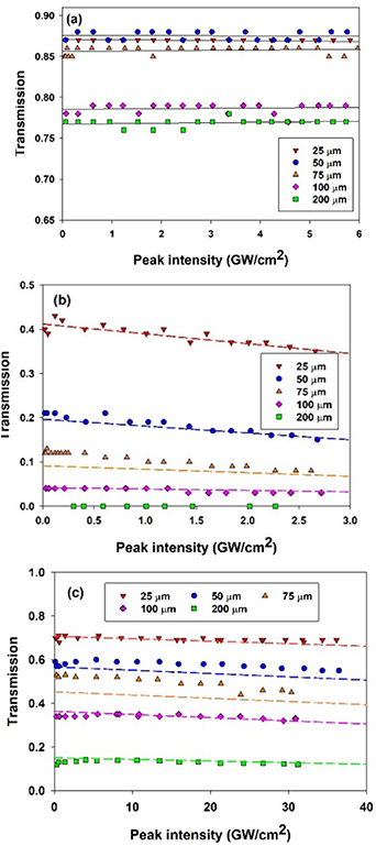
Figure 9. Transmission in PEEK films as a function of incident peak intensity at (a) 775 nm, (b) 387 nm, (c) 400 nm for various sample thicknesses. Non-linear absorption at 387 nm is consistent with β(387) ∼ 38 cm GW−1, reducing significantly at 400 nm to β(400) ∼ 0.7 cm GW−1. The dashed lines in (b) and (c) represent the theoretical fits to equation (6) with linear absorption coefficients α0(387) = 300 cm−1 and α0(400) = 88 cm−1 calculated from equation (4) and data of figure 8(b).
Download figure:
Standard image High-resolution imageWhen both linear and non-linear 2-photon absorption occur simultaneously in a material, the rate of change of intensity is given by,
where α0 is the linear absorption coefficient and β is the 2-photon absorption coefficient. The total absorption coefficient is then α = α0 + βI. Integration yields the transmission T [30],
From figure 9(b), we can estimate the non-linear 2-photon absorption coefficient for amorphous PEEK at 387 nm using the measured α0(387) = 300 cm−1 while adjusting β to give the best fit to equation (6). Setting β(387) = 37.8 cm GW−1, the fits to the data are excellent apart from the 75 μm film whose linear absorption appeared slightly high. At 400 nm, on the very edge of the bandgap, much higher intensities were required to detect non-linear absorption, figure 9(c) where reasonable fits to β(400) = 0.7 cm GW−1 are obtained with some variation, particularly on the 75 μm film.
The measured value of β(387) is high for a polymer, inferring also a high third order susceptibility, χ(3) but organics containing conjugated bonds have a high density of polarisable π-electrons (as in the benzene rings in PEEK). For example, using the Z-scan technique, polythiophene doped PMMA films demonstrated values of β > 30 cm GW−1 with β also dependent on intensity above 1 GW cm−2—indicating that sequential 2-photon absorption (2 PA) was the relevant mechanism where the excited state cross section well exceeds the ground state absorption cross section. This non-linear process is termed reverse saturated absorption (RSA) [31].
In PEEK, as 387 nm has a photon energy within the bandgap, (3.15–3.29 eV) this high value of β(387) suggests that sequential 2-photon absorption via the real states populated in the conduction band by the first photon likely occurs with ultrahigh intensity fs excitation at 387 nm. This could be viewed as a resonance enhancement due to the proximity of these real states.
The film temperature (using FLIR camera),was measured to be ∼ 70 °C well below the glass transition temperature Tg = 143 °C [1] where structural changes could take place due to increased molecular mobility.
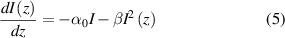
While our simple approach to measuring NL absorption yielded indicative results for β, nevertheless, a much more satisfactory approach uses the Z-scan technique [31]. The open-aperature Z scan was employed to investigate the nonlinear absorption of the 25 µm PEEK film at 387 nm while translating the sample through the focal plane of a long focal length lens ( f = 250 mm). Typical scans are shown in figure 10(a) with incident peak intensities of I0 = 78GWcm−2 and 160 GW cm−2 respectively with β adjusted to give the best fits to equation (7). The change in normalised intensity ΔT(z) as a result of two-photon absorption is given by [31–33].
Figure 10. (a) Open aperture Z scan data of amorphous 25 μm PEEK at I0 = 78 GW cm−2 and 160 GW cm−2 with best fits to β = 3.6 cm GW−1 and β = 4.0 cm GW−1 respectively. (b) Measured effective 2-photon absorption coefficient β versus peak intensity of 25 µm thick amorphous PEEK. This variation is consistent with RSA [32].
Download figure:
Standard image High-resolution imagewhere the free factor q0 = βI0Leff, where Leff = (1-e-αL)/α = 1.76 × 10⁻³ cm (α = 300 cm−1) and L = 2.5 × 10⁻³ cm is the sample thickness, I0 is the peak intensity at the beam focus (Z = 0) and Z0 is the Rayleigh range of the beam. With the 250 mm lens, the beam Rayleigh length was measured to be Z0 = 10.5 mm so that the sample thickness L ≪ Z0, required for this technique. The best fits in figure 10(a) yielded β = 3.6 cm GW−1 and β = 4.0 cm GW−1 at I0 = 78 GW cm−2 and 160 GW cm−2 respectively so that β becomes nearly constant at higher intensities. Figure 10(b) summarises the results of measured β with peak intensity showing that β is highly intensity dependent. As β = β(I) with β decreasing with intensity, this is strongly indicative of reverse saturation absorption [32, 34] whereas a constant β would be consistent with simultaneous 2-photon absorption. Pulse energies with E ≤ 1 μJ used during Z scans were measured with a Pyroelectric detector and averaged over 500 pulses.
During Z scan measurements, the FLIR SC660 camera was used to check temperature rise at the beam waist. The temperature rise observed—even with the highest exposure E = 1 μJ at 1 kHz (I0 ∼ 160GWcm−2, < P > = 1 mW) was < 2 °C, very satisfactory, figure 11(b). The beam profile at focus is also shown in figure 11(a), near Guassian with slight ellipticity.
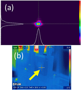
Figure 11. (a) NUV intensity profile at beam waist during Z scan showing nearly Gaussian profile. Beam waist diamater 2ω0 ∼ 96 μm. (b) Thermal image at beam waist with E = 1μJ/pulse (I0 ∼ 160 GW cm−2) corresponding to 2 °C temperature rise.
Download figure:
Standard image High-resolution imageWith a polymer density ρ = 1.3 g cm−3, molecular weight (EEK) = 288.3 and α0(387) = N0σ387 ∼ 300 cm−1, then the monomer molecular density n = 2.7 × 1021 cm−3 and corresponding single photon absorption cross section σ387 ∼ 1.1 × 10⁻¹⁹ cm2. Integrating β(I) with intensity,  dI in figure 10(b), we obtain an average 2-photon absorption coefficient ∼ 6.103 cm−1 ≫ α0 and 'effective' 2-photon cross section σeff ∼ < β387I >/N0 = 2.2 × 10⁻¹⁸ cm2 ≫ σ387 estimated above by an order of magnitude, supporting RSA.
From the ablation studies and optical measurements, non-linear 3-photon absorption (coupling 4.8 eV) is likely required to process the PEEK at 775 nm as the band gap is ∼ 3.2 eV, well above the photon energy, hν = 1.6 eV hence can proceed only through virtual transitions to the lowest  —dominated states in the conduction band (2 PA) followed by sequential photon absorption. This is consistent with the concept that charge-transfer excitons (e.g. states leading to dissociation) in conjugated polymers) are favoured by multiphoton processes [35]. On the other hand at 387 nm, single and sequential 2-photon absorption also occurs at 387 nm with 2-photons (6.4 eV) dominating this interaction at ultrahigh intensity I > 1012 W cm−2, figure 12. This diagram also shows the theoretically calculated density of states (DOS) for PEEK based on ab initio quantum calculations [4] so that a much higher density of states is available for the second photon 387 nm absorption and third photon at 775 nm. The major contribution to the DOS comes from the Carbon atoms. Transitions to the conduction band near 3.2 eV occur from the highest occupied levels in the valence band corresponding to degenerate e1 g electronic levels of benzene [36].

Figure 12. Band energy diagram (density of states) of PEEK and multi-photon absorption scheme. The density of states was calculated theoretically by Ho et al [4]. The major contribution to the DOS comes from carbon with much less from hydrogen and oxygen.
Download figure:
Standard image High-resolution imageA comparison of theoretical calculations of valence band electronic structure in PEEK with experimental results of UV photo-electron spectra yielded a bandgap Eb = 3.4 eV, a work function WF = 4.2 ± 0.2 eV and ionisation potential IP = 7.0 ± 0.2 eV [36]. Hence, three photon NIR and 2-photon NUV absorption can both generate direct photo-electron emission from the surface while further sequential photon absorption (3-photon) at 387 nm in the NUV via the high density of ( —dominated) states would couple 9.6 eV, able to photo-ionise the bulk material. This absorbed energy is able to break all the chemical bonds in PEEK directly, e.g. C–C (3.48 eV), C–O (3.73 eV), C = C (6.14 eV) and C–H (4.13 eV) and the C = O which has 8.28 eV. Hence polymer photo-dissociation and evaporation ('cold ablation') proceeds as the chemical bonds of the polymer are rapidly broken into molecular fragments or small particulates [37] with ejection of the plume of decomposed polymer debris [38].
3.6.3. Fluorescence spectrum of PEEK excited at λ = 387 nm.
The fluorescence spectrum of PEEK excited at 387 nm (low intensity) is shown in figure 13(a) measured with an Andor Shamrock SR-303i Spectrometer. This spectrum is very broad from 410 nm to 600 nm (peak λ ∼ 480 nm) showing a large Stokes shift inferring internal energy loss through rapid inelastic electron-atom collisions in the conduction band. The measured fluorescence lifetime is shown in figure 13(b), with τ ∼ 2 ns, much greater than the excitation pulse length. The intensified CCD camera was externally triggered from the Pockels cell driver for the laser system. A log-log plot of the fluorescence intensity with 387 nm excitation gave a gradient of nearly one showing that fluorescence was due primarily to single photon excitation at peak intensity I < 1 GW cm−2.
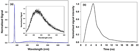
Figure 13. (a) Fluorescence spectrum excited at 387 nm. (b) Time resolved fluorescence of PEEK yielding an excited state lifetime τ ∼ 2 ns.
Download figure:
Standard image High-resolution image3.7. Micro-machining
3.7.1. Beam processing, λ = 775 nm.
Below ablation threshold, optical breakdown was observed within the PEEK polymer film resulting in material darkening, suggesting thermal decomposition due to carbonisation, figure 14(a). Scan lines result in a weak absorption grating and this effect has been reported previously [39]. In figure 14(b), overscanning results in significant material darkening while figure 14(c) shows single spot surface ablation on PEEK just above threshold at 775 nm. Here, line scans produce white light surface diffraction.

Figure 14. (a) Observed material carbonisation due to optical breakdown inside 50 µm thick amorphous PEEK just below ablation threshold (775 nm, F = 1.36 J cm−2, s = 1 mm s−1, hatch 10 µm) creating a weak internal grating, (b) carbonisation (left) and white light (WL) diffraction (right) from line scans of surface ablation just above ablation threshold at 775 nm, (c) optical image of surface ablation spots (775 nm, F = 2.9 J cm−2, s = 5 mm s−1).
Download figure:
Standard image High-resolution imageFigures 15(a) and (b) show the University of Liverpool logo machined using 775 nm at fluence F = 2.74 J cm−2 and scan speed s = 5 mm s−1 demonstrating that high contrast marking can be achieved. Carbonisation occurs with multi-pulse exposure due to both optical breakdown and polymer thermal decomposition.
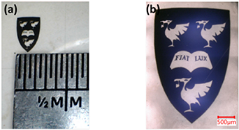
Figure 15. (a) Marking of University of Liverpool logo at 775 nm. (b) Optical image of the logo machined at 775 nm, F = 2.74 J cm−2 and scan speed s = 5 mm s−1 demonstrating a high contrast mark is obtained due to the carbonisation during ablation.
Download figure:
Standard image High-resolution image3.7.2. Beam processing, λ = 387 nm.
Figures 16(a)–(d) show optical, SEM and Wyko images of a micro-machined 8 × 8 chess board with 50 µm squares (9 µm deep) and excellent edge quality. The absence of re-deposited material around the exposed areas is consistent with more evaporative ablation, although surface roughening occurs, creating light scatter, evident in figure 16(a).

Figure 16. (a) Microscope optical image of a chess board machined at 387 nm on 50 µm PEEK. Lens focal length was 100 mm and focus spot size ∼ 34 μm, F = 0.8 J cm−2, s = 1 mm s−1, 3 overscnas. The dark regions are due to optical scattering from increased roughness, (b) SEM image of the squares showing excellent edge quality, (c) 3D Wyko image of the chess board, (d) cross section of the 9 μm deep squares.
Download figure:
Standard image High-resolution image3.7.3. Laser induced periodic surface structuring at λ = 387 nm.
At normal incidence, with fluence near damage threshold, the excitation of surface scattered waves and their interference with the incoming wave leads to an inhomogeneous energy deposition, generating periodic surface structures with pitch given by Λ ∼ λ or λ/n where n is the material refractive index [40], and termed low spatial frequency LIPSS (LSFL). Direction is typically at right angles to the laser polarisation on metals with fluence near ablation threshold. In polymers, however, with UV ns pulse lengths, these ripples can be created using fluence well below ablation threshold combined with very high pulse numbers (many thousands) and generally align parallel to the incident electric field [41]. At amorphous polymers surface, the temperature should exceed the glass transition temperature Tg allowing polymer segmentation and chain dynamics [22]. With ultrashort pulse lengths, periodic structures can also appear with low fluence/high pulse numbers [20] as well as fluence near ablation threshold [41]. LIPSS formation may also involve self-organisation [22] and the finesse of the LIPSS also depends on exposure so that a feedback mechanism is invoked.
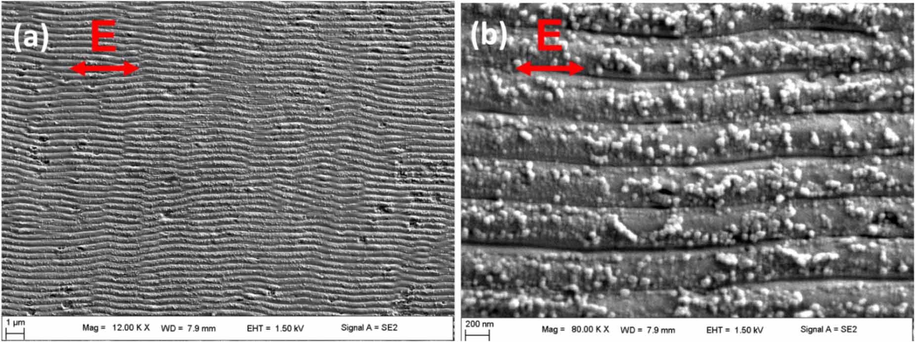
The quality of NUV ablation and the observation of LIPSS structures during blind hole machining (figure 4) indicated that it should be relatively easy to generate large area LIPSS during laser scanning with incident linear polarisation Figures 17(a)–(d) confirm that this is indeed the case on 200 µm thick PEEK. White light diffraction from 1 cm2 micro-structured areas are shown in figures 17(a) and (b) at slightly different angles while figures 17(c) and (d) show a chessboard pattern (2 mm squares) with LIPSS rotated by 90° on alternate squares. Figure 18 shows SEM images of the LIPSS confirming that the pitch Λ ∼ 0.38 μm ∼ λ with the direction of LIPSS parallel to the direction of linear polarisation | V > during scanning. Figure 18(b) also shows that there are very fine nano-particles (ϕ < 50 nm) re-deposited on the surface.
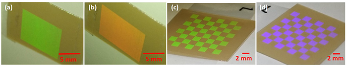
Figure 17. LIPSS on 200 µm thick PEEK (F = 0.52 J cm−2, 1 overscan, f = 100 mm). (a), (b) Large area diffraction from 1 cm square areas at different angles, (c) high angle white light diffraction from chessboard pattern, 2 mm squares with polarisation rotated alternately by 90°, (d) WL from chessboard sample rotated 90° confirming that LIPSS rotate with linear polarisation direction.
Download figure:
Standard image High-resolution image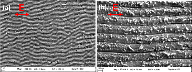
Figure 18. (a) SEM image of surface LIPSS, (b) high magnification SEM image of LIPSS showing that the pitch is close to the wavelength. Note also that fine re-deposited nano-particles (ϕ < 50 nm) appear on the surface. The beam was defocused (f = 100 mm) away from the surface to a beam diameter ϕ ∼ 100 μm and scan speed = 3 mm s−1 hence pulse overlap N ∼ 97% with fluence F = 0.52 J cm−2.
Download figure:
Standard image High-resolution image3.7.4. Raman spectroscopy.
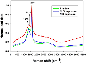
After surface LIPSS patterning, the resulting periodic structures were coated with approximately 10 nm of gold to enhance the Raman signal. Raman spectra (λex = 325 nm) of the pristine and patterned areas were compared to identify any changes in the polymer molecular structure during fs laser exposure. Figure 19 shows two main peaks at 1607 cm−1 and 1368 cm−1 which correspond to vibrations of the C = C bond and symmetric stretch of the C-H bond respectively [42] while the shoulder near 1414 cm−1 may be due to C–O and C–O–C vibrations. For comparison, a Raman spectrum of the NIR exposed surface is shown. While the same peaks appear in both NIR and NUV structured areas, the level of background fluorescence with NUV exposure is only marginally higher than pristine material, while NIR processing has a higher level of scatterring, the source of which is not yet entirely clear.
Figure 19. Raman spectra of the amorphous PEEK (pristine, NIR and NUV exposure). The two main peaks correspond to C = O and C–H vibrations. No new peaks appear in the Raman spectra but the background fluorescence is highest with NIR exposure. The spectra are all normalised using the most intense peak at 1607 cm−1.
Download figure:
Standard image High-resolution image
4. Discussion and conclusions
Laser ablation of amorphous PEEK has been demonstrated with ultrahigh intensity fs laser pulses at 775 nm and 387 nm. With single pulse ablation threshold measured to be 2.01 J cm−2 and 0.23 J cm−2 respectively. Multi-pulse, 180 fs NIR ablation also leads to material darkening and carbonisation through optical breakdown and polymer thermal de-composition hence useful primarily for high contrast marking.
The significant difference in ablation threshold is likely due to the change in NL order from 3-photon (4.8 eV) at 775 nm (proceeding through virtual states) to 2-photon at 387 nm which has a photon energy just within the material bandgap, increasing the probability of further sequential photon absorption from the excited states at 3.2 eV in the conduction band to levels where the density of states in PEEK (at 6.4 eV) is even higher [4]. This could allow reverse saturation absorption (RSA) with an absorption cross section well exceeding the ground state absorption cross section σ387 [31] and estimated here to be 1 order of magnitude higher than that from the ground state to the conduction band. This leads to a very high level of excitation in the conduction band, consistent with the low ablation threshold. The measurement of an intensity dependent effective 2-photon absorption coefficient β = β(I0) using the open aperture Z scan technique supports RSA as the primary absorption meachanism at 387 nm, however, the estimated 2-photon absorption coefficient from Z scan multi-pulse data yields < β(I)I > ∼ 6.103 cm−1 certainly much greater than the linear absorption coefficient, α(387) = 300 cm−1 but not as high as is indicated by the the multi pulse (N > 20) optical penetration depth (∼100 nm) which requires an effective absorption coefficient of ∼ 105 cm−1. This suggests that incubation leads to a rapid increase in absorption coefficient at 387 nm after a few pulses.
Transitions to the conduction band near 3.2 eV occur from the highest occupied levels in the valence band corresponding to degenerate e1 g electronic levels of benzene [36] and Raman spectroscopy shows a strong peak at 1607 cm−1 corresponding to the C = C bond excitation.
Two-photon absorption at 387 nm couples 6.4 eV energy to the material and this absorbed energy is adequate to break all the polymer bonds except the C = O (8.28 eV) which has higher energy. Further sequential photon absorption is also possible (3 PA), coupling 9.6 eV, well above the calculated ionisation potential of PEEK (7.0 eV). Thus, direct polymer photo-decomposition of amorphous PEEK is likely with NUV ultrahigh intensity pulses and supported by the observed high quality polymer ablation.
Consequently, it is straight forward to create plasmonic sub-micron surface LIPSS with a pitch near the NUV wavelength, corresponding to a line density > 2000 l mm−1. Surface scanning near ablation threshold produced areas diffractive to white light, with directional rotation with linear polarisation. These nano-structures may well be useful for applications in improving tribological performance, such as wear resistant surfaces or control of biological cell orientation [22]. While PEEK is a suitable bio-material, for example, in orthopaedic applications, it has a poor interfacial bio-compatability due to its chemical stability—hence surface modification by the addition of LIPSS might well improve its bio-compatability [2].
Finally, the advantage of using femtosecond polymer ablation with a photon energy within the material bandgap reduces ablation thresholds significantly over NIR multi-photon ablation which can only proceed via virtual transitions requiring much higher intensities.
Acknowledgments
We acknowledge valuable discussions on RSA with Professor Robert W Boyd and his post-doctoral fellow, Dr Akbar Safari, Department of Physics, University of Ottawa, Canada. Finally, we acknowledge Dr Paul Everitt of Goodfellow Cambridge Ltd. who provided the 75 μm thick PEEK film.