


Introduction
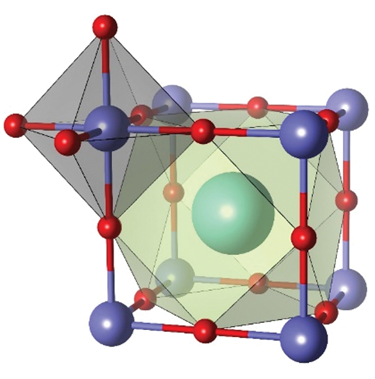
The name “perovskite” honors Russian mineralogist L.A. Perovski, who first characterized the structure of the mineral calcium titanium oxide (CaTiO3). A perovskite material has the chemical formula of ABX3, where A is a cation with a large ionic radius, B is a metal cation, and X is an anion; its crystallographic structure is the same as that of CaTiO3. The easiest way to describe the perovskite structure is to display it as an AX12 cuboctahedron that shares its edges with a BX6 octahedron, as shown in Figure 1.Reference Xu, Cho, Kim, Kim, Wolf, Park and Lee1 This oxide perovskite structure is energetically stable and is flexible enough to structurally accommodate a variety of elements, which facilitates adjustment and choice of materials to achieve the desired properties. Through successful application as dielectric and piezoelectric materials, the excellent structural properties that are achieved can be used in almost any application, such as superconductors, multiferroics, batteries, fuel cells, photovoltaic electrodes, catalysts, resistive switches, and sensing materials.Reference Kubicek, Bork and Rupp2–Reference Yin, Weng, Ge, Sun, Li and Yan4

Figure 1. Wide range of applications based on halide perovskite materials and crystallographic structure. Reprinted with permission from Reference 1. © 2016 Wiley.
Halide perovskites have the same perovskite structure as oxide perovskites, but monovalent halide ions occupy the sites populated by divalent oxygen ions in an oxide perovskite. Therefore, halide perovskites can only host inorganic metal cations, such as Pb2+, Sn2+, and Ge2+, with a valence state of 2+ to satisfy charge neutrality. This means that diversity in terms of composition can be greatly limited compared to that of oxide perovskites which can also accept trivalent and tetravalent cations at the B site. This limitation, however, is compensated by the possibility of lower-temperature synthesis of halide perovskites compared to oxide perovskites. This allows organic cations to be accommodated in the halide perovskite and has led to the development of a new class of materials called inorganic–organic hybrid halide perovskites.
Inorganic–organic hybrid perovskites are well known for their success in solar power generation. In 1978, WeberReference Weber5 had already studied the basic crystallographic properties. The acceptance of organic cations in the A position of the perovskite structure could yield new properties that conventional oxide perovskites do not have, which presents a new avenue in materials science. Moreover, organic cations allow easy conversion of a three-dimensional (3D) perovskite to a two-dimensional (2D) structure depending on the size of the ions, and new categories of material groups are expected to be created because a combination of 3D and 2D structures is possible. For example, higher dielectric and piezoelectric properties than those of oxide perovskites BaTiO3 or Pb(Zr,Ti)O3 were observed in the 2D perovskite ferroelectric (4-aminotetrahydropyran)2PbBr4.Reference Chen, Song, Zhang, Li, Ge, Tang, Gao, Zhang, Fu, You and Xiong6 As shown in Figure 1, applications using halide perovskites continue to expand to optoelectronic devices, such as solar cells and light-emitting diodes (LEDs); nanoelectronic devices such as thermoelectric and memory devices; and artificial synapses.Reference Liu, Zhao, Li, Liu, Liscio, Milita, Schroeder and Fenwick7–Reference Hong, Le, Kim and Jang9
Inorganic–organic hybrid perovskite materials such as methylammonium lead triiodide, formamidinium lead triiodide, and formamidinium tin triiodide are especially attracting increasing attention owing to their unique and interesting optical and electrical properties, such as high molar extinction coefficient, tunable bandgap, and low excitation binding energy, and are thus becoming popular targets for exploring new properties. A high power-conversion efficiency, defined as the ratio of energy output from the solar cell to input energy from the sun, of up to 25.2% has been certified for perovskite photovoltaic solar cells,10 but this is still much lower than the theoretical Shockley–Queisser (S–Q) efficiency (>30%), which is the maximum efficiency for any type of single junction solar cell. To further increase the efficiency of the halide perovskite solar cells, it is necessary to not only reduce trap-assisted nonradioactive (also known as Shockley–Read–Hall) recombination, but also to minimize the concentration of defects at each interface composed of a multilayer thin film, and increase light absorption via optical management. Halide perovskite-based LEDs have also achieved an amazing breakthrough in a short time. The articles in this issue provide an overview of each topic that is important to halogen perovskites and devices for optoelectronic applications.
Properties and applications of halide perovskites
One of the common characteristics of halide perovskites is the presence of ns Reference Kubicek, Bork and Rupp2 ions, which is an important factor in understanding the electronic, dielectric, and defect properties of halide materials. In a lead halide perovskite structure containing 6s Reference Kubicek, Bork and Rupp2 cations, the s state of the cation decreases in energy and moves away from the p state of the cation, establishing a lone-pair state. Significant hybridization between the occupied cation s and halogen p states (for example, overlap between Pb-6s and I-6p) endows exceptional performance to lead-based halide perovskites. The Fabini et al. articleReference Fabini, Seshadri and Kanatzidis11 in this issue introduces the 6s Reference Kubicek, Bork and Rupp2 (5s Reference Kubicek, Bork and Rupp2) lone pair electrons on Pb (Sn) and the stereochemistry thereof. The lone pairs are shown to have a decisive impact on the electronic properties, directly yielding a favorable broad valence band and light-hole states. They establish a connection between the electronic composition of the metal cation and the resulting electron-band structure and lattice dynamics of the compound.
Perovskite solar cells, which have experienced unprecedented recent efficiency gains, will significantly reduce the rate of increase in efficiency in the near future. Beyond the S–Q efficiency limit for single-junction solar cells, maximum output power can be achieved if photon recycling effects occur in the device. Specifically, there may be an optical management approach to improve the efficiency of perovskite solar cells, including the integration of plasmonic or dielectric nanostructures into the optical cavity design inside the device and its other layers. During the radiative recombination process, photons are generated by recombination of one electron–hole pair, but photons can be reabsorbed at different spatial locations in the solar cell, creating new electron–hole pairs. Designs of light capture and angular restriction can maximize solar cell efficiency by improving the photon reabsorption process. In their article in the issue, Lee et al.Reference Lee, Choi, Min, Woo and Noh12 review three major technologies for implementing photon recycling for the next phase of approaching the S–Q limit level of halide perovskite solar cells.
Halide perovskites have soft, polarizable, and dynamically disordered lattices because the ionic bond between the monovalent halide anion and divalent cation is not strong; thus, point defects form easily. These defects can critically affect the properties and operational stability of metal-halide-perovskite optoelectronic devices. For example, nonradioactive recombination caused by defects in the perovskite solar cells can be a major loss mechanism. The defects also cause significant luminescence quenching in perovskite-based LEDs. Therefore, to achieve high efficiency in both solar cells and LEDs with halide perovskites, it is necessary to create a defect-free, high-quality crystalline phase or, alternatively, to develop a deep understanding of the behavior of the defects. In their article in the issue, Kumar et al.Reference Kumar, Hodes and Cahen13 introduce the fundamentals, the unusual behavior, and the properties of defects in halide perovskites. They ask, “Can we find and identify ways to prove the presence or absence of defect tolerance?”
Xiao et al.Reference Xiao, Li, Zheng and Yang14 in their article in this issue discuss the post-treatment methods of achieving higher performance in perovskite photovoltaics. It is noteworthy that the development of new fabrication techniques and composition engineering has greatly contributed to improving the device efficiency and performance. This article overviews post-treatment methods and their impact, and summarizes the fundamentals of nonradiative energy loss in perovskite solar cells at the current level of understanding. It also reviews recent advances in mitigating the energy loss by post-treatment techniques and provides key ideas for further development.
Apart from the realization of improved efficiencies, these perovskite materials still face stability issues hindering their progress toward commercialization. In their article in this issue, Zhang et al.Reference Zhang, Rong, Hu, Mei and Han15 provide a comprehensive overview and seek solutions through hole-conductor-free perovskite solar cells. Although organic hole-transport materials, such as Spiro-OMeTAD, employed in the fabrication of solar cells yield higher efficiency, they impose a drawback of poor stability. This can be potentially addressed by excluding the hole-transport layers, which transport or extract the hole carriers generated in perovskite active layer under solar irradiation, to take advantage of the superior hole- and electron-transport properties of the perovskite itself. This strategy is presented in detail to enlighten readers, and their prospective application is discussed to pique interest among researchers. The device structure, electron-transport materials, morphology and composition of halide perovskites, electrode materials, and energy-level alignment affect the efficiency of hole-conductor-free perovskite solar cells. The strategies currently applied to optimize the efficiency of various hole-conductor-free perovskite solar cells are presented and their impact on stability and efficiency are discussed. Various device structures of hole-conductor-free perovskite solar cells are presented, and their significant stability and improved efficiency are summarized. Finally, a hint of the future scope and development trend of hole-conductor-free perovskite solar cells is provided to address their low-efficiency issue.
The advantage of tunable and narrow emissions covering the whole visible region in nanocrystalline metal-halide perovskites has invoked much interest among researchers. Perovskite nanocrystals have emerged as a new generation of light-emitting materials and have found interesting applications in optically pumped white-emissive LEDs and monochromatic electrically driven LEDs. Although the use of perovskite nanocrystals as active materials for various optoelectronic devices has been explored extensively, they face limitations for light-emitting applications arising from their low photoluminescence quantum efficiencies (PLQEs). This is because of the presence of mobile ionic defects and the small exciton-binding energy. A promising approach to improve the PLQEs is to develop techniques to prepare nanocrystals with increased exciton binding energy and reduced defects. A wide range of reports have been available since 2004 concerning this objective. Because a variety of synthetic approaches have been established to precisely control the compositions and microstructures of perovskite nanocrystals, it is important to consider such milestones in the field of materials development and device integration based on perovskite nanocrystals. In their article in this issue, Xu etal.Reference Xu, Worku, He and Ma16 summarize these recent advances in light-emitting nanocrystalline perovskites, from synthesis control to device integration. Despite tremendous development, many issues and challenges, including stability, lead poisoning, and accessible processing, remain. These are discussed to enlighten readers about the existing challenges and generate innovative ideas among young researchers to overcome them in the near future.
Outlook
Over the past decade, the performance of optoelectronic devices, such as solar cells and LEDs, based on halide perovskites, has evolved significantly in terms of efficiency and stability. In particular, halide perovskites can now be fabricated as high-efficiency devices using a low-temperature solution process. If long-term stability can be improved, the halide perovskite will become an appealing material that satisfies even low-cost requirements. Moreover, because halide perovskites can accept and incorporate organic cations within one crystal structure, new physical properties may appear depending on the type of organic cations used. Therefore, these materials are expected to be highly scalable for a variety of applications. This will require extensive research, from the basic properties to practical devices. We have briefly reviewed and highlighted various aspects of halide perovskite materials here. We hope the articles in this issue will inspire researchers to utilize these materials in a broad range of research fields, and encourage new and especially early career researchers to enter the field and contribute.
 Sang Il Seok is a distinguished professor in the School of Energy and Chemical Engineering at the Ulsan National Institute of Science and Technology (UNIST), South Korea. He obtained his PhD degree from Seoul National University, South Korea. His current research focuses on the preparation of functional inorganic–organic hybrid materials and their application to energy devices, including perovskite solar cells. In 2017, he received the Korea Scientists Award from the Korean Government, and in 2019, he received the Kyung-Ahm Prize from the Kyung-Ahm Education and Cultural Foundation. Seok can be reached by email at seoksi@unist.ac.kr.
 Tzung-Fang Guo has been a faculty member in the Department of Photonics at National Cheng Kung University, Taiwan, since 2003. He received his PhD degree in materials science and engineering from the University of California, Los Angeles, in 2002. His current research focuses on the magnetic field effect of organic electronic devices and perovskite-based photovoltaics and light-emitting diodes. He received an Academic Outstanding Research Award from the Ministry of Science and Technology, Taiwan in 2018, and became a Fellow of SPIE, the International Society for Optics and Photonics in 2020. Guo can be reached by email at guotf@mail.ncku.edu.tw.

