


Introduction
Throughout human history, major advances in technology have been usually accompanied by a revolution in materials. Examples include the invention of bronze tools after the stone age, the displacement of bronze by iron, the development of the metallurgy of steel and aluminum that has been stimulated by and has fueled the industrial revolution, and the optimization and surface passivation of silicon that enabled much of the multibillion-dollar technological sector in the present day. Today, similarly disruptive advances in quantum materials may germinate from the burgeoning field of quantum information science (QIS), which utilizes quantum degrees of freedom for information storage and processing.1 Technologies to manipulate and harness quantum states are poised to revolutionize current paradigms of computation, sensing, storage, and communications.
The term “quantum materials” is fairly broad, encompassing all materials whose properties are largely determined by quantum mechanical principles and phenomena. A key distinction of quantum materials from other materials lies in the manifestation of quantum mechanical effects at macroscopic length scales. In fact, all materials are composed of basic quantum particles and quasiparticles (i.e., electrons, holes, spins, and phonons) on the foundation of quantum mechanical principles at microscopic length scales; for example, the wave-particle duality of basic quantum particles or quasiparticles, and uncertainty in energy/momentum of basic particles or quasiparticles. However, the quantum mechanical effects manifested at the molecular and atomic scale of classical materials are overwhelmed by the classical statistical mechanics of a large particle ensemble in macroscopic length scales. Generally, quantum materials are characterized by at least one, and often several, of the following attributes.
The first attribute is the quantum confinement of basic quantum particles and quasiparticles (i.e., electrons, holes, excitons, spins, and phonons) due to the reduced dimensionality of materials. Quantum confinement occurs when the physical dimension of the materials is comparable to or smaller than the characteristic length scale of quantum particles. The definition of characteristic length scale varies with quantum particles, for instance, as the physical extension of excitonic wave function (excitonic Bohr radius) for excitons and as mean scattering-free paths for electrons, holes, spins, and phonons. Quantum confinement leads to properties that are either dramatically modified from the bulk or entirely new properties not found in the parent materials, such as the size-dependent energy-level spacing of charges in semiconductor nanocrystals that form the basis of quantum dot displays,Reference Bera, Qian, Tseng and Holloway2 and the controlled entangled spin states in semiconductor quantum dots that are now a promising platform for quantum computation.Reference Loss and DiVincenzo3
Another common attribute of quantum materials is strong many-body interactions, such as electron–electron, electron–phonon, exciton–exciton, and spin–valley interactions. For instance, the strong Coulomb interactions among charges, which, together with competing degrees of freedom such as spin and valley (local minima in the electronic band structure), gives rise to collective phenomena that are not expected from the noninteracting single-particle picture. These emergent phenomena include some of the most spectacular manifestations of collective behaviors of charges and atoms, including superconductivity, magnetism, and charge-density waves. They also underlie some of the most studied but long-standing mysteries in materials research, such as high-temperature superconductivity and heavy fermion systems.
A third characteristic shared by many quantum materials is the important role played by topology and the Berry phase (the Berry phase is a geometric phase of the wave function acquired by a charge when it adiabatically completes a closed path in certain parameter spaces). These topological quantum materials have topologically nontrivial electronic structures, giving rise to exotic properties that are topologically protected. Examples include the quantum spin Hall effect (QSH) in two-dimensional (2D) topological insulators (TIs), in which helical edge states (a pair of counter-propagating spin-polarized edge states) circulate along the edges of otherwise insulating bulk; and the quantum anomalous Hall effect (QAHE) in insulators that, in the presence of magnetization and large spin–orbit coupling, host quantized Hall conductance in a zero magnetic field.
Last, quantum materials enable the utilization of noncharge degrees of freedom of charge carriers, such as spin, valley, and pseudospin. Creation, transport, and manipulation of these nontraditional state variables has been a flourishing area of research, with technological applications beyond Moore’s Law scaling of integrated circuits, high-density storage (exemplified by the spectacular success of magnetic random-access memory [MRAM]), low-energy electronics, and quantum computation.
Here, we briefly discuss some of the most promising quantum material systems that have recently emerged as topical research areas. In most of these systems, more than one of these previously discussed attributes, are present, intertwining to give rise to novel phenomena and enabling devices to usher in new scientific and technological paradigms of computation, sensing, and communications (Figure 1).

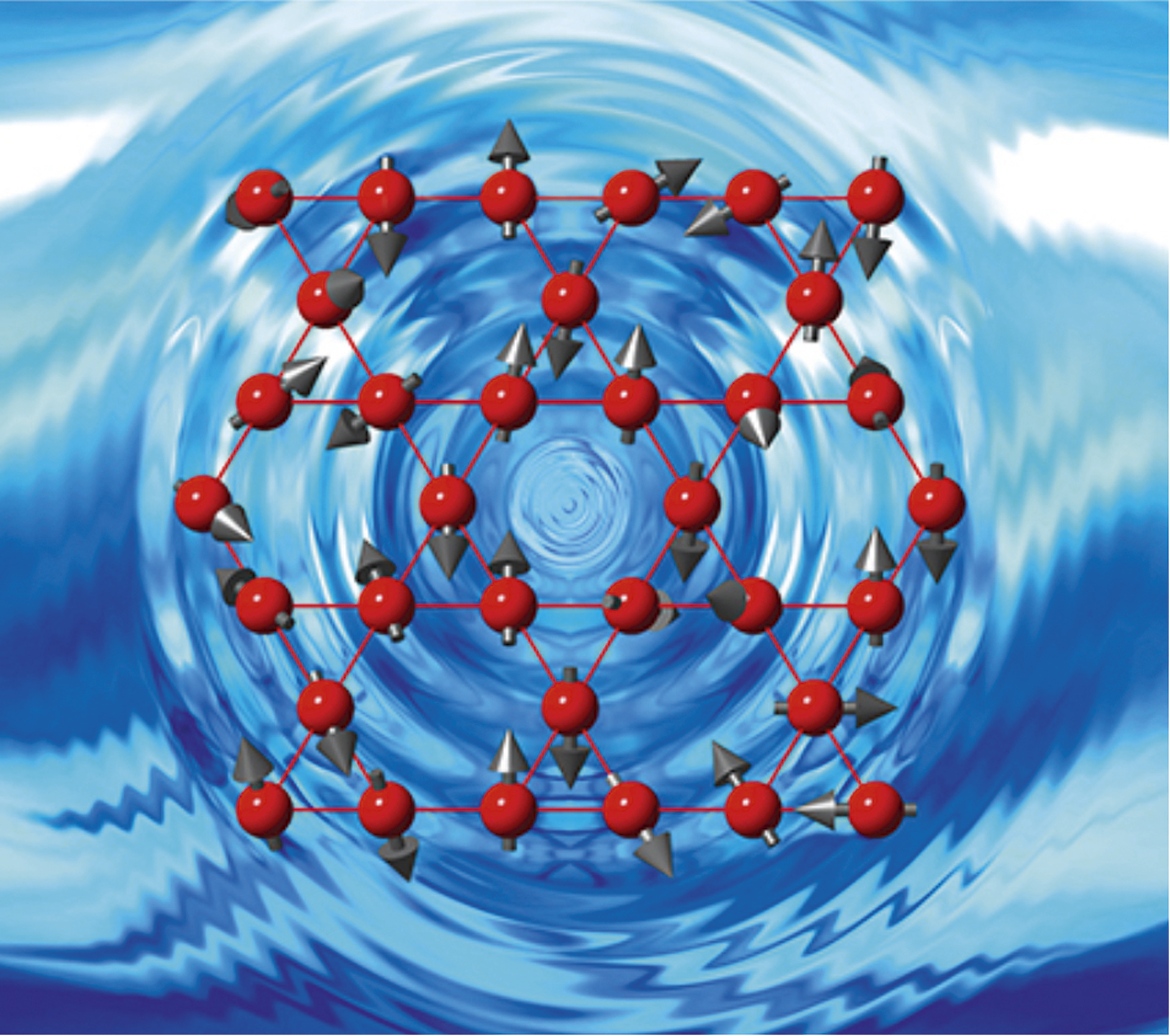
Figure 1. Quantum materials are characterized by, among other attributes, reduced dimensionality and unexpected collective phenomena such as superconductivity and magnetism that emerge at the interface of heterostructures. From left to right, the schematics show Cooper pairs, ferromagnetic ordering of charges, and light–matter interaction.
Two-dimensional materials
Two-dimensional materialsReference Butler, Hollen, Cao, Cui, Gupta, Gutierrez, Heinz, Hong, Huang, Ismach, Johnston-Halperin, Kuno, Plashnitsa, Robinson, Ruoff, Salahuddin, Shan, Shi, Spencer, Terrones, Windl and Goldberger4 have constituted one of the most active frontiers of materials research in the past decade, opening the door for exploring the mechanical, optical, thermal, and electronic properties of atoms that are confined to atomically thin layers and with promise as the future generation of electronic and optoelectronic materials and applications. Starting with the isolation of graphene on insulating substrates,Reference Novoselov, Geim, Morozov, Jiang, Zhang, Dubonos, Grigorieva and Firsov5 the family of 2D materials has since been broadened to include insulators, semiconductors, superconductors, ferromagnets, and charge-density wave materials.
The allure of 2D materials partly lies in their extremely reduced dimensionality—as a material’s thickness is reduced to a single or few atomic layers (Figure 2a), its properties are dramatically altered from those of the bulk. As a result of the reduced dimensionality, 2D materials often feature strong quantum confinement and reduced Coulomb screening. The quantum confinement gives rise to discrete energy levels, and the reduced Coulomb screening can significantly enhance the effects of charge interactions. From an intuitive perspective, the enhanced charge interaction results from the fact that the charges simply do not have as much available “space” to avoid one another (in fact, they “have lost” an entire dimension). The strong quantum confinement and reduced Coulomb screening collectively enable the exceedingly strong exciton binding energy in 2D materials, in particular, 2D semiconductors, which is often more than one order of magnitude stronger than that of conventional semiconductors. Such strong binding energy makes excitons, a quasiparticle consisting of electrostatically bound electrons and holes, robust enough to become a viable carrier for quantum information processing. This will be discussed further in the section on strongly correlated quantum materials.

Figure 2. Tunability of 2D materials. (a) Schematic of crystal structure of bilayer MoS2. Yellow and green atoms represent S and Mo, respectively. (b) Phase diagram for monolayer WTe2, which can be a quantum spin Hall (QSH) insulator, superconductor (SC), or metal depending on charge density.Reference Mayorov, Elias, Mukhin, Morozov, Ponomarenko, Novoselov, Geim and Gorbachev6,Reference Kim, Baik, Ryu, Sohn, Park, Park, Denlinger, Yi, Choi and Kim19 (c) (Left) Few-layer phosphorene is predicted to (right) transition among metal, topological insulator, and normal insulator states as a function of electric field.Reference Drögeler, Franzen, Volmer, Pohlmann, Banszerus, Wolter, Watanabe, Taniguchi, Stampfer and Beschoten8 The box indicates the unit cell of few-layer phosphorene. (d) Phase diagram of ABC-stacked trilayer graphene at the charge neutrality point in the quantum Hall regime, transitioning among layer antiferromagnet (LAF), canted antiferromagnet (CAF), ferromagnet (F), and quantum valley Hall insulator (QVH).Reference Lee, Tran, Myhro, Velasco, Gillgren, Lau, Barlas, Poumirol, Smirnov and Guinea21 The arrows indicate spin configurations on different layers of the trilayer. Note: n, charge density; T, temperature; U ⊥, out-of-plane potential difference; B ||, perpendicular electric field.
Combining these effects with additional degrees of freedom, such as spin, valley, and layer, results in many specular phenomena in quantum materials, including emergent quantum phases such as magnetism, superconductivity, or correlated insulators that are not found in their bulk counterparts. In many cases, two or more of these quantum phases manifest in the same material and are tunable in situ by charge injection via electrical gating or other ways. Two-dimensional quantum materials are also extremely attractive from the standpoint of providing unprecedented quality and tunability. First, many 2D materials have an exceedingly high charge mobility, which exceeds several million cm2/Vs in graphene,Reference Mayorov, Elias, Mukhin, Morozov, Ponomarenko, Novoselov, Geim and Gorbachev6 and reaches up to 25,000 cm2/Vs in few-layer black phosphorus.Reference Yang, Tran, Wu, Che, Taniguchi, Watanabe, Baek, Smirnov, Chen and Lau7 Such high mobilities are particularly pertinent for applications that require long lifetimes for charge or spin. For instance, spin lifetimes as long as 12 ns have been demonstrated.Reference Drögeler, Franzen, Volmer, Pohlmann, Banszerus, Wolter, Watanabe, Taniguchi, Stampfer and Beschoten8,Reference Xu, Zhu, Luo, Lu and Kawakami9 Second, 2D materials are extremely tunable, as many of the properties can be controlled via electrostatic gates that can tune charge density and the out-of-plane electric field, as well as via in-plane and out-of-plane magnetic fields. For instance, while bulk WTe2 is a semimetal, monolayer WTe2 is a QSH insulator at low doping and becomes a superconductor when the charge density exceeds 5 ×1012 cm–2 (Figure 2b).Reference Qian, Liu, Fu and Li10–Reference Sajadi, Palomaki, Fei, Zhao, Bement, Olsen, Luescher, Xu, Folk and Cobden16 In highly doped atomically thin MoS2, Ising superconductivity is observed, in which the spin-valley locking leads to an in-plane critical field that greatly exceeds the paramagnetic limit.Reference Lu, Zheliuk, Leermakers, Yuan, Zeitler, Law and Ye17 Few-layer black phosphorus has been predicted and shown to undergo transitions among normal insulator, topological insulator, and semimetal as a function of out-of-plane electric field (Figure 2c).Reference Liu, Zhang, Abdalla, Fazzio and Zunger18,Reference Kim, Baik, Ryu, Sohn, Park, Park, Denlinger, Yi, Choi and Kim19 In bilayer and ABC-stacked trilayer graphene, transitions among layered antiferromagnet, layer polarized valley–Hall insulator, and conventional metal by changing charge density n and out-of-plane potential bias U ⊥ (Figure 2d).Reference Velasco, Jing, Bao, Lee, Kratz, Aji, Bockrath, Lau, Varma, Stillwell, Smirnov, Zhang, Jung and MacDonald20–Reference Maher, Dean, Young, Taniguchi, Watanabe, Shepard, Hone and Kim22 Bilayer CrI3 can be ferromagnetic, antiferromagnetic, or paramagnetic depending on doping level and magnetic field.Reference Huang, Clark, Klein, MacNeill, Navarro-Moratalla, Seyler, Wilson, McGuire, Cobden, Xiao, Yao, Jarillo-Herrero and Xu23–Reference Jiang, Shan and Mak25
Third, the electronic states in 2D materials are surface states, and thus are more easily manipulated and coupled to mechanical, optical, or scanned probes. They are nature’s thinnest elastic membranes,Reference Pereira and Castro Neto26,Reference Vandeparre, Pineirua, Brau, Roman, Bico, Gay, Bao, Lau, Reis and Damman27 and can ripple,Reference Bao, Miao, Chen, Zhang, Jang, Dames and Lau28 wrinkle,Reference Bao, Myhro, Zhao, Chen, Jang, Jing, Miao, Zhang, Dames and Lau29,Reference Zhang, Huang, Velasco, Myhro, Maldonado, Tran, Zhao, Wang, Lee, Liu, Bao and Lau30 and sustain elastic strains up to 25%.Reference Lee, Wei, Kysar and Hone31 They are excellent optoelectronic materials and provide ultrafast and broadband photoresponse.Reference Xia, Mueller, Lin, Valdes-Garcia and Avouris32–Reference Liu, Chang, Norris and Zhong38 Finally, they enable creation of twist, Moiré, or stacked heterostructures with tailored electronic properties that are otherwise inaccessible (see also the next section on ‘Heterostructures and interfaces’).
Heterostructures and interfaces
In a heterostructure, two dissimilar materials are adjoined together to form a new material system. At the interface of the two dissimilar materials, the mismatch in work functions, Fermi velocities, electronic bands, magnetic ordering, and lattice constants results in a plethora of new phenomena. One of the oldest and most intensely studied phenomena is the discontinuity in conduction and valence bands of semiconductors with different doping or bandgap sizes, which leads to the formation of a quantum well, 2D electron gas (2DEG) or 2D hole gas at the interface of semiconductor heterostructures (Figure 3a). Remarkably, a 2DEG may even emerge at the interface of insulators, such as in the case of LaAlO3/SrTiO3,Reference Ohtomo and Hwang39–Reference Burg, Prasad, Kim, Taniguchi, Watanabe, MacDonald, Register and Tutuc43 where both of the parent materials are insulators (with bandgaps of 5 eV and 3.5V, respectively). Under the right conditions, a number of surprising phenomena have been observed at this interface, including high mobility transport, quantum oscillations, superconductivity, ferromagnetism, and giant photoconductivity.
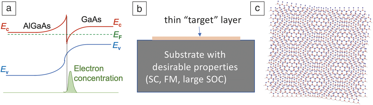
Figure 3. (a) Band structure of GaAs/AlGaAs heterostructures. The mismatch of bands at the interface gives rise to the inversion that hosts a 2D electron gas. (b) Schematic of the modification of material property by proximization with a substrate that has the desirable attribute, such as superconductivity (SC), ferromagnetism (FM), and large spin–orbit coupling (SOC). (c) Moiré superlattice in twisted bilayer graphene. Note: E C, conduction-band minimum; E V, valence-band minimum; E F, Fermi energy.
Apart from the misalignment of band structures, other important factors at the interface are interfacial charge transfer (e.g., mismatch in work functions) and lattice mismatch. For instance, bulk FeSe is a superconductor with intrinsic transition temperature T c ∼ 9 K; amazingly, for a FeSe monolayer on SrTiO3 substrate, its T c skyrocketed by as much as an order of magnitude, to ∼100 K.Reference He, He, Zhang, Zhao, Liu, Liu, Mou, Ou, Wang, Li, Wang, Peng, Liu, Chen, Yu, Liu, Dong, Zhang, Chen, Xu, Chen, Ma, Xue and Zhou44,Reference Huang and Hoffman45 The exact mechanism of such a dramatic enhancement in T c is still under debate, but it is clearly an interfacial effect, likely related to charge transfer from SrTiO3 and interfacial phonon coupling; understanding this system could provide guiding principles for rational design of high-Tc superconductors.
Additionally, the 1.8% lattice mismatch between graphene and hexagonal BN (hBN) leads to a Moiré superlattice with a unit cell that is as large as 200 nm;Reference Bera, Qian, Tseng and Holloway2 therein the disproportion between flux quantum and the large unit cell of the Moiré superlatticeReference Ponomarenko, Gorbachev, Yu, Elias, Jalil, Patel, Mishchenko, Mayorov, Woods, Wallbank, Mucha-Kruczynski, Piot, Potemski, Grigorieva, Novoselov, Guinea, Fal’ko and Geim46–Reference Wang, Cheng, Martynov, Miao, Jing, Taniguchi, Watanabe, Aji, Lau and Bockrath49 leads to the celebrated Hofstadter butterfly fractal spectrum.Reference Hofstadter50
An important effect in heterostructures is the proximity effect, that is, the “endowment” of new properties onto a thin overlayer material by the proximity of a second material (Figure 3b). For example, spin–orbit coupling (SOC) is small in pristine graphene, but can be made much larger by proximitized graphene with transition-metal dichalcogenide layers,Reference Avsar, Tan, Taychatanapat, Balakrishnan, Koon, Yeo, Lahiri, Carvalho, Rodin, O’Farrell, Eda, Castro Neto and Özyilmaz51–Reference Wang, Che, Cao, Lyu, Watanabe, Taniguchi, Lau and Bockrath63 thus allowing the creation of devices with controlled, spatially varying SOC. The anomalous Hall effect, typically present only in ferromagnetic materials, is observed in graphene on ferromagnetic insulators.Reference Wang, Tang, Sachs, Barlas and Shi64 Another example is the opening of an energy gap in the otherwise gapless electronic structure of pristine graphene, by aligning it with hBN and breaking the inversion symmetry of the lattice.Reference Hunt, Sanchez-Yamagishi, Young, Yankowitz, LeRoy, Watanabe, Taniguchi, Moon, Koshino, Jarillo-Herrero and Ashoori47 In a technologically relevant case, proximitizing a topological insulator with a superconductor gives rise to the formation of Majorana zero modes at the interface. Majorana fermions in solid state systems are quasiparticle excitations with half-integer spins that are their own antiparticles; because they obey non-Abelian statistics, they are seen as one of the most promising routes to realize topological quantum computing. Such Majorana zero modes have been realized in heterostructures consisting of superconductor-coupled QSH or nanowire systems that have large SOC.Reference Hasan and Kane65–Reference Masatoshi and Yoichi67
The immense potential for heterostructure creation is further highlighted by the rise of “twistronics,”Reference Bistritzer and MacDonald68–Reference Cao, Fatemi, Demir, Fang, Tomarken, Luo, Sanchez-Yamagishi, Watanabe, Taniguchi, Kaxiras, Ashoori and Jarillo-Herrero71 which uses the relative twist angle between two atomic layers to tailor the electronic, thermal, and optoelectronic properties (Figure 3c). This is exemplified by the breakthrough in twisted bilayer graphene, which hosts electronic phases, including superconductivity, the QAHE, and correlated insulating state at different charge densities.Reference Cao, Fatemi, Fang, Watanabe, Taniguchi, Kaxiras and Jarillo-Herrero70–Reference Yankowitz, Chen, Polshyn, Watanabe, Taniguchi, Graf, Young and Dean74 Strictly speaking, twisted bilayer graphene is not a heterostructure; however, twistronics can be extended to twisted bilayers of different materials. For example, exotic quantum phases are expected in twisted heterobilayers, such as WSe2/MoSe2; many of these phases have nontrivial topological characteristics, such as QSH, QAH, and topological superconductors.Reference Wu, Lovorn, Tutuc, Martin and MacDonald75–Reference Xue and MacDonald77 Thus, by judicious choice of materials and device architecture, there are almost limitless possibilities for exploration of new phenomena and rational design of quantum devices.
Topological quantum materials
Topology is a mathematical concept that refers to the properties of an object that are unaffected by continuous deformation of shape, such as twisting, bending, or stretching. For example, an orange is topologically equivalent to a banana, but both are distinct from a bagel. In the 1970s, this mathematical concept was adopted by physicists to understand, for example, the quantum Hall (QH) effect in 2D systems and phase transitions in superfluids. In 2016, the Nobel Prize in Physics was awarded to Kosterlitz, Thouless, and Haldane for their “theoretical discoveries of topological phase transitions and topological phases of matter.”
The earliest and most studied topological phenomenon is the QH effect.Reference Prange and Girvin78 In a high magnetic field, electron orbitals confined to two dimensions coalesce to form Landau levels that are energetically separated by cyclotron gaps. When the chemical potential is located between Landau levels, the bulk is insulating; at the sample’s edge, however, dissipationless one-dimensional (1D) edge states form, giving rise to zero longitudinal resistance and Hall conductance that is quantized in integer multiples of e 2/h, where e is the electron charge and h is Planck’s constant (Figure 4a). It can be shown that the QH states can be mapped into a topologically nontrivial Hilbert space, with a topological invariant number, called the Chern number, which is determined by the integral of the Berry phase over the Brillouin zone. In QH systems, the time-reversal symmetry (TRS) is broken by an external magnetic field.

Figure 4. (a) Chiral edge states (red arrows) in a 2D electron gas in the quantum Hall (QH) regime in an external magnetic field (B). (b) Formation of surface states at the interface of two semiconductors that have normal and inverted bandgap, respectively. Red and green represent conduction and valence bands, respectively. (c) Helical edge states (red and green arrows) in a quantum spin Hall (QSH) insulator or 2D topological insulator (i.e., a pair of edge states that counterpropagate and their spin orientations are locked with their momenta). (d) Edge states in a quantum anomalous Hall (QAH) insulator, in this case a 2D topological insulator doped with magnetic dopants.
It is, however, possible to generate QH-like edge states without breaking the TRS.Reference Kane and Mele79–Reference Suzuki, Harada, Onomitsu and Muraki88 This groundbreaking idea was first proposed by Kane and Mele,Reference Kane and Mele79 and also independently by Bernevig and Zhang,Reference Bernevig, Hughes and Zhang82,Reference Bernevig and Zhang89 and experimentally realized in topological insulators found in CdTe/HgTe/CdTe quantum wells.Reference Konig, Wiedmann, Brune, Roth, Buhmann, Molenkamp, Qi and Zhang90,Reference Roth, Brüne, Buhmann, Molenkamp, Maciejko, Qi and Zhang91 Due to the large SOC in HgTe, the bulk electronic band has an inverted gap, that is, the hole-like valence band is energetically located above the electron-like conduction band. CdTe, however, has a normal gap. At the interface, the inverted bands in HgTe must connect smoothly to the normal bands of CdTe, thus leading to crossing of these bands at the surface (Figure 4b), in this case, the edge. The edge states are gapless and enable metallic transport; since their presence is protected by the topology of the system, their conduction is immune from scattering due to disorder or defects, similar to those at the edges of QH systems. These states are called quantum spin Hall insulator states in a 2D topological insulator (TI).
There are, however, important differences between the edge states in a TI and in a QH system. QH edge states are chiral (i.e., propagating clockwise or counterclockwise in the sample). In contrast, due to the preserved TRS, the QSH edge states in a TI come in pairs that are time-reversed partners (i.e., an edge state with spin up propagates clockwise and another with spin down propagates counterclockwise [Figure 4c]). These states are known as helical edge states or have spin–momentum locking. One of the most important applications of QSH states is topological quantum computation—coupling the helical edge states to s-wave superconductors creates Majorana zero modes at the interface, which are the building block of fault-tolerant quantum computers.
In another major breakthrough in the area, researchers realized that, instead of an external magnetic field, TRS can also be explicitly broken by proximitizing with a magnetic layer or doping a TI film with magnetic elementsReference Yu, Zhang, Zhang, Zhang, Dai and Fang92–Reference Chang, Zhang, Feng, Shen, Zhang, Guo, Li, Ou, Wei, Wang, Ji, Feng, Ji, Chen, Jia, Dai, Fang, Zhang, He, Wang, Lu, Ma and Xue95 (Figure 4d). For instance, in Cr-doped (Bi,Sb)2Te3 thin films, quantized Hall conductance of e Reference Bera, Qian, Tseng and Holloway2/h is observed at an external magnetic field B = 0.Reference Chang, Zhang, Feng, Shen, Zhang, Guo, Li, Ou, Wei, Wang, Ji, Feng, Ji, Chen, Jia, Dai, Fang, Zhang, He, Wang, Lu, Ma and Xue95–Reference Checkelsky, Yoshimi, Tsukazaki, Takahashi, Kozuka, Falson, Kawasaki and Tokura97 In this the so-called quantum anomalous Hall (QAH) insulator, the edge states are chiral, similar to that of a QH state (Figure 4d). A significant technical challenge is the low operating temperature (T ∼ 30 mK in initial experiments, ∼1 K in subsequent works with further material optimizationReference Mogi, Yoshimi, Tsukazaki, Yasuda, Kozuka, Takahashi, Kawasaki and Tokura98). More recently, a robust QAHE has been observed in intrinsic materials, including in the antiferromagnetic layered TI MnBi2Te4,Reference Deng, Yu, Shi, Guo, Xu, Wang, Chen and Zhang99 in twisted bilayer grapheneReference Serlin, Tschirhart, Polshyn, Zhang, Zhu, Watanabe, Taniguchi, Balents and Young73 and in aligned hBN/trilayer graphene Moiré superlattice.Reference Chen, Sharpe, Fox, Zhang, Wang, Jiang, Lyu, Li, Watanabe, Taniguchi, Shi, Senthil, Goldhaber-Gordon, Zhang and Wang100 QAH insulators are highly promising platforms for dissipationless spintronics with tunable domain walls or domain boundaries that can be manipulated by an electric field.
Today, the study of topological materials, including, but not limited to, topological insulators, topological crystalline insulators, Weyl semimetals, and topological superconductors, is a thriving and ever-expanding field, while the concept of topologically protected transport has been extended to the fields of photonics, phononics, mechanics, and magnonics. Topological materials are now ubiquitous, with many more novel phenomena and applications that await exploration.
Strongly interacting quantum materials
Strong many-body interactions are at the heart of the most spectacular of correlated phases that depend on the collective behaviors of charges and atoms. Here, we will briefly touch upon two systems not discussed in the previous sections: quantum spin liquid and exciton condensates.
A quantum spin liquid is an exotic phase of quantum magnetism.Reference Knolle and Moessner101–Reference Broholm, Cava, Kivelson, Nocera, Norman and Senthil103 For ferromagnets and antiferromagnets, the semiclassical picture is the establishment of long-range order of aligned or anti-aligned neighboring spins below the transition temperature (Curie or Neél temperature). In a quantum spin liquid, however, the strong interactions among spins prevents long range spin coherence even at the lowest temperature (Figure 5a).Reference Imai and Lee104 They exhibit massive quantum superposition and an unusually high degree of entanglement. This many-body quantum entanglement can support a variety of nonlocal excitations that depend on the collective behaviors of a large number of spins and charges. One of the most famous examples is so-called spinons, which are spin-1/2 quasiparticles with charge 0. Another example is the anyon, found in fractional QH states in 2DEGs, an excitation that behaves as if it carries a charge of a fraction of e; anyons obey non-Abelian statistics (i.e., they pick up a nontrivial Berry phase when circling each other). Prospective applications of this rather exotic state of matter include topological quantum computation and unconventional high-temperature superconductivity. There has been much excitement and progress in this area, though many questions, both experimental and theoretical, await answers.

Figure 5. (a) Illustration of a quantum spin liquid.Reference Imai and Lee104 Red atoms represent elementary excitations of the spin liquid, such as spinons and anyons, that carry spin and unusual charge other than electronic charge, e. (b) Schematic illustration for the condensation process of gas-like free excitons into liquid-like electron–hole liquid. (c) Schematic of indirect exciton condensate formed in bilayers of transition-metal dichalcogenides. Yellow, dark blue, and light blue atoms represent S, Mo, and W, respectively. Courtesy of J. Shan, Cornell University.
Excitons are bound pairs of electrons and holes. As a composite particle of two fermions, an exciton is a boson and obeys Bose–Einstein statistics. Excitons, therefore, have the ability to form a condensate (i.e., with macroscopic occupation of the lowest energy state). Direct excitons consist of an electron in the conduction band and a hole from the valence band from the same 2D layer. For indirect excitons, in contrast, the constituent electrons and holes originate from different layers, and their lifetime is generally much longer due to the physical separation of the electrons and holes. When the density is low, excitons behave like free gas molecules with weak interaction among neighboring excitons. A boson condensate that formed in this low-density regime is called a Bose–Einstein condensate (BEC). In the high-density regime, the excitons are similar to Cooper pairs in superconductors—the electrons and holes may be physically separated over considerable distance, and the wave function of the macroscopic ground state consists of many spatially overlapping electron–hole pairs. A condensate of these excitons is the so-called Bardeen–Cooper–Schrieffer (BCS) type, named after the BCS theory for conventional superconductors. Experimentally, exciton condensation of both BEC and BCS types has been realized in coupled quantum wells based on GaAs.Reference Butov105,Reference Eisenstein106
Both BEC and BCS exciton condensations occur in energy/momentum space. There is another type of exciton condensation in real space that is similar to the condensation of a classical gas into a liquid (i.e., condensation of gas-like excitons into electron–hole plasma or a liquid-like state, electron–hole liquid) (Figure 5b).
More recently, 2D materials and heterostructures provide new opportunities for the studies of exciton condensation, due to their super strong exciton binding energy that often exceeds that of traditional semiconductors by an order of magnitude. Such strong binding energy makes possible excitonic quantum information processing. Recent studies have demonstrated the room-temperature phase transition of excitons, including exciton Mott transition and electron–hole liquid (Figure 5b), hole liquid,Reference Yu, Bataller, Younts, Yu, Li, Puretzky, Geohegan, Gundogdu and Cao107 exciton Bose–Einstein condensation in graphene, and 2D semiconductorsReference Burg, Prasad, Kim, Taniguchi, Watanabe, MacDonald, Register and Tutuc43,Reference Liu, Watanabe, Taniguchi, Halperin and Kim108 with transition temperature as high as 100 K (Figure 5c).Reference Wang, Rhodes, Watanabe, Taniguchi, Hone, Shan and Mak109 These new excitonic phases or states feature macroscopic quantum coherency and bear great promise for applications in QIS.
In this issue
In this issue of MRS Bulletin, we have selected a few topics from the broadly defined field of quantum materials and present some of the most important developments at the intersection of materials science and condensed-matter physics.
In their articleReference Li and Chen110 in this issue, Li and Chen focus on the unique role of thermal-transport properties in quantum materials. They review the insights thermal transport can provide for the exploration of emergent quantum phenomena, particularly those with charge neutral excitations that are difficult to probe by electrical transport. Thermal-transport probes of quantum spin liquid, pairing symmetry of an unconventional superconductor, and Berry curvature in Weyl semimetals are discussed.
Butov’s articleReference Butov111 reviews the Bose–Einstein condensation of indirect excitons and quantum phenomena observed in the condensate, including interference dislocation, periodic spatial modulation greater than lengths up to 1 mm, long-range spin textures, and Berry phase and long-range coherent spin transport.
In their article, Torres et al.Reference Torres, Sierra, Benítez, Bonell, García, Roche and Valenzuela112 emphasize spintronics and magnetism in 2D materials and heterostructures, including 2D magnets, spin-charge conversion, spin–orbit torque, and long-distance spin transport.
The article by Song et al.Reference Song, Ma and Xue113 discusses high-T c superconductivity at the interface. Compared with bulk superconductors, the interface at material heterojunctions provides an ideal platform for the investigation of many-body physics and the search for high-T c superconducting phenomena.
Finally, the article by Wang et al.Reference Wang, Wu, Eckberg, Yin and Pan114 covers a wide range of topological materials, including topological insulators, QAH insulators, Weyl semimetals, and Chern magnetic insulators. They also discuss future opportunities in the discovery of new quantum phenomena and potential applications.
Conclusion
The field of quantum materials is vast and recently fast moving, with discoveries of new materials and phenomena announced weekly. It is impossible to do justice to this field in a single issue. Here, we have touched upon just a few topics and material systems, while emphasizing that the scope for materials discovery and tailored device design is almost limitless. Undoubtedly, many challenges lie ahead, such as scalable and cost-effective manufacturing, uniformity, and interface control of heterostructures, raising operating temperatures (particularly for quantum computation building blocks), and integration with conventional Si-based devices. It is the belief and hope of the authors that, after being on the center stage for the advent of the digital age, quantum materials are now again poised to usher in a new age of quantum information science and technology.
Acknowledgments
C.N.L acknowledges the support of DOE BES DE-SC0020187, NSF DMR 1807928, and 1922076. F.X. thanks the support of the National Science Foundation (NSF), Office of Naval Research and Air Force Office of Scientific Research. L.C. acknowledges the support of the NSF under Grant No. EFMA 1741693.
Chun Ning (Jeanie) Lau is a professor in the Department of Physics at The Ohio State University. She received her BA degree in physics from The University of Chicago in 1994, and her PhD degree in physics from Harvard University in 2001. She was a research associate at Hewlett Packard Laboratories from 2002 to 2004. Her research focuses on novel electronic, thermal, and mechanical properties of nanoscale systems—in particular, graphene and other two-dimensional systems and heterostructures. Lau can be reached by email at lau.232@osu.edu.
Fengnian Xia is the Barton L. Weller Associate Professor in Engineering and Science in the Department of Electrical Engineering at Yale University. He received his BS degree in electronic engineering from Tsinghua University, China, in 1998, and his PhD degree in electrical engineering from Princeton University in 2005. He held postdoctoral, engineering, and research staff positions at the IBM Thomas J. Watson Research Center from 2005 to 2013. His research focuses on the light–matter interaction and quantum transport in low-dimensional materials and identifies their potential applications in computing, flexible electronics, imaging, optical communications, and spectroscopy. Xia can be reached by email at fengnian.xia@yale.edu.
Linyou Cao has been a professor in the Department of Materials Science and Engineering at North Carolina State University in 2011, and was promoted to a tenured associate professor in 2016. He received his PhD degree in materials science from Stanford University in 2010, and held a Miller Research Fellowship at the University of California, Berkeley, in 2010–2011. His research focuses on the controlled scalable synthesis, excitonic–electronic–thermal properties, and device development of emergent quantum materials—in particular, two-dimensional chalcogenide, oxide, and nitride materials and heterostructures. Cao can be reached by email at linyoucao@gmail.com.


