Study on Preparation and Properties of InN Films on Self-Supporting Diamond Substrates Under Different Nitrogen Flows
 Shuaijie Wang
 Fuwen Qin1*
 - 1School of Physics, Dalian University of Technology, Dalian, China
- 2School of Renewable Energy, Shenyang Institute of Engineering, Shenyang, China
Several InN film samples with superb properties were prepared on a self-supporting diamond substrate for different nitrogen flow rates using an electron cyclotron resonance plasma-enhanced metal-organic chemical vapor deposition (ECR-PEMOCVD) system. After the InN film samples were obtained, the samples were characterized via reflected high-energy electron diffraction (RHEED), X-ray diffraction (XRD), scanning electron microscopy (SEM), atomic force microscope (AFM), and electron probe micro-analysis (EPMA) to study the effect of the nitrogen flow on the quality of the InN films. The experimental results show that the variation in the nitrogen flow has a great impact on the preferential growth of the (0002) crystal plane of the InN thin film. By increasing the nitrogen flow moderately, the crystal quality of the film is improved. Under the growth condition of appropriate nitrogen flow, InN thin films with a preferred orientation along the c-axis can be obtained, and the surface of the resulting InN thin films is relatively flat. However, a high nitrogen flow does not improve the film crystal quality. The results of the experiment and of the analysis show that the InN films prepared with a nitrogen flow rate of 80 sccm have an excellent preferential orientation. The result of the EPMA test shows that the percentages of the In and N atoms in the prepared film samples are close to a ratio of 1:1, and a small amount of metal In droplets is present. In addition, the InN thin films prepared in such condition have an excellent surface morphology and composition.
Introduction
Indium nitride (InN) has become an important semiconductor material due to its narrow band gap (0.7 eV) and excellent physical properties (Bashir et al., 2018; Dwivedi et al., 2018; Madapu et al., 2018; Polanco and Lindsay, 2018). InN can bind with GaN and AIN (semiconductors of the same group) to form the ternary alloys InGaN and InAlN. These ternary alloys have wide band gaps that cover the entire spectrum of visible light. They are excellent materials for producing LEDs of different colors and high-efficiency photovoltaic cells. In addition to its wide band gap, InN has some special properties, such as a high breakdown voltage, a high saturation electron drift speed, and a high thermal stability, making it a promising material in the development and production of solid-state optoelectronic devices, high-performance semiconductor devices, and high-quality infrared detectors (Akasaka et al., 2018; Bashir et al., 2018; Buzynin et al., 2018; Ke et al., 2018; Madapu and Dhara, 2018; Madapu et al., 2018; Polanco and Lindsay, 2018). In fact, the quantum efficiency of photovoltaic cells, which are based on GaN/InGaN prepared on a sapphire substrate via the metal-organic chemical vapor deposition method, reaches 60% (Ke et al., 2018). Therefore, researchers are trying various new methods to prepare high-quality InN thin films (Darakchieva et al., 2011; Zhou et al., 2017; Anjum et al., 2018; Bi et al., 2018; Kobayashi et al., 2018; Liu et al., 2018; Peng et al., 2018) to expand the applications of InN. The emission wavelength of InN-based materials can reach the long-wavelength communication band of 1.55 μm. This increases the number of candidate materials for developing optical communication devices and provides new opportunities to make breakthroughs in the development of optical communication devices. Theoretical studies have shown that InN has both a superb steady state and transient electron transport characteristics. Moreover, it has a higher mobility and a spike rate similar to other materials (its low-field mobility reaches 14,000 cm2/V·s, the peak rate reaches 4.3 × 107 cm/s), and its electron transport rate is not affected by the temperature. Compared with extensive application of ZnO thin film materials (Lucarelli and Brown, 2019; Marikutsa et al., 2019; Pereira and Hatton, 2019; Qi et al., 2019, 2020a,b; Tharsika et al., 2019; Yu et al., 2019), all these properties endow InN unique advantages in the development and production of devices, such as high-frequency, high-speed transistors.
Although InN has unique optoelectronic properties and a great potential in various applications, the research on the growth method and on the physical properties of high-quality InN films lags behind the research on other nitride materials of the III group. This is mainly attributable to the following scientific problems that need to be solved urgently: (1) The InN-based materials are difficult to prepare due to the high decomposition pressure of nitrogen and the low InN decomposition temperature. (2) There is a lack of substrate materials with well-matching lattice constant and thermal expansion coefficient for growing the films. (3) High-power, high-frequency devices present high requirements on durability and heat dissipation. However, it is difficult to find a substrate with excellent heat dissipation. With the improvement in the film growth methods in recent years, researchers have successfully grown InN thin films on heterogeneous substrates, such as α-Al2O3 via magnetron sputtering, metal-organic chemical vapor deposition (MOCVD), atomic layer deposition (ALD), molecular beam epitaxy (MBE), and plasma-enhanced MBE. However, heterogeneous substrates, such as α-Al2O3, do not have excellent heat dissipation. Therefore, finding suitable substrate materials is still a challenge to fabricating high-quality InN thin film for high-power, high-frequency devices.
It is well-known that diamond has very a high thermal conductivity and an excellent heat resistance, ideal for producing high-power, high-frequency devices. The high thermal conductivity and excellent heat resistance can greatly improve the durability of the devices. Due to these properties, high-power, high-frequency devices incorporating diamond components have become a focus of research. The CVD technique for preparing diamond films has made great progress in recent years, and high-quality, large-area diamond films can be grown on silicon or metal substrates via deposition. Therefore, achieving a low-temperature growth of high-quality InN films on a self-supporting diamond thick film substrate is key to foster the application of InN in optoelectronic devices and high-frequency, high-power electronic devices. In this study, high-quality InN films were successfully prepared on a self-supporting diamond substrate via the ECR-PEMOCVD system.
Experimental Details
In this study, a number of InN thin film samples was prepared using the ECR-PEMOCVD system at low temperature on a self-supporting diamond substrate for different nitrogen reaction source flows. ECR-PEMOCVD is a new thin film growth technique that combines advanced MBE and MOCVD techniques with a program-controlled coupled ECR microwave plasma source, capable of generating high-density charges and stimulating particles at low pressures. Under this condition, the particles can easily undergo a chemical reaction on the substrate and accumulate into the thin film. Therefore, ECR-PEMOCVD has more advantages when compared to traditional plasma-enhanced chemical vapor deposition methods.
In this study, a self-supporting diamond film was used as the substrate, and the InN thin film samples were prepared under different nitrogen flow rates. Prior to the preparation of the thin film samples, the surface of the self-supporting diamond substrate was ultrasonically cleaned with the aim of removing the contaminants, such as stains on the surface. The steps are the following: (1) The self-supporting diamond substrate was immersed in an acetone solution and ultrasonically cleaned for 10 min. (2) The substrate in the ethanol solution was ultrasonically cleaned for 10 min. (3) The substrate in the deionized water was ultrasonically cleaned for 10 min. (4) The substrate was dried with nitrogen gas. Then, the self-supporting diamond substrate was cleaned via plasma gas discharging. During the process, a flow of hydrogen gas with a flow rate of 60 sccm was supplied; the microwave power was 650 W. The hydrogen electrically discharged via the microwave system, and the substrate was cleaned in the hydrogen plasma environment at room temperature for 30 min. Thus, a substrate with a clean surface was obtained.
In this study, trimethylindium (TMIn) and high-purity N2 were used as the sources of indium and nitrogen, respectively. A semiconductor cold trap was used to maintain the temperature of TMIn precisely within the 20°C ± 1°C range, and H2 was used as the carrier gas. The N2 ionization reaction was greatly improved by ECR. Under the enhancement effect of ECR, a large number of activated nitrogen ions accumulated onto the substrate (Zhang et al., 2012). This is crucial for forming the InN thin film. In order to effectively alleviate the lattice mismatch between the InN thin film and the self-supporting diamond substrate, it was necessary to introduce a buffer layer. After the self-supporting diamond substrate was cleaned, the next step was to prepare the buffer layer film. The preparation of the buffer layer film was accomplished at room temperature, the nitrogen flow rate was 60 sccm, the flow rate of reaction source trimethylindium (TMIn) was 0.3 sccm, and the preparation process lasted 30 min. A mass flow controller was used to maintain the TMIn flow rate at 0.6 sccm, the temperature was maintained at 400°C, the microwave power was 650 W, and the film growth lasted 180 min. The effect of the nitrogen flow rate on the structure and on the properties of the resulting film was studied by shifting the flow rate of the reaction source nitrogen from 60 to 100 sccm, and the thickness of InN films were 500 nm, which were tested by a step meter system.
The structural properties and preferred orientation of the prepared thin film samples were determined by XRD at D/Max-2400 (CuKα 1: λ = 0.154056 nm) and reflected high-energy electron diffraction (RHEED). The surface morphology of the InN thin film was tested and analyzed via the scanning electron microscopy (SEM), atomic force microscopy (AFM), and electron probe microanalysis (EPMA) methods.
Results and Discussion
RHEED Analysis
After the experiment was completed, the InN thin film samples prepared with different nitrogen flow rates were characterized by using the (RHEED) method. The results are shown in Figure 1. As the nitrogen flow rate increases from 60 to 80 sccm, the RHEED pattern of the InN film gradually changes from a continuous ring to a broken ring, and the definition of the RHEED pattern increases. However, when the nitrogen flow rate continues to increase from 80 to 100 sccm, the RHEED pattern of the prepared thin film gradually changes from a broken ring to a continuous ring. The test results show that the nitrogen flow has a great influence on the RHEED test results of the thin film samples. When the nitrogen flow rate is fixed to the value of 80 sccm, an excellent RHEED pattern can be obtained from the prepared thin film. With this nitrogen flow rate, the RHEED pattern shows a clear broken ring. A further analysis of the RHEED pattern reveals that only the InN (002) and (004) crystal plane family diffractions occur at the middle of the pattern, and the pattern has a high definition. The crystal plane families InN (101) and (103) can also be clearly observed at other positions in the diffraction image. The results of RHEED pattern analysis show that, under a nitrogen flow rate of 80 sccm, the prepared InN thin film sample has excellent crystallization properties, the growth direction is perpendicular to the substrate, and a high c-axis preferred orientation is achieved. Moreover, the film samples prepared under other nitrogen flow conditions have poor crystallization properties, indicating that the optimal nitrogen flow rate for film preparation is 80 sccm.
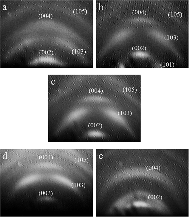
Figure 1. The RHEED patterns of InN (0002) plane films at various N2 flux for (a) 60 sccm, (b) 70 sccm, (c) 80 sccm, (d) 90 sccm, and (e) 100 sccm, respectively.
XRD Analysis
After the experiment was over, the InN thin film samples prepared for different nitrogen flow rates were characterized by XRD to reveal their crystallization properties. Figure 2 shows that the lattice orientations 43.9° and 75.4° correspond to the (111) and (220) diffraction peaks of the self-supporting diamond substrate. The highest diffraction peak at 31.3° in Figure 2 is the diffraction peak of the prepared InN thin film and corresponds to the diffraction peak of InN (002). The XRD pattern shows that the InN thin film samples prepared on the self-supporting diamond substrate have an excellent preferred orientation: The film material grows perpendicularly to the substrate, and a high c-axis preferred orientation is achieved. The analysis of the XRD pattern reveals that the InN thin film samples prepared in this study have excellent crystallization properties. The effect of the nitrogen flow on the crystallization properties of the thin film samples was further studied. The following equation can be derived from Scherrer's formula:
where d is the size of the crystal grains, λ is the wavelength of the Cu Kα rays and is equal to 0.15406 nm, θ is the Bragg diffraction angle, and B is the half-peak width of the film. The measured degrees of the c-axis diffraction peaks, the half-peak widths, the crystal grain sizes, and the c-axis lattice constants of the InN thin film samples prepared under different nitrogen flow rates as well as the calculated stress of each thin film sample are listed in Table 1. When the nitrogen flow rate increases from 60 to 80 sccm, the c-axis lattice constant of the prepared film gradually decreases, the crystal grain size gradually increases, and the FWHM gradually decreases. When the nitrogen flow rate further increases from 80 to 100 sccm, the c-axis lattice constant gradually increases, the crystal grain size gradually decreases, and the FWHM gradually increases. The results show that the film sample prepared under a nitrogen flow rate of 80 sccm has a larger crystal grain size and a smaller FWHM. This can be explained in the following way: The InN thin film samples are prepared by using the ECR-PEMOCVD system, and the nitrogen reaction source is nitrogen gas. During the preparation process, the nitrogen molecules are difficult to ionize, and they decompose because the nitrogen gas is an inert gas. When the nitrogen flow rate is low, the insufficient nitrogen decomposition keeps the supply of the nitrogen reaction source at a low level, resulting in a large number of nitrogen vacancies. Consequently, the reaction with trimethylindium is not sufficient. Therefore, a large number of indium particles are present, leading to the poor crystallization quality of the prepared thin film samples. As the nitrogen flow rate continues to increase, the efficiency of the N2 ionization reaction improves, producing more nitrogen ions. However, because not enough indium reacts with the nitrogen ions at this time, the quality of the prepared film deteriorates. The analysis shows that the InN film samples prepared at a nitrogen flow rate of 80 sccm have excellent crystallization properties. This is consistent with the results of the RHEED analysis.
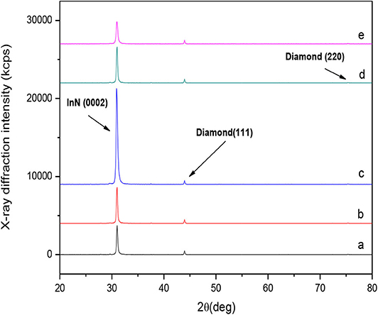
Figure 2. The XRD patterns of InN (0002) plane films at various N2 flux for (a) 60 sccm, (b) 70 sccm, (c) 80 sccm, (d) 90 sccm, and (e) 100 sccm, respectively.
Table 1. The InN (0002) diffraction peak position, FWHM, lattice parameter of c-axis, and grain size.
SEM Analysis
Considering that the lattice constant of the prepared InN thin film differs significantly from that of the self-supporting diamond substrate, the InN film samples prepared on the self-supporting diamond substrate were tested via SEM and analyzed. The test results show that, as the nitrogen flow rate increases from 60 to 80 sccm, the surface island density of the prepared InN film increases, and grain boundaries are clearly visible. As the nitrogen flow rate increases, the competitive growth mechanism of “large islands annexing small islands” takes place, and the island growth mode gradually triggers the layer-island hybrid growth mode. Figure 3 shows that the grain boundaries of the thin film samples prepared under a nitrogen flow rate of 80 sccm tend to become larger, the number of grain boundaries reduces significantly, and the grain boundaries become more stable. The deposited atoms are stacked onto the surface of the substrate in coherent and semi-coherent forms, and the film always spreads out along the surface of the substrate in a two-dimensional expansion mode, showing an excellent layered growth mode. However, as the nitrogen flow rate continues to increase from 80 to 100 sccm, the surface island density of the prepared InN film decreases, the crystal grains become disordered, and the grain boundaries become blurred. As the nitrogen flow rate further increases, the island growth mode of “large islands annexing small islands” does not appear. However, the layer-island hybrid growth mode gradually triggers the d island growth mode. The explanation for this growth mode is the following: In the initial stage of the film formation, some gaseous atoms/molecules begin to condense onto the surface of the substrate, thus initiating the nucleation process. When the gaseous atoms reach the surface of the substrate, the atoms adhere to the substrate at first, and then aggregate to form uniform, fine, and mobile atomic clusters called “islands.” These small bead-like islands continue to accept new deposited atoms and merge with other islands to form bigger islands. The number of islands quickly reaches its saturation level. Although the islands continue to merge, new islands emerge in the vacant areas of the substrate surface. The formation and merging of such small islands take place continuously, and larger islands constantly annex adjacent smaller islands. With the progressing of such phenomenon, the isolated islands are interconnected and form a big piece, and only some isolated holes and channels are left. These holes and channels are continuously filled, forming an initial film with a continuous morphology and a complete coverage.
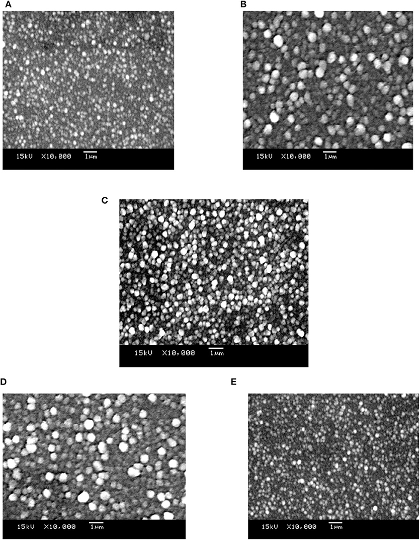
Figure 3. The SEM patterns of InN films at various N2 flux for (A) 60 sccm, (B) 70 sccm, (C) 80 sccm, (D) 90 sccm, and (E) 100 sccm, respectively.
In order to further study the morphology of the InN thin film samples prepared under a nitrogen flow rate of 80 sccm, these thin film samples were tested via SEM once again with a precision of 100 nm. As can be seen from Figure 4, the grain boundaries of the prepared samples are clearly visible, and the crystal grains densely arrange with the same nucleation direction, indicative of an excellent preferential orientation. This analysis result is consistent with the XRD analysis result.
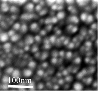
Figure 4. The SEM patterns of InN films at N2 flux with 80 sccm.
AFM Analysis of the InN Thin Films
By considering that the lattice constant of the prepared InN thin film samples differs significantly from that of a self-supporting diamond substrate, the surface morphology of the InN thin film samples prepared on a self-supporting diamond substrate was analyzed by using the AFM method. To pave the way for the subsequent development of optoelectronic devices based on InN thin films, the surface flatness of the InN thin films needs to be on the order of nanometers. The test result shown in Figure 5 indicates that the surface roughness of the prepared InN thin film samples is 3 nm, which fully meets the requirements of the devices concerning the surface flatness. A further analysis of the AFM pattern reveals that when the nitrogen flow rate is 80 sccm, the surface island density of the prepared InN film increases, and the crystal grain boundaries are clearly visible, forming a uniform two-dimensional plane.
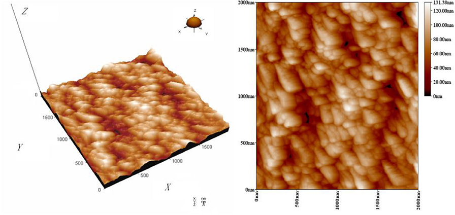
Figure 5. The AFM patterns of InN films at N2 flux with 80 sccm.
EPMA Analysis
The above analysis shows that the prepared films have excellent crystallization properties and surface morphology when the nitrogen source flow rate is 80 sccm. To study the composition of the prepared thin film, the thin film samples were analyzed via EPMA. It can be seen from Figure 6 and Table 2 that, as the nitrogen flow rate increases from 60 to 80 sccm, the In:N atomic ratio of the prepared InN films gradually increases. Actually, the In:N atomic ratio should be 1:1 given the chemical composition of InN. However, when the nitrogen flow rate continues to increase from 80 to 100 sccm, the In:N atomic ratio of the prepared InN film gradually decreases. When the flow rate of the N2 source is 80 sccm, the In:N atomic ratio of the prepared InN thin film sample is 0.88, which is the highest value. This indicates that several nitrogen atoms escape in the process of the thin film growth, which results in a large number of nitrogen vacancies and in an incomplete reaction. The generation of nitrogen vacancies leads to the formation of indium particles, which leads to the formation of metal indium droplets. In this case, the In:N atomic ratio is not close to 1:1.
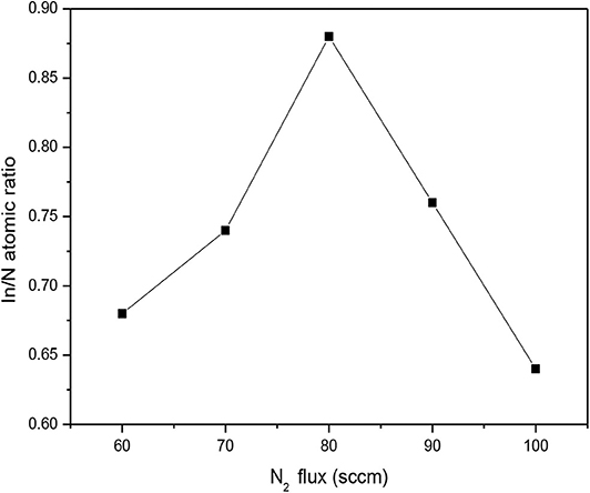
Figure 6. The EPMA patterns of InN films at N2 flux with 80 sccm.
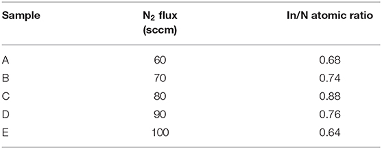
Table 2. The content of InN films deposited at different N2 flux.
Conclusion
A number of InN film samples with superb properties were prepared on a self-supporting diamond substrate under different nitrogen flows using an ECR-PEMOCVD system. The experimental results show that the variation in the nitrogen flow has a great impact on the preferential growth of the (0002) crystal plane of the InN thin film. By increasing the nitrogen flow moderately, the crystal quality of the film can be improved. With an appropriate nitrogen flow, InN thin films with a high c-axis preferential orientation can be obtained, and their surface thin film is relatively flat. However, a too high nitrogen flow does not improve the crystallization quality of the thin films. The EPMA analysis shows that the In:N atomic ratio of the prepared InN film samples is close to 1:1 and that a small amount of metal indium droplets are present. The results of the experiment and of the analysis show that InN thin films prepared under a nitrogen flow rate of 80 sccm have excellent preferential orientation, surface morphology, and atomic ratio.
Data Availability Statement
The original contributions presented in the study are included in the article/supplementary materials, further inquiries can be directed to the corresponding authors.
Author Contributions
SW: the total master planning and film preparation. FQ: experimental data analysis. YB: theoretical study of different test results. DZ: film structure test and analysis.
Funding
This work was supported by the National Natural Science Foundation of China under Grant No. 51872036, the fund of Science and Technology Project of Liaoning, China under Grant No. 20180510049.
Conflict of Interest
The authors declare that the research was conducted in the absence of any commercial or financial relationships that could be construed as a potential conflict of interest.
References
Akasaka, T., Schied, M., and Kumakura, K. (2018). N-face (0001) GaN/InN/GaN double heterostructures emitting near-infrared photoluminescence grown by metalorganic vapor phase epitaxy. Appl. Phys. Exp. 8:081001. doi: 10.7567/APEX.11.081001
Anjum, F., Ahmad, R., and Afzal, N. (2018). Characterization of InN films prepared using magnetron sputtering at variable power. Mater. Lett. 219, 23–28. doi: 10.1016/j.matlet.2018.02.058
Bashir, U., Hassan, Z., and Ahmed, N. (2018). Structural, electrical and optical properties of sputtered-grown InN films on ZnO buffered silicon, bulk GaN, quartz and sapphire substrates. J. Electr. Mater. 8, 4875–4881. doi: 10.1007/s11664-018-6386-3
Bi, Z., Ek, M., and Stankevic, T. (2018). Self-assembled InN quantum dots on side facets of GaN nanowires. J. Appl. Phys. 16:164302. doi: 10.1063/1.5022756
Buzynin, Y., Khrykin, O., and Yunin, P. (2018). InN layers grown by MOCVD on a-Plane Al2O3. Phys. Status Solidi. 11:1700919. doi: 10.1002/pssa.201700919
Darakchieva, V., Xie, M., and Rogalla, D. (2011). Free electron properties and hydrogen in InN grown by MOVPE. Phys. Status Solidi. 208, 1179–1182. doi: 10.1002/pssa.201001151
Dwivedi, S., Ghosh, A., and Ghadi, H. (2018). Oblique angle deposited InN quantum dots array for infrared detection. J. Alloys Compound. 25, 297–304. doi: 10.1016/j.jallcom.2018.06.346
Ke, W., Chiang, C., and Son, W. (2018). InGaN-based light-emitting diodes grown on various aspect ratios of concave nanopattern sapphire substrate. Appl. Surface Sci. 456, 967–972. doi: 10.1016/j.apsusc.2018.06.223
Kobayashi, A., Oseki, M., and Ohta, J. (2018). Epitaxial growth of thick polar and semipolar inn films on yttria-stabilized zirconia using pulsed sputtering deposition. Phys. Status Solidi 255:1700320. doi: 10.1002/pssb.201700320
Liu, H., Wang, X., and Chen, Z. (2018). High-electron-mobility InN epilayers grown on silicon substrate. Appl. Phys. Lett. 112:162102. doi: 10.1063/1.5017153
Lucarelli, G., and Brown, T. M. (2019). Development of highly bendable transparent window electrodes based on MoOx, SnO2, and Au dielectric/metal/dielectric stacks: application to indium tin Oxide (ITO)-free perovskite solar cells. Front. Mater. 6:310. doi: 10.3389/fmats.2019.00310
Madapu, K., and Dhara, S. (2018). Surface-enhanced raman spectroscopy using 2D plasmons of InN nanostructures. Appl. Phys. A. 6:435. doi: 10.1007/s00339-018-1845-5
Madapu, K., Sivadasan, A., and Baral, M. (2018). Observation of surface plasmon polaritons in 2D electron gas of surface electron accumulation in InN nanostructures, Nanotechnology 27:275707. doi: 10.1088/1361-6528/aabe60
Marikutsa, A., Rumyantseva, M., Gaskov, A., Batuk, M., Hadermann J,Sarmadian, N., Saniz, R., et al. (2019). Effect of zinc oxide modification by indium oxide on microstructure, adsorbed surface species, and sensitivity to CO. Front. Mater. 6:43. doi: 10.3389/fmats.2019.00043
Peng, H., Feng, X., and Gong, J. (2018). Low temperature growth of polycrystalline InN films on non-crystalline substrates by plasma-enhanced atomic layer deposition. Appl. Surf. Sci. 30, 830–834. doi: 10.1016/j.apsusc.2018.08.093
Pereira, H. J., and Hatton, R. A. (2019). High figure-of-merit transparent copper–zinc oxide window electrodes for organic photovoltaics. Front. Mater. 6:228. doi: 10.3389/fmats.2019.00228
Polanco, C., and Lindsay, L. (2018). Thermal conductivity of InN with point defects from first principles. Phys. Rev. 98:014306. doi: 10.1103/PhysRevB.98.014306
Qi, K., Lv, W., Iltaf, K., and Liu, S. (2020a). Photocatalytic H2 generation via CoP quantum-dot-modified g-C3N4 from electroless plating. Chin. J. Catal. 41, 114–121. doi: 10.1016/S1872-2067(19)63459-5
Qi, K., Xie, Y., Wang, R., Liu, S., and Zhao, Z. (2019). Electroless plating Ni-P cocatalyst decorated g-C3N4 with enhanced photocatalytic water splitting for H2 generation. Appl. Surf. Sci. 466, 847–853. doi: 10.1016/j.apsusc.2018.10.037
Qi, K., Xing, X., Amir, Z., Li, M., Wang, Q., Liu, S., et al. (2020b). Transition metal doped ZnO nanoparticles with enhanced photocatalytic and antibacterial performances: experimental and DFT studies. Ceramics Int. 46, 1494–1502. doi: 10.1016/j.ceramint.2019.09.116
Tharsika, T., Thanihaichelvan, M., Haseeb, A. S. M. A., and Akbar, S. A. (2019). Highly sensitive and selective ethanol sensor based on ZnO nanorod on SnO2 thin film fabricated by spray pyrolysis. Front. Mater. 6:122. doi: 10.3389/fmats.2019.00122
Yu, Q., Rong, P., Ren, S., Jiang, L., and Li, Y. (2019). Fabrication and electrochemical performance of Al-Doped ZnO nanosheets on graphene-based flexible substrates. Front. Mater. 6:208. doi: 10.3389/fmats.2019.00208
Zhang, D., Qin, F., Bai, Y., and Bian, J. (2012). Effect of buffer layer on the structural and morphological properties of GaN films grown with ECR-PEMOCVD. Diamond Related Mater. 21, 88–91. doi: 10.1016/j.diamond.2011.10.016
Keywords: InN thin film, nitrogen flow, self-supporting diamond substrate, ECR-PEMOCVD, low temperature
Citation: Wang S, Qin F, Bai Y and Zhang D (2020) Study on Preparation and Properties of InN Films on Self-Supporting Diamond Substrates Under Different Nitrogen Flows. Front. Mater. 7:154. doi: 10.3389/fmats.2020.00154
Received: 31 March 2020; Accepted: 29 April 2020;
Published: 10 June 2020.
Edited by:
Kezhen Qi, Shenyang Normal University, ChinaReviewed by:
Guoqiang Liu, Northeastern University, ChinaChunqiang Zhuang, Beijing University of Technology, China
Copyright © 2020 Wang, Qin, Bai and Zhang. This is an open-access article distributed under the terms of the Creative Commons Attribution License (CC BY). The use, distribution or reproduction in other forums is permitted, provided the original author(s) and the copyright owner(s) are credited and that the original publication in this journal is cited, in accordance with accepted academic practice. No use, distribution or reproduction is permitted which does not comply with these terms.
*Correspondence: Fuwen Qin, qfw@dlut.edu.cn