Pin-Hole-Free, Homogeneous, Pure CsPbBr3 Films on Flat Substrates by Simple Spin-Coating Modification
 Satyajit Gupta
 Michael Kulbak
 David Cahen
- 1Department of Materials & Interfaces Weizmann Institute of Science, Rehovot, Israel
- 2Department of Chemistry, Indian Institute of Technology Bhilai, Chhattisgarh, India
We show a simple modification of spin-coating to obtain pinhole-free, well-covering and uniform films of an all-inorganic Pb-halide perovskite (Pb-HaP), on a flat substrate (i.e., not mesoporous) at standard temperature and pressure. In Pb-HaP-based devices the active film is generally fabricated by spin-coating. This is a challenging task for purely inorganic Pb-HaPs, as, except if nano-crystallites can be used, mostly rough and inhomogeneous thin films with poor optoelectronic quality are obtained. We describe a gas flow-assisted method to fabricate thin conformal films of phase-pure CsPbBr3. First cells made with the resulting CsPbBr3-films, yield solar conversion efficiencies up to 2.5%. Electron beam-induced current measurements of device cross-sections show uniform charge generation profiles, implying ≥ ~ 0.2 μm diffusion lengths. Non-encapsulated devices generate stable photocurrent for > 1 hr under continuous illumination at maximum power in ambient.
Introduction
Lead-based halide perovskites (HaPs) with stoichiometry AMX3 (where A is a monovalent organic cation such as methylammonium–MA+; M is a divalent metal cation-Pb2+ and X is a monovalent anion, a halide, iodide–I−, bromide–Br− or chloride–Cl−) have evolved as an important class of semiconducting materials for optoelectronics, due to their excellent optical and electronic properties (Hodes, 2013; Stranks et al., 2013; Yin et al., 2014; Saliba et al., 2016; Yang et al., 2017). With some specific AMX3 compositions photovoltaic energy conversion efficiencies close to 25% were demonstrated recently1. We focus on bromide-based HaPs (with ~ 2.3 eV band gap, EG), as they exhibit high open-circuit voltage (VOC) (Edri et al., 2013, 2014; Kedem et al., 2015; Kulbak et al., 2015, 2016), which makes them attractive starting materials for tandem cells as partner with c-Si ones. Bromide based halide perovskites have been used for high performance photodetector application (Zeng et al., 2018). CsPbBr3 is a broad band-gap material (EBG= 2.32 eV). Such materials are less studied than the smaller bandgap ones and methods to synthesize them are limited. Importantly, solar cells or light-emitting devices, made with such perovskites generate high open circuit voltage/ green-blue emission. High voltage solar cells are of interest for use in tandem or spectral splitting systems. While the bandgap of pure CsPbBr3 is higher than optimal for use in tandem cells, understanding and optimizing fabrication of the more optimal mixed bromide/iodide analogs requires studying and understanding the parent compounds. Pure CsPbBr3 is of direct interest for solar energy conversion, and storage as chemical energy (in chemical bonds) through water splitting and CO2 reduction. Hence, studies of CsPbBr3 are of direct importance for energy conversion and storage.
In previous work we have shown that if caesium (Cs+) is used as A cation instead of MA in the HaP, used to make the solar cell, not only are efficiencies similar to those of hybrid MAPbBr3-based cells, but solar cell stability is better than for MAPbBr3-based cells under prolonged AM1.5 illumination (Kulbak et al., 2016). However, preparing CsPbBr3 films that are
• phase-pure (i.e., are composed of only the perovskite with ABX3 stoichiometry),
• continuous, pinhole-free and, thus, cover, completely also flat, non-mesoporous substrates,
• smooth (absence of randomly oriented irregular shaped crystallites with RMS roughness of < ~10 nm)
is a challenging task.
Indeed, most devices use a mesoporous oxide substrate to get acceptable films. For studying many of the material's fundamental properties for optoelectronic applications, a smooth, continuous well-covering thin film on a regular substrate is preferred or, at times, even needed. In this work we adapted a gas flow-assisted method, earlier used for organic-inorganic hybrid HaPs (Yu et al., 2018), to deposit such CsPbBr3 films on a surface that is not mesoporous but flat. The flow of gas (through a nozzle) during spin-coating retards, due to rapid cooling by solvent evaporation, growth of nuclei, increasing the density of nucleation sites, thus helping to make the film that grows more uniform. Our focus in this preliminary study was to explore a new method to produce phase-pure and pinhole-free CsPbBr3, which was attained by the method, discussed in the work. Preliminary results of the performance of first solar cells, prepared with such CsPbBr3 films, are promising. Further work is needed to enhance efficiency of the devices and measurement of their EQE and EIS, which will be our future studies.
Results and Discussions
The process of the gas flow-assisted method is shown in Scheme 1, in which the perovskite precursor solution is dropped over the substrate and then the spinning is started. During spinning, gas is blown from the top surface, resulting in the uniform film formation.
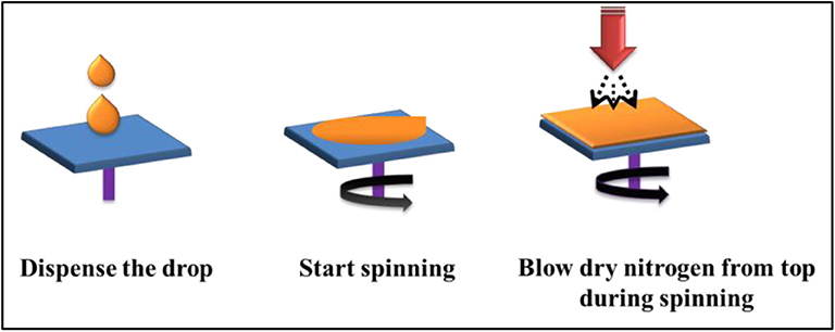
Scheme 1. N2 gas flow—assisted method for fabrication of pinhole-free CsPbBr3 thin films.
Figure 1A shows the absorption spectrum of the ~200 nm thick CsPbBr3 films, deposited over ~70 nm dense TiO2 (d-TiO2), coated on fluorine-doped tin oxide (FTO). The onset of absorption corresponds to, EG, of 2.32 eV, consistent with earlier reports. The photoluminescence (PL) emission peak of CsPbBr3 (deposited on a bare glass substrate) is at 530 nm (Figure 1A). The XRD pattern shows no evidence of different Cs-Pb-Br or Pb-Br or Cs-Br phases, i.e., within the accuracy of this method, phase-pure CsPbBr3 formed. XRD pattern of reference CsPbBr3 powder (# 97851 in the ICSD database) is shown in Figure 1B. All peaks in the diffraction patterns of the samples can be identified as belonging to, and indexed for CsPbBr3, plus those from the TiO2 (substrate marked with *), as shown in Figure 1B. Such a result is obtained within a precursor concentration range between 0.4 (M) and 0.45 (M), and after annealing at 250°C for 10 min. For concentrations > 0.45 (M), additional peaks were found (Figure 1B), corresponding to Cs2PbBr6. SEM images show smooth and pinhole-free films on the flat d-TiO2-coated FTO on glass substrate, as can be seen in the cross-section, shown in Figure 1C. The SEM image of the surface of the film is shown in Figure S1.
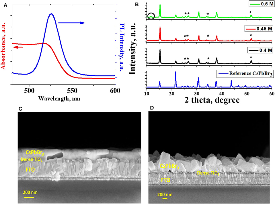
Figure 1. (A) UV-Visible absorption and photoluminescence (PL) spectra of the CsPbBr3 thin film, prepared by the gas flow-assisted process, on dense TiO2-coated FTO on glass, and on glass substrate, respectively, (B) XRD spectra of such CsPbBr3 films on dense TiO2-coated FTO substrate, using different concentrations of salt precursors (“*” represent diffraction peaks from the d-TiO2 substrate) and reference CsPbBr3 powder data (# 97851 in the ICSD database), (C,D) cross-sectional SEM of CsPbBr3 films prepared by gas flow assisted method (C) and prepared by the two-step method (D).
We compared the films of CsPbBr3, grown by gas flow-assisted with those grown by two-step deposition, both on FTO-coated glass slides. Cross-section SEM of the CsPbBr3, fabricated by the two-step deposition technique (Kulbak et al., 2015) over a dense TiO2, i.e., d-TiO2-coated FTO-on-glass slide is shown in Figure 1D (for planar SEM image see SI, Figure S2). The films grown by the two- step method are very inhomogeneous and show irregular crystallites that are oriented rather randomly on the d-TiO2 on the FTO-coated glass substrate. Thus, a mesoporous, mp-TiO2 layer had to be used with the two-step method, to obtain reasonable conversion efficiencies of CsPbBr3 solar cells, made with the two-step process.
Having the CsPbBr3 on a mesoporous substrate, while a practical solution, limits options for using other substrates and above all, the ability to study the HaP itself! In contrast, the gas-flow assisted method produces smooth and pin-hole free films on relatively smooth substrates, such as d-TiO2, and hence mesoporous layer is not necessary for the solar cells. Moreover, XRD revealed that films grown by two-step method are not phase-pure and consist of a mixture of CsPbBr3, CsPb2Br5, and Cs4PbBr6 (Figure S3).
To fabricate cells, CsPbBr3 films (on d-TiO2-coated FTO) were used in an n-i-p configuration, where TiO2 serves as the n-type electron transport layer and poly-triarylamine (PTAA) as the p-type hole transport layer. The device structure was completed by thermal deposition of 100 nm of Au as contact on the PTAA. An SEM image of the cell cross-section is shown in Figure 2B. The cell parameters (open-circuit potential, VOC, short-circuit current density, JSC, fill factor, FF and light-to-electrical power conversion efficiency) were measured using simulated 1 sun illumination (AM1.5), with a solar simulator. The CsPbBr3 device exhibited a PCE of 2.5%. The current density-voltage (J-V) curves of the device (light and dark) are shown in Figure 2A and the device parameters are given in Table S1.
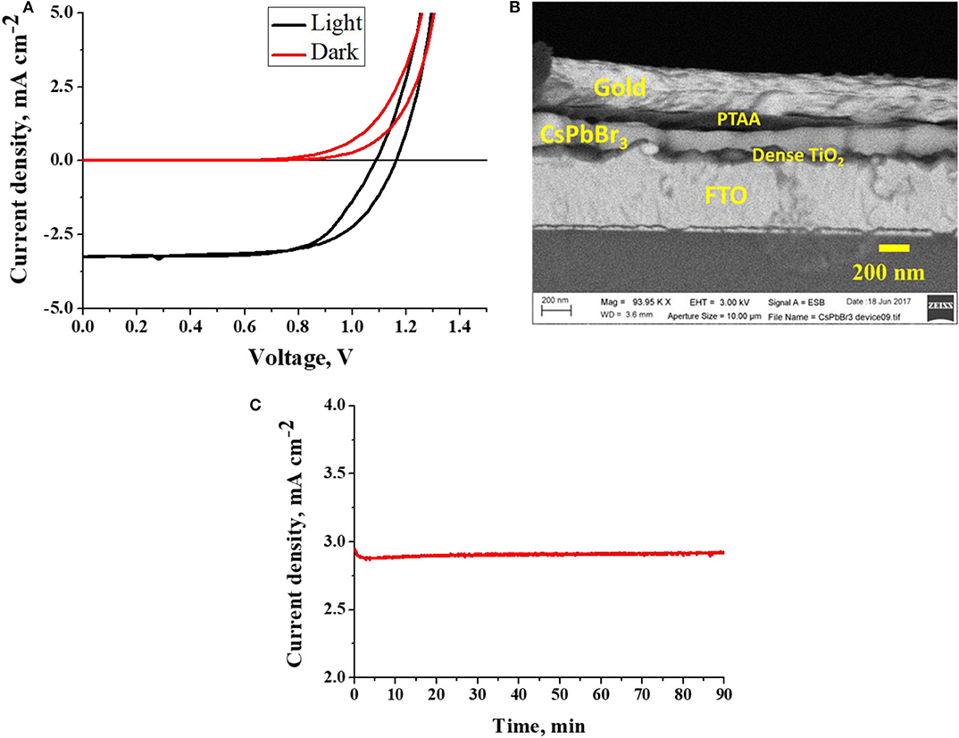
Figure 2. (A) I-V characteristics of CsPbBr3 in the dark and under (~ AM1.5G) illumination, (B) Cross-sectional view of CsPbBr3 device, (C) Photocurrent generation (at maximum power point) from non-encapsulated CsPbBr3 devices under 1 sun illumination for > 1 h, in ambient (air).
We did EBIC analysis on the cross section of the best device to understand the charge generation profile (shown in Figure 3) from various interfaces. It can be observed from Figure 3 that charge generation occurs throughout the CsPbBr3 film. Monte Carlo simulations of electron trajectory estimates that at 3 keV, the vast majority of electrons will reach ~60 nm away from the area of interaction. Thus, charge carrier diffusion lengths must exceed ~80 nm (film thickness minus generation volume diameter), which implies that the EBIC signal is governed by the minority carrier diffusions length, and not by the electron beam-matter volume of interaction. This further testifies to the good quality of the CsPbBr3 films produced by this method.
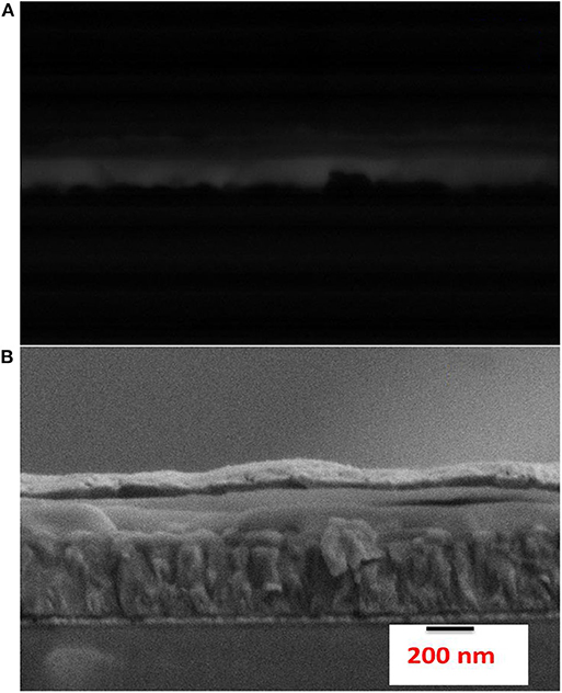
Figure 3. (A) EBIC response from a cross-section of a CsPbBr3 PV device showing a signal through the entire film thickness and (B) the corresponding secondary electron image of the device (cf. to Figure 2B). Because the EBIC signal does not decay within the active material, its thickness sets a lower limit for the carrier diffusion lengths in the film.
The importance of this method can be realized from the extremely simple and non-demanding fabrication route, that lends itself to optimization to produce solar cell quality materials. Furthermore, the stability of the non-encapsulated devices was tracked by keeping these devices at maximum power point under AM1.5 simulated illuminations for 1.5 h (Figure 2C). It can be observed that the non-encapsulated device generated stable photocurrent during the period of illumination. At present we show fair unencapsulated stability, at least comparable to that of CsPbBr3 devices made by other methods. In future study focus will also be on stability of the solar cells as a function of temperature and light illumination. The straightforward way in which a widely used method can be adapted to yield what we describe and exemplify here, makes the information in this short communication is very valuable for researchers that require such thin films for their work, be it academic or applied.
Experimental Section
Device Fabrication
Fluorine (F)-doped tin oxide (FTO)-based transparent conducting substrates (Xinyan Technology TCO-XY15) were cut into specific size and thoroughly cleaned by sonication in warm aqueous alconox solution, deionized water, acetone and ethanol, followed by drying under a N2 stream. After an oxygen plasma treatment, a compact ~60 nm thin TiO2 layer was deposited to the clean substrate by spray pyrolysis of a 30 mM titanium diisopropoxide bis(acetylacetonate) (Sigma Aldrich) solution in isopropanol using air as the carrier gas on a hot plate set to 450°C, followed by a two-step annealing procedure at 160°C and 500°C, each for 1 h in air (Kulbak et al., 2015).
The CsPbBr3 films were prepared by adding a flow nitrogen (N2) stream at a specific stage of the process, as follows:
First the substrates (FTO coated with thin layer of TiO2; substrate size: 2 cm ×2 cm) were etched by oxygen plasma asher for 10 minutes to clean the surface and enhance wettability. Immediately after this treatment, the substrates were placed on the spin-coater. After that, 250 μL of the precursor solution (containing various concentrations of both CsBr and PbBr2, viz. (0.4, 0.45, and 0.5 M) were added to the substrate (FTO coated with thin layer of TiO2) and spin coating was started immediately. The spin -coating was carried out in two consecutive stages. For the first 10 s the spinning speed was 500 RPM, followed by 20 s at 2000 RPM. After 10 sec of spinning (in the second stage), nitrogen gas was blown (at 0.5 LPM-liter per minute) from the top of the spin coater (vertically onto the substrate) for 10 s. The method of film fabrication by gas-flow assisted method was repeated 25–30 times and the results were observed to be consistent from SEM and UV –Visible analysis. Smooth film was observed to appear after the spinning was stopped. The overall procedure was carried out in an ambient atmosphere. For complete device fabrication, poly[bis(4-phenyl) (2,4,6-trimethylphenyl)amine] (PTAA—Lumtec) was deposited by spin-coating 5 s at 500 rpm followed by 40 s at 2000 rpm. For CsPbBr3, the PTAA solution contained 12 mg in 1 mL of chlorobenzene, mixed with 7.5 μL of tert-butylpyridine (TBP) and 7.5 μL of 170 mg/mL LiTFSI [bis(trifluoromethane)sulfonamide (in acetonitrile)]. The samples were left overnight in the dark (under dry air atmosphere) before ~100 nm gold contacts were thermally evaporated through a shadow mask with 0.24 cm2 rectangular holes. For two-step deposition of CsPbBr3 films we used the method, described in earlier studies (Kulbak et al., 2015).
XRD measurements were carried-out on a Rigaku ULTIMA III operated with a Cu anode at 40 kV and 40 mA. The measurements were taken using a Bragg-Brentano configuration through a 10 mm slit, a convergence Soller 5° slit and a “Ni” filter.
Optical transmission and reflection spectra of films were measured using a Jasco V-570 spectrophotometer equipped with an integrating sphere. Transmission was corrected for reflection by using Tcorr = T/(1-R). A Zeiss SUPRA scanning electron microscope was used for SEM and EBIC imaging of the device cross-sections.
The J-V characteristics of the solar-cells were measured with a Keithley 2400-LV SourceMeter and controlled with a Labview-based, in-house written program. A solar simulator (ScienceTech SF-150; with a 300 W Xenon short arc lamp from USHIO Inc., Japan) equipped with an AM1.5 filter and calibrated with a Si solar cell IXOLARTM High Efficiency SolarBIT (IXYS XOB17-12x1) was used for illumination. The devices were characterized through a 0.16 cm2 mask. The J-V characteristics were taken after light soaking for 10 s at open circuit and at a scan rate of 0.06 V/s (unless otherwise stated).
EBIC analysis was done in a Zeiss-Supra SEM using beam current of 5 pA and beam energy of 3 keV (Kulbak et al., 2016). Current was collected and amplified using Stanford Research Systems SR570 pre-amplifier. The device cross section was exposed by mechanical cleaving immediately (up to 2 min) before transferring the sample into the SEM vacuum chamber (10−5 mbar).
Conclusions
In this study, we showed how adding a “gas flow” allows fabricating smooth, pin-hole free, phase-pure thin films of CsPbBr3 on a flat (i.e., not mesoporous) substrate, as shown with the aid of SEM and XRD analysis. Such CsPbBr3 films can be used to make planar architecture solar cells with n-i-p configuration. Non-encapsulated solar cells give, in first experiments, conversion efficiencies up to 2.5% under AM1.5 illuminations and were relatively stable under constant illumination for >1 h.
Data Availability Statement
All datasets generated for this study are included in the article/Supplementary Material.
Author Contributions
SG prepared the films and characterized. MK have performed the EBIC and analyzed the results. DC helped in the preparation of manuscript and evaluation of results.
Conflict of Interest
The authors declare that the research was conducted in the absence of any commercial or financial relationships that could be construed as a potential conflict of interest.
Acknowledgments
We thank Gary Hodes for discussions and Dr. Pallavi Singh for help with the X-ray diffraction data analysis. Partial support for this research work was provided by the Yotam project, via the Weizmann Institute of Science's Sustainability and Energy Research Initiative, SAERI, and by the Israel Ministry of Energy and Infrastructure.
Supplementary Material
The Supplementary Material for this article can be found online at: https://www.frontiersin.org/articles/10.3389/fenrg.2020.00100/full#supplementary-material
Footnotes
References
Edri, E., Kirmayer, S., Cahen, D., and Hodes, G. (2013). High open-circuit voltage solar cells based on organic–inorganic lead bromide perovskite. J. Phys. Chem. Lett. 4, 897–902. doi: 10.1021/jz400348q
Edri, E., Kirmayer, S., Kulbak, M., Hodes, G., and Cahen, D. (2014). Chloride inclusion and hole transport material doping to improve methyl ammonium lead bromide perovskite-based high open-circuit voltage solar cells. J. Phys. Chem. Lett. 5, 429–433. doi: 10.1021/jz402706q
Kedem, N., Brenner, T. M., Kulbak, M., Schaefer, N., Levcenko, S., Levine, I., et al. (2015). light-induced increase of electron diffusion length in a p–n junction type CH3NH3PbBr3 perovskite solar cell. J. Phys. Chem. Lett. 6, 2469–2476. doi: 10.1021/acs.jpclett.5b00889
Kulbak, M., Cahen, D., and Hodes, G. (2015). How important is the organic part of lead halide perovskite photovoltaic cells? Efficient CsPbBr3 cells. J. Phys. Chem. Lett. 6, 2452–2456. doi: 10.1021/acs.jpclett.5b00968
Kulbak, M., Gupta, S., Kedem, N., Levine, I., Bendikov, T., Hodes, G., et al. (2016). Cesium enhances long-term stability of lead bromide perovskite-based solar cells. J. Phys. Chem. Lett. 7, 167–172. doi: 10.1021/acs.jpclett.5b02597
Saliba, M., Matsui, T., Seo, J. Y., Domanski, K., Correa-Baena, J. P., Nazeeruddin, M. K., et al. (2016). Cesium-containing triple cation perovskite solar cells: improved stability, reproducibility and high efficiency. Energy Environ. Sci. 9, 1989–1997. doi: 10.1039/C5EE03874J
Stranks, S. D., Eperon, G. E., Grancini, G., Menelaou, C., Alcocer, M. J. P., Leijtens, T., et al. (2013). Electron-hole diffusion lengths exceeding 1 micrometer in an organometal trihalide perovskite absrober. Science 342, 341–344. doi: 10.1126/science.1243982
Yang, W. S., Park, B. W., Jung, E. H., Jeon, N. J., Kim, Y. C., Lee, D. U., et al. (2017). Iodide management in formamidinium-lead-halide–based perovskite layers for efficient solar cells. Science 356, 1376–1379. doi: 10.1126/science.aan2301
Yin, W. J., Shi, T., and Yan, Y. (2014). Unique properties of halide perovskites as possible origins of the superior solar cell performance. Adv. Mater. 26, 4653–4658. doi: 10.1002/adma.201306281
Yu, M., Huang, X., Shao, J., and Zhang, W. (2018). A novel nitrogen-assisted method for the perovskite active layer optimization in the inverted planar heterojunction perovskite solar cells. IOP Conf. Ser. Mater. Sci. Eng. 446:012004. doi: 10.1088/1757-899X/446/1/012004
Keywords: thin films, solar cell, halide perovskite, stability, electron beam-induced current
Citation: Gupta S, Kulbak M and Cahen D (2020) Pin-Hole-Free, Homogeneous, Pure CsPbBr3 Films on Flat Substrates by Simple Spin-Coating Modification. Front. Energy Res. 8:100. doi: 10.3389/fenrg.2020.00100
Received: 13 October 2019; Accepted: 07 May 2020;
Published: 09 June 2020.
Edited by:
Chunling Wang, Shanghai Jiao Tong University, ChinaReviewed by:
Xiaoming Li, Nanjing University of Science and Technology, ChinaRen Yuan Hang, Fudan University, China
Copyright © 2020 Gupta, Kulbak and Cahen. This is an open-access article distributed under the terms of the Creative Commons Attribution License (CC BY). The use, distribution or reproduction in other forums is permitted, provided the original author(s) and the copyright owner(s) are credited and that the original publication in this journal is cited, in accordance with accepted academic practice. No use, distribution or reproduction is permitted which does not comply with these terms.
*Correspondence: Satyajit Gupta, satyajit@iitbhilai.ac.in