Design of an Open Electrowetting on Dielectric Device Based on Printed Circuit Board by Using a Parafilm M
 Zichuan Yi
 Haoqiang Feng
 Xiaofeng Zhou2
 - 1College of Electron and Information, University of Electronic Science and Technology of China, Zhongshan Institute, Zhongshan, China
- 2South China Academy of Advanced Optoelectronics, South China Normal University, Guangzhou, China
In recent years, the open electrowetting on dielectric (EWOD) device has been widely used in biomedical detection, chemical synthesis analysis, and so on. However, the cost of using ITO glass as surface material is difficult to meet the requirement for large-scale array chip production. So, a low-cost, easy-to-manufacture open EWOD platform is designed in this paper. In hardware platform, an operation platform is prepared by using a printed circuit board (PCB) as a substrate. The electrode shape is designed as zigzag, and its surface is optimized by organic solderability preservatives (OSP). In addition, Parafilm M and silicone oil are used as a dielectric hydrophobic layer to prepare the open platform. In software, the system program is designed by C programming language, including initialization program, serial port communication program, high-voltage output port program, and interrupt program, which can be used to drive droplets. The system can achieve an effective driving voltage of 180–240 V. The moving speed of droplets can reach 15 mm/s when the droplet volume is 1850 μL and the electrode voltage output frequency is 10 Hz.
Introduction
The open EWOD system has the advantages of saving samples, easy integration, multi-function, and precise operation [1–3], and so on. It has been used in many fields and has great development potential. Most of digital microfluidic systems are made on the basis of ITO glass currently [4], and it can realize the smooth movement of droplets, which is favored by the majority of scientific researchers and the market. However, the cost of ITO glass surface material is difficult to meet the needs of large-scale array chip production. It has been reported that a simple ITO glass EWOD device (4.5 × 1.5 cm2) currently costs several hundred dollars [5]. In addition, a gap of several micrometers in width can be etched on the surface of the ITO glass by using a mask, but this means that all traces and electrodes can only be laid out on one side of the glass [6]. So, it has serious limitations on the compatibility and expansibility of devices. Therefore, in order to overcome those shortcomings, PCBs were used to prepare EWOD devices.
With the rapid development of electronics manufacturing industry, the PCB manufacturing industry has a unified and standardized manufacturing facility and process [7]. Moreover, it has the characteristics of low cost and high integration, which is suitable for making EWOD devices [8–10]. In current PCB manufacturing process, a PCB with a thickness of several millimeters can accommodate up to 30 wiring layers. It can achieve electrical performance connection by the via process, which can improve wiring efficiency [11]. So, the PCB has been used as the base of a two-dimensional electrode array to fabricate EWOD devices as early as 2005 [12]. Once this scheme was proposed, many researchers did a lot of design research on PCB-based EWOD devices. However, there are still many shortcomings in the PCB-EWOD devices. For example, a closed PCB-based EWOD device manufacturing method was proposed to drive 1 μL droplet, and the manufacture of a dielectric layer (SU-8) and a hydrophobic layer (Teflon AF1600) on the PCB is completed by chemical vapor deposition (CVD) technology [13]. However, the droplet size is too small, and the closed structure brings inconvenience for droplets replacement. In addition, an open PCB-based EWOD device manufacturing method was proposed, and spin coating technology was used to deposit a layer of polydimethylsiloxane (PDMS) on the electrode, a 6 μL liquid drop can be driven at the voltage of 380 V after adding silicone oil, but the movement speed is only 2.71 mm/s [14]. So, the driving efficiency is low. In order to improve the performance of EWOD devices, a lot of research of electrode shape and material selection for the dielectric layer and the hydrophobic layer have been done [15, 16]. Among them, different electrode shapes (crescent, interdigitated, rectangular, notched, and zigzag edges) have been designed on the EWOD device. The results showed that the zigzag edge can drive droplets more effectively than other types [17]. But the driving voltage must be higher than 300 V for obtaining a droplet speed of 10 mm/s, which can cause the breakdown for general dielectric materials. In addition, a PCB-EWOD device which was produced by a 2 × 4 electrode array has been proposed, polyethylene films, and edible oil were used as dielectric materials. However, the device can only drive a 2.5 μL droplet with a high driving voltage and the number of electrodes was too small to be used in the large-scale manipulation [18].
In this paper, an open EWOD device is proposed based on a PCB, and a kind of zigzag edge is used for the design of electrode shape, Parafilm M film and silicone oil are used as the dielectric hydrophobic layer. The device can realize the driving of large droplets, and reduce costs at the same time. In addition, once the surface of the dielectric material is damaged, it can be torn off and replaced for further use. So, the proposed EWOD device can improve the integration of the system and has a certain cost advantage.
Principle
Electrowetting Principle of Droplets
By adjusting the electric potential applied between the liquid and the electrode, the surface tension is changed, thus the contact angle is changed, which is called as electrowetting phenomenon. As shown in Figure 1A, it is the shape of the droplet when no voltage is applied, and a droplet is tiled as Figure 1B when voltage is applied. Its contact angle can be determined by Young's Equation [19], as shown in Equation (1).
Where, γsg, γsl, γlg are surface tensions of solid-gas, solid-liquid, and liquid-gas, respectively, and θ0 is the initial contact angle of the droplet. For hydrophobic surfaces, the contact angle of discrete droplets is always >90°. The hydrophobic solid-liquid interface tension becomes smaller when the driving voltage U is applied between the electrode and the droplet, and the relationship is described by the Lippmann Equation [20], as shown in Equation (2).
Where, γslU is the surface tension of the solid-liquid interface when the voltage is applied, γsl is the surface tension when the voltage is canceled. ε0 and εr are the dielectric constant in vacuum and the effective dielectric constant of the dielectric layer, respectively, d is the thickness of the dielectric layer. As the interfacial tension of the solid-liquid interface becomes smaller, the contact angle of the droplet becomes smaller, as shown in Figure 1B, the contact angle θU can be derived from (1) and (2), as shown in Equation (3) [21].
In Equation (3), the original contact angle θ0 is a constant, the greater of the applied voltage, the smaller of the contact angle. In addition, the change of the contact angle is related to the dielectric constant and the thickness of the dielectric layer.
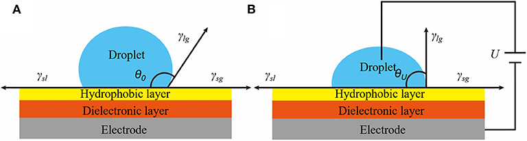
Figure 1. Schematic diagram of the droplet electrowetting. (A) Schematic diagram of a droplet contact angle without voltage application. (B) Schematic diagram of a droplet contact angle when the voltage is applied.
Droplet Movement Principle
The contact angle of a droplet on the electrode could decrease gradually when the voltage applied on the electrode increases gradually. The contact angle between two sides of the droplet will vary greatly when the voltage reaches a certain value. So, a large unbalance force ΔF can be formed in the droplet. When the force is greater than the friction between the droplet and the electrode, the droplet can be driven to one side gradually, which toward the direction of voltage [22]. As shown in Figure 2, and ΔF can be expressed as Equation (4).
Where, γ is the surface tension of the droplet; θ1 is the initial contact angle of the droplet and θ2 is the contact angle when the voltage is applied; C is a constant; ε0 and εr are the dielectric constant of the dielectric layer and the dielectric constant in vacuum, respectively. d is the thickness of the dielectric layer, A is the area of the droplet; U is the driving voltage.
Figure 2. Schematic diagram of droplets moving on two adjacent electrodes. (A) The schematic diagram of a droplet moving toward a charged electrode from a stationary initial state. (B) The schematic diagram of a droplet when it reaches the charged electrode.
Bottom Area Calculation of a Droplet on an EWOD
In order to obtain the relationship between the size of an electrode and the minimum droplet size which can be driven, the volume of a droplet is quantified as the bottom radius of the droplet. The bottom radius of the droplet can be calculated by using the spherical void formula [23], and the corresponding minimum droplet volume can be estimated by comparing with the size of the electrode, as shown in Equation (5).
Where, V is the volume of a droplet, H is the height of the droplet on the EWOD, R is the radius of the droplet. The shape diagram of a droplet on the EWOD is shown in Figure 3. The volume of a droplet can be obtained by using a pipette gun to fill the electrode in each experiment. So, in the static state, the relationship among the bottom radius of the droplet, the radius of the droplet and the contact angle can be calculated, as shown in Equation (6).
Where, r is the radius of a droplet on the bottom of an electrode and α is the contact angle between the droplet and the electrode, and α can be obtained by a contact angle meter. Then, the bottom area S can be calculated as Equation (7).
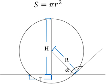
Figure 3. Schematic diagram of the shape of a droplet on the EWOD.
Device Fabrication
Preparation of a PCB-Based Electrode Array
The PCB supports flexible or rigid substrate, and electrode arrays can be fabricated on rigid or flexible substrate. Rigid FR4 has good mechanical and electrical properties, and it is more cost-effective and attractive. In order to develop low-cost and high-compatibility EWOD devices, the rigid FR4 material is used to produce the PCB. Comparison of different materials which can be used to produce the PCB are shown in Supplementary Table 1. The table of detailed information is shown in Supplementary Material.
The edge zigzag is applied to the electrode, as shown in Figure 4A. The electrode surface treatment process is also very important. The electrode surface treatment process has a key impact on the movement of droplets. Electrode treatment processes include: lead tin spraying, lead-free tin spraying, gold deposition, gold plating, OSP and tin deposition, etc. The materials involved include tin, gold and antioxidants. All surface treatment processes are completed on the base copper of the PCB, as shown in Figure 4B. The electrode with different surface treatment has no effect on the electrical performance of PCBs, but its roughness which has a bad effect on droplets movement cannot be ignored. The comparison of electrode surface roughness and price of three common surface treatment processes is shown in Supplementary Table 2. The table of detailed information is shown in Supplementary Material.
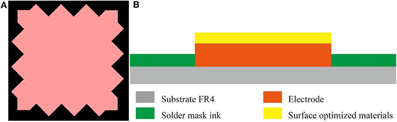
Figure 4. (A) The zigzag electrode schematic diagram, every “tooth” is 500 μm and the depth of “tooth” is 350 μm. (B) Single PCB electrode schematic diagram, and the surface treatment material is covered on electrode.
It can be seen that the surface roughness of the electrode obtained by the lead-free tin spray process is the largest, while the roughness of the immersion gold process and the OSP process is relatively small, so the immersion gold and OSP process are preferred. But OSP has the lowest price, and it is selected for surface treatment process in this paper. The steps for manufacturing PCBs are shown in Figure 5.
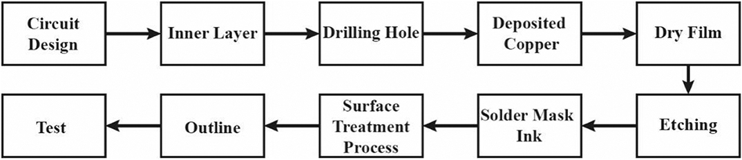
Figure 5. The steps for manufacturing PCBs. There are main ten steps for manufacturing PCBs. Firstly, a correct circuit diagram is generated a Gerber film. According to the diagram, the inner layers are bonded together, the electrical connection is conducted by drilling, the copper is deposited in the hole as the base of electroplated copper, a layer of dry film is pasted on the layout, and the desired pattern can be obtained by etching, and then, the electrode is surface-treated for outline and testing.
According to the design requirements, a zigzag electrode with an electrode size of 2 × 2 mm2 is designed. The number of electrodes is 8 × 8, and an electrode array with a distance between the two electrodes of 140 μm is shown in Figure 6.
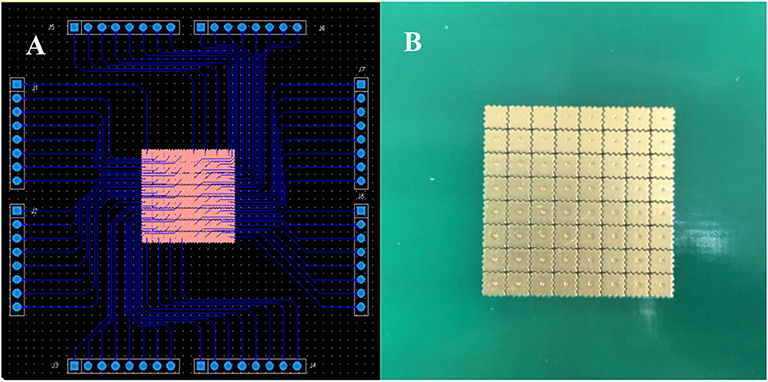
Figure 6. PCB-based EWOD operating platform. (A) The design of a PCB electrode array. (B) The physical picture of the PCB electrode array.
Dielectric Layer
In EWOD devices, the dielectric layer is an important part, which can determine the device performance. At present, the reported dielectric materials used in EWODs are mainly divided into polymer dielectric material and inorganic dielectric material [24]. Because the ITO glass surface is flat. The Teflon can be used for EWODs based on ITO glass by a spin coating process [25].
However, in a standard PCB process, the height difference between the electrodes and the substrate is in the range of 18–70 μm, and the thickness is measured by using an optical microscope. The gap between the two electrodes is 140 μm and the surface roughness of an electrode is about 3.1 μm, which is measured by using a step profiler. The diagram of the two adjacent electrodes is shown in Figure 7. Surface defects can reduce the fluidity of droplets, but the dielectric layer made by ordinary spin coating process cannot fill this huge height difference, and then, the movement of the droplet can be blocked, which could make the EWOD device unusable. So, the Parafilm M is used to realize a “bridge” between two adjacent electrodes, so as to eliminate the influence of the “huge” gap between electrodes in the droplet movement process. The electrowetting performance of a Parafilm M is shown in Figure 8. It can be seen that the contact angle change of a Parafilm M is 43° in the voltage range of 0–340V, and it can be increased with the increase of driving voltage. So, the Parafilm M can produce enough contact angle changes to drive the droplets. Its parameters are shown in Supplementary Table 3, The table of detailed information is shown in Supplementary Material. The initial contact angle of the Parafilm M is more than 90° before and after stretching, which shows hydrophobicity. And the Parafilm M after stretching is used as the dielectric layer by us.
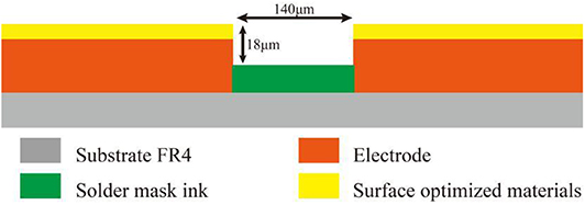
Figure 7. Schematic diagram of two adjacent electrodes on a PCB-based EWOD.
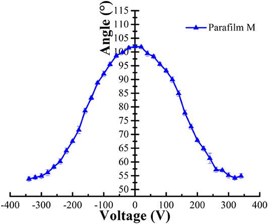
Figure 8. Electrowetting characteristic curve of the Parafilm M.
Results and Discussion
Hardware Design of the Driving System
According to the principle of the electrowetting, the driving system is designed to achieve the manipulation of micro-droplets, the driver board is shown in Figure 9. The driver board can accept an input voltage of 5–250 V. It has 16 editable high-voltage outputs without setting output circuits. In addition, a built-in protection circuit and a short-circuit detection section are designed in the driver. Compared with a driving circuit using a large number of relays and logic components [26], the proposed driving system is simple. As shown in Figure 9, ➀ is the control IC which is the core part of the driving system and a STM32 single-chip is used as the main chip. Its core model is Cortex-M3 and it can run up to 72 MHz. ➁ is a driving module, which mainly consists of a HV513 chip developed by Supertax company and some external circuits. Its function is to provide high output voltage for driving droplets. The HV513 chip can output the external power supply voltage in parallel according to the program, and it can output high resistance state at all ports. At the same time, it can control the output voltage within the range of 5–250 V, and has the function of short circuit automatic monitoring. ➂ is a burning module, which uses ST-LINK V2 simulation programmer to burn the program into STM32 chip; ➃ is a function serial port module, which can use DuPont line to connect two or more driver boards for achieving instruction transfer; ➄ is a power module, a PSW800-1.44 DC power supply is used to drive the system. ➅ is a high-level output port module, which is connected to the EWOD device to provide a high-level voltage. The driving system has two sets of communication serial ports, which are used for the connection between the systems. The maximum communication rate of the system can reach 4.5 Mbps.
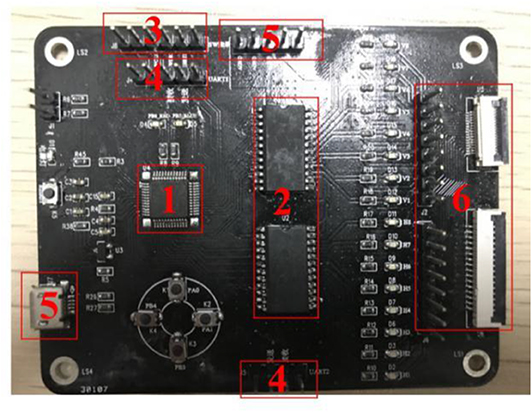
Figure 9. Driving system hardware physical picture.
Design of Software for EWODs
The completion of the hardware circuit provides a basis for the software system. In order to accurately control the movement of droplets, the software system flowchart is shown in Figure 10.
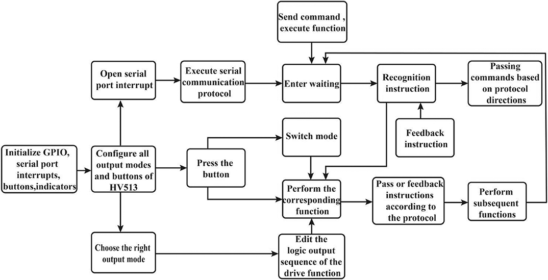
Figure 10. System software flow chart. Each function is in the original standby state, and then, the system starts to configure the output mode of the HV513, which can be divided into three ways to execute the function. The first is to directly execute the original output sequence to complete the corresponding functions. The second is to switch to other output sequences by switching mode keys to perform corresponding functions. The third is to execute the serial program to perform the corresponding functions.
In system initialization, the port parameters and function initialization settings of each module must be configured in the system, including the initial configuration of GPIOs, communication serial ports, interrupts, and so on.
In order to control the movement of droplets, the output logic sequence of the high-voltage port of the system must be set. So, we initialize the function serial port, then configure the output mode, edit the logic output sequence, and output the driving voltage finally. The specific procedure steps are shown in Figure 11.
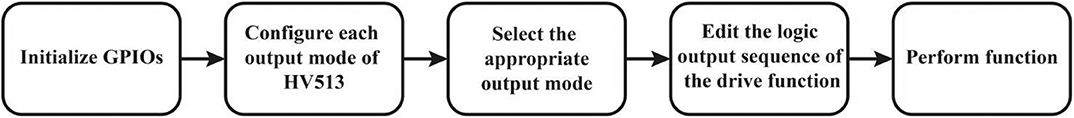
Figure 11. High-voltage parallel output function sequence.
Performance Testing
In order to achieve a smooth movement of droplets, a layer of silicone oil is added on the Parafilm M, whose organic groups are methyl. Methyl silicone oil has good chemical stability, insulation, and good hydrophobic properties. Then, a pipette gun is used to suck up 3 μL of silicone oil and drip it right in the middle of the electrode array, then, the whole device is left for 5 min in a dust-free box to ensure that the silicone oil is spread evenly. The entire EWOD system connection is shown in Figure 12. This system consists of four driving boards and an EWOD platform which are connected by wires. The four driving boards provide the driving voltage for the operation platform by the communication interconnection, and the output sequence of the driving voltage can be adjusted by programming in the STM32. Any one driver board can send completion signal to another driver board when its own instructions are completed. Then, the next driver board can continue to send instructions in order. The system has a total of 64 output voltage terminals which can drive all electrodes in the EWOD. In the process of the operation, STM32 output an instruction signal to a HV513 chip according to the program code, and then, the HV513 can output the high voltage to control the droplet movement on the EWOD device by executing the received command signal.
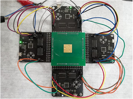
Figure 12. Connection diagram of the EWOD system.
In the testing process, the control variable method is used for obtaining the relationship between the driving voltage and the droplet moving speed with the same droplet volume, and the relationship between the droplet volume and the moving velocity with the same driving voltage.
Firstly, we only changed the driving voltage and tested the relationship between driving voltage and droplet moving speed. As shown in Figure 13A, the output frequency of the electrode driving voltage which refers to the inverse time of two adjacent electrodes is 5 Hz, a 25 μL droplet can be driven to 6.32 mm/s when the driving voltage is >150 V. Then, the droplet velocity can be increased when the voltage is gradually increased. And the droplet moving speed can reach 15.03 mm/s when the driving voltage is 240 V. In addition, the movement stability of the droplets is high during the experiment, and there is no phenomena such as droplet stop, sideslip loss and so on. So, the effective driving voltage of the EWOD device is within 150–240 V, and the speed of a droplet can be increased with the increase of the driving voltage. And then, a fixed driving voltage of 240 V is applied, the size of different droplet volumes and different electrode output frequencies are adjusted, and the droplet volume-velocity relationship curve of the Parafilm M is shown in Figure 13B.
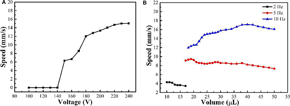
Figure 13. Device performance testing. (A) when the droplet volume is 25 μL, and the dielectric hydrophobic layer is Parafilm M & silicone oil, the relationship between the driving voltage and the droplet moving speed. (B) When the driving voltage is 240 V, the relationship between the droplet volume and the droplet moving speed.
The curve in Figure 13B is measured at three different frequencies. It can be seen that the higher the frequency of the output voltage is, the greater the average moving speed of the droplets is when the droplet volume is the same as each other. Because of a low frequency, a droplet moved to the second electrode, and the third electrode has not yet been applied driving voltage, so the droplet can stay on the second electrode, resulting in “stuck” phenomenon, as shown in Figure 14. However, the droplet has no time to contact the third electrode if the frequency is too high, and the voltage has been switched to the fourth electrode at this time, then, the droplet is “lost.” As shown in Figure 15, a droplet with a volume of 15 μL can be driven normally at a frequency of 2 Hz, but it cannot be driven continuously at a frequency of 5 Hz.
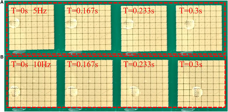
Figure 14. Position comparison of droplets which have the same volume during the driving process when switching frequencies between two adjacent electrodes are 5 and 10 Hz. (A) When the electrode switching frequency is 5 Hz, the droplet is driven from the initial position to the third electrode after 0.3 s. (B) When the electrode switching time is 10 Hz, the droplet is driven from the initial position to the fourth electrode after 0.3 s.
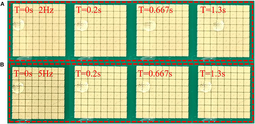
Figure 15. When the droplet volume is 15 μL, the comparison chart of droplets when the electrode switching frequency are 2 and 5 Hz. (A) The droplet moved to the fourth electrode from the initial position after 1.3 s when the electrode switching frequency is 2 Hz. (B) The droplet has no movement from the initial position after 1.3 s when the electrode switching frequency is 5 Hz.
The continuous driving of the droplet cannot be realized when the droplet volume is <10 μL (electrode size is 2 × 2 mm2), no matter how much the driving output frequency is. This is because the bottom area of the droplet is less than the electrode area, and the droplet cannot always contact the next electrode during the moving process, so the droplet cannot move continuously. When the output frequency is 10 Hz and the droplet volume is >18 μL, the droplet velocity can be increased with the volume increase of the droplet, and the velocity can be decreased until the droplet volume is >40 μL. The main reason is that the 240 V voltage can provide enough driving force to the 18–40 μL droplets. As the volume is increased, the effective contact area between the droplet and the electrode also can be increased, so the droplet can obtain a greater driving force. However, the driving force provided by the 240 V is not enough to drive the droplet when the volume is increased to a certain extent, and then, the velocity of the droplet could be decreased. In order to improve the driving speed, the driving voltage and output frequency must be increased at the same time. In summary, the EWOD prepared in this paper can drive the droplets of 40 μL at the driving voltage of 240 V with an output frequency of 10 Hz, and the moving speed of the droplet can reach 16 mm/s.
Conclusion
An EWOD digital microfluidic operating platform based on the PCB which is convenient in manufacture is proposed in this paper, the Paraflim M and silicone oil are used as the dielectric hydrophobic layer for low cost production, and a driver board composed of STM32 and HV513 chips are designed as the control system. Then, the EWOD device can drive large droplets, and the using of removable media material can eliminate cross contamination and expand chip compatibility. So, the proposed EWOD system not only has simple preparation steps, but also reduces production cost, which has a certain practical value.
Data Availability Statement
All datasets presented in this study are included in the article/Supplementary Material.
Author Contributions
ZY and LS designed this project. HF and XZ carried out most of the experiments and data analysis.
Funding
This research was funded by the Guangdong Basic and Applied Basic Research Foundation (no. 2020A1515010420), the Key Research Platforms and Research Projects in Universities and Colleges of Guangdong Provincial Department of Education (no. 2018KQNCX334), the Zhongshan Innovative Research Team Program (no. 180809162197886), the Zhongshan Institute high-level talent scientific research startup fund project (no. 416YKQ04), the Project for Innovation Team of Guangdong University (no. 2018KCXTD033), and the National Key R&D Program of China (no. 2018YFB0407100-02).
Conflict of Interest
The authors declare that the research was conducted in the absence of any commercial or financial relationships that could be construed as a potential conflict of interest.
The reviewer FC declared a shared affiliation with one of the authors, ZY, to the handling editor at time of review.
Supplementary Material
The Supplementary Material for this article can be found online at: https://www.frontiersin.org/articles/10.3389/fphy.2020.00193/full#supplementary-material
References
1. Samiei E, Tabrizian M, Hoorfar M. A review of digital microfluidics as portable platforms for lab-on a-chip applications. Lab Chip. (2016) 16:2376–96. doi: 10.1039/C6LC00387G
2. Decrop D, Ruiz E, Kumar PT, Tripodi L, Kokalj T, Lammertyn J. Digital microfluidics assisted sealing of individual magnetic particles in femtoliter-sized reaction wells for single-molecule detection. Methods Mol Biol. (2017) 1547:85–101. doi: 10.1007/978-1-4939-6734-6_7
3. Torabinia M, Asgari P, Dakarapu US, Jeon J, Moon H. On-chip organic synthesis enabled by engine-and-cargo in an electrowetting-on-dielectric digital microfluidic device. Lab Chip. (2019) 19:3054–64. doi: 10.1039/C9LC00428A
4. Shen HH, Fan SK, Kim CJ, Yao DJ. EWOD microfluidic systems for biomedical applications. Microfluidics Nanofluidics. (2014) 16:965–87. doi: 10.1007/s10404-014-1386-y
5. Moschou D, Tserepi A. The lab-on-PCB approach: tackling the μTAS commercial upscaling bottleneck. Lab Chip. (2017) 17:1388–450. doi: 10.1039/C7LC00121E
6. Abdelgawad M, Wheeler AR. Low-cost, rapid-prototyping of digital microfluidics devices. Microfluidics Nanofluidics. (2008) 4:349–55. doi: 10.1007/s10404-007-0190-3
7. Meimandi A, Seyedsadrkhani N, Jahanshaki A. Development of an electrowetting digital microfluidics platform using low-cost materials. In: 2019 27th Iranian Conference on Electrical Engineering (ICEE). Yazd: IEEE (2019). doi: 10.1109/IranianCEE.2019.8786395
8. Zou FX, Ruan QY, Lin XY, Zhang MX, Song YL, Zhou LJ, et al. Rapid, real-time chemiluminescent detection of dna mutation based on digital microfluidics and pyrosequencing. Biosensors Bioelectron. (2018) 126:551–7. doi: 10.1016/j.bios.2018.09.092
9. Jain V, Raj TP, Deshmukh R, Patrikar R. Design, fabrication and characterization of low cost printed circuit board based ewod device for digital microfluidics applications. Microsyst Technol. (2015) 23:389–97. doi: 10.1007/s00542-015-2680-7
10. Jain V, Vasavi D, Rajendra P. Study of two-dimensional open EWOD system using printed circuit board technology. Global J Res Eng. (2017) 17:59–66.
11. Alistar M, Pop P. Towards droplet size-aware biochemical application compilation for AM-EWOD biochips. In: Symposium on Design IEEE. (2015). doi: 10.1109/DTIP.2015.7161024
12. Gong M, Kim CJ. Two-dimensional digital microfluidic system by multilayer printed circuit board. Micro electro mechanical systems. In: 2005 18th IEEE International Conference on Micro Electro Mechanical Systems. Miami Beach, FL: IEEE (2005).
13. Macro N, Nicola L, Pablo RL, Domenico C, Giampiero DC, Augusto N. 2-D digital microfluidic system for droplet handling using printed circuit board technology. In: 2015 XVIII AISEM Annual Conference. Trento: IEEE (2015).
14. Jain V, Hole A, Deshmukh R, Patrikar R. Dynamic capacitive sensing of droplet parameters in a low-cost open ewod system. Sens Actuators A: Phys. (2017) 263:224–33. doi: 10.1016/j.sna.2017.06.014
15. Jang LS, Hsu CY, Chen CH. Effect of electrode geometry on performance of ewod device driven by battery-based system. Biomed Microdevices. (2009) 11:1029–36. doi: 10.1007/s10544-009-9320-x
16. Xu XW, Sun LN, Chen LG, Zhou ZZ, Xiao JJ, Zhang YL. Electrowetting on dielectric device with crescent electrodes for reliable and low-voltage droplet manipulation. Biomicrofluidics. (2014) 8:064107. doi: 10.1063/1.4902554
17. Jain V, Hole A, Deshmukh R, Patrikar R. Effect of electrode geometry on droplet velocity in open EWOD based device for digital microflfluidics applications. J Electrostatics. (2017) 87:11–8. doi: 10.1016/j.elstat.2017.02.006
18. Zulkepli SNIS, Hamid NH, Shukla V. A low cost open droplet-based microfluidic decvices on printed circuit board. In: 2017 7th IEEE International Conference on Control System, Computing and Engineering (ICCSCE). Penang: IEEE (2017). doi: 10.1109/ICCSCE.2017.8284405
19. Yamaguchi Y, Kusudo H, Surblys D, Omori T, Kikugawa G. Interpretation of Young's equation for a liquid droplet on a flat and smooth solid surface: mechanical and thermodynamic routes with a simple Lennard-Jones liquid. J Chem Phys. (2019) 150:044701. doi: 10.1063/1.5053881
20. Wang J, Zhang J, Liu S. The accurate control of the La2O3 hierarchical structure of the flower-like microspheres accompanied with vertical-standing nanopetals and the electrowetting responses with low voltage actuation. Ceramics Int. (2020) 46:607. doi: 10.1016/j.ceramint.2020.01.147
21. Dreyer W, Guhlke C, Landstorfer M, Muller R. New insights on the interfacial tension of electrochemical interfaces and the lippmann equation. Eur J Appl Math. (2018) 29:708–53. doi: 10.1017/S0956792517000341
22. Gong J, Kim CJ. Direct-referencing two-dimensional-array digital microfluidics using multilayer printed circuit board. J Microelectromechanical Syst. (2008) 17:257–64. doi: 10.1109/JMEMS.2007.912698
23. Abdelgawad M, Park P, Wheeler AR. Optimization of device geometry in single-plate digital microfluidics. J Appl Phys. (2009) 105:094506. doi: 10.1063/1.3117216
24. Liu H, Dharmatilleke S, Maurya DK, Tay AAO. Dielectric materials for electrowetting-on-dielectric actuation. Microsyst Technol. (2009) 16:449–60. doi: 10.1007/s00542-009-0933-z
25. Chao JP. An Q. Liu Z P. Electrowetting on liquid-infused membrane for flexible and reliable digital droplet manipulation and application. Sens Actuators B: Chem. (2019) 291:470–7. doi: 10.1016/j.snb.2019.04.102
Keywords: electrowetting on dielectric, printed circuit board, Parafilm M, dielectric hydrophobic layer, open platform
Citation: Yi Z, Feng H, Zhou X and Shui L (2020) Design of an Open Electrowetting on Dielectric Device Based on Printed Circuit Board by Using a Parafilm M. Front. Phys. 8:193. doi: 10.3389/fphy.2020.00193
Received: 29 March 2020; Accepted: 30 April 2020;
Published: 03 June 2020.
Edited by:
Mohamed Swillam, American University in Cairo, EgyptReviewed by:
Feng Chi, University of Electronic Science and Technology of China, ChinaYong Deng, Dalian University of Technology, China
Ji-Pei Chen, Guangzhou University, China
Copyright © 2020 Yi, Feng, Zhou and Shui. This is an open-access article distributed under the terms of the Creative Commons Attribution License (CC BY). The use, distribution or reproduction in other forums is permitted, provided the original author(s) and the copyright owner(s) are credited and that the original publication in this journal is cited, in accordance with accepted academic practice. No use, distribution or reproduction is permitted which does not comply with these terms.
*Correspondence: Lingling Shui, shuill@m.scnu.edu.cn