High Temperature Conductive Stability of Indium Tin Oxide Films
 Haiou Li
  Xingpeng Liu
 Tangyou Sun
 Fabi Zhang
- Guangxi Key Laboratory of Precision Navigation Technology and Application, Guilin University of Electronic Technology, Guilin, China
Indium tin oxide (ITO) has been studied for applications at normal high temperatures, below 600°C, due to its excellent electrical characteristics. In an attempt to further match the needs of electronics for use in extremely harsh environments, the changes in the conductive properties of ITO films and their mechanism were investigated at special high-temperatures above 1,000°C. ITO films were prepared by pulsed laser deposition (PLD) onto lanthanum gallium silicate (LGS) substrates. Furthermore, the as-deposited samples were annealed with different temperature-time treatments, and we investigated the effects of annealing on the electrical, structure, surface morphology and chemical properties of the ITO films by X-ray diffraction analysis, scanning electron microscopy (SEM), resistance measurements, and X-ray photoelectron spectroscopy (XPS). The experimental results showed that the decreased resistance of the ITO films was mainly attributed to the increase in the crystalline size and the increased amount of Sn4+ ions during the heating period (0–1,000°C). Generally, the ITO films showed stable electrical properties when they were heated at 1,000°C for at least 2.5 h. As expected, the ITO films that remained steady above 1,000°C have potential applications as electrodes working in special high-temperature environments.
Introduction
Tin-doped indium oxide (ITO), which possesses good electrical conductivity, high optical transparency in the visible light range and a wide optical band gap, is a kind of important transparent conducting oxide (Adurodija et al., 1999; Granqvist and Hultåker, 2002; Chung et al., 2005; Kato et al., 2011; Song et al., 2011; Reddy et al., 2017). ITO films have been widely used as transparent conductors in numerous devices such as thin-film solar cells (Toušková et al., 1995; Kanneboina et al., 2018), liquid crystal displays (LCDs) (Sawada et al., 2001), organic light-emitting devices (Kim et al., 1999), antistatic conductive films, sensors, and for automotive applications (Granqvist and Hultåker, 2002; Meshram et al., 2015; Ke et al., 2016; Sun et al., 2016; Ahmed et al., 2019). ITO thin films have been produced using several techniques that include: RF magnetron sputtering (Canhola et al., 2005), chemical vapor deposition (CVD) (Park et al., 2002), electron beam evaporation (Diniz, 2011), ion beam-assisted deposition (ISD) (Yang et al., 2004), pulsed laser ablation (PLA) (Adurodija et al., 1999, 2005), and dip coating (Nishio et al., 1996).
With the increasing demand for electronic products that are stable at high temperatures, the need for conductive materials that operate stably at high temperatures has also risen accordingly. However, the efficiency of relevant electronic devices has been limited by the unstable electrical resistivity of the materials at extremely high-temperatures. ITO thin films show a good electrical conductivity and can operate at high temperatures. Additionally, ITO films also exhibits excellent optical performance. Based on the above mentioned advantages, ITO films have been widely used in a variety of fields for applications such as strain sensors, temperature sensors, and thermoelectric devices (Gregory et al., 2002; Kato et al., 2011; Meshram et al., 2015; Sun et al., 2016; Liu et al., 2017; Premkumar and Vadivel, 2017; Zhang et al., 2017; Liu and Peng, 2018). But the conductive property of ITO films for applications above 1,000°C has been rarely studied, which restricts research into related high-temperature devices. So, it is necessary to investigate the conductive mechanism of ITO films at 1,000°C, providing a theoretical foundation for enhancing its conductive stability at such high temperatures in the future.
The majority of literature focuses on analyzing the electrical and optical properties of ITO thin films at normal high temperatures (Liu and Zuo, 2010; Diniz, 2011; Sun et al., 2016; Reddy et al., 2017; Qin et al., 2018). Hence in this paper, we have fabricated ITO films onto lanthanum gallium silicate (La3Ga5SiO14, LGS) substrates and systematically discussed the role of microstructure and the chemical composition on the electrical properties of these films by XRD, SEM, and XPS analysis. In order to further report the electrical performance of ITO materials, the as-deposited ITO samples underwent successive annealing steps from room temperature (25°C) to 1,100°C in air. The main focus of this work was to study rules and principles of the conductivity changes in ITO films at temperatures ranging from 25 to 1,000°C, thus determining the potential of ITO films themselves as an electrode at special high-temperatures.
Experimental Details
ITO films were 100 nm thick and were deposited onto LGS substrates by a KrF excimer laser (Lambda Physics Compex 201, 248 nm, and FWHM of 25 ns) at a fluence of 3 J/cm2 and frequency of 3 Hz. Before deposition, the LGS substrate was first ultrasonically cleaned in acetone and anhydrous alcohol for 5 min each. Then, these cleaned LGS substrates were dried by N2 and transferred into the deposition chamber. Next, the substrates were heated to about 500°C before deposition. The PLD system was pumped to a base pressure of 5 × 10⁻⁴ Pa and the 100 nm thick ITO films were prepared in the 20 Pa flowing oxygen pressure. Details of the PLD system used to grow ITO films are mentioned elsewhere (Adurodija et al., 1999, 2005).
The microstructure of the ITO films was observed by using Field-Emission Scanning Electron Microscopy (FE-SEM) (JSM-IT500HR). The electrical properties were performed using a four-point probe and the Hall Effect Measurement (van der Pauw method) technique (ECOPIA, HMS-3000). In addition, the real-time resistance (Rs) was measured by a combination of a Keithley 2400 source meter and a small box furnace (KSL-1200X-J) at different temperatures. The film thickness was measured with a stylus profile meter (KLA Tencor P-10 surface profiler). The chemical analysis of the films was observed with X-ray Photoelectron Spectroscopy (XPS) with Al Kα radiation (hν1/41486.6 eV). Figure 1 shows the transmittance and absorbance spectra of the as-deposited ITO films at wavelengths between 200 and 800 nm. The optical bandgap of the as-deposited films range from 3.3 ± 0.02 eV to 3.5 ± 0.02 eV, which is consistent with reported results (Premkumar and Vadivel, 2017).
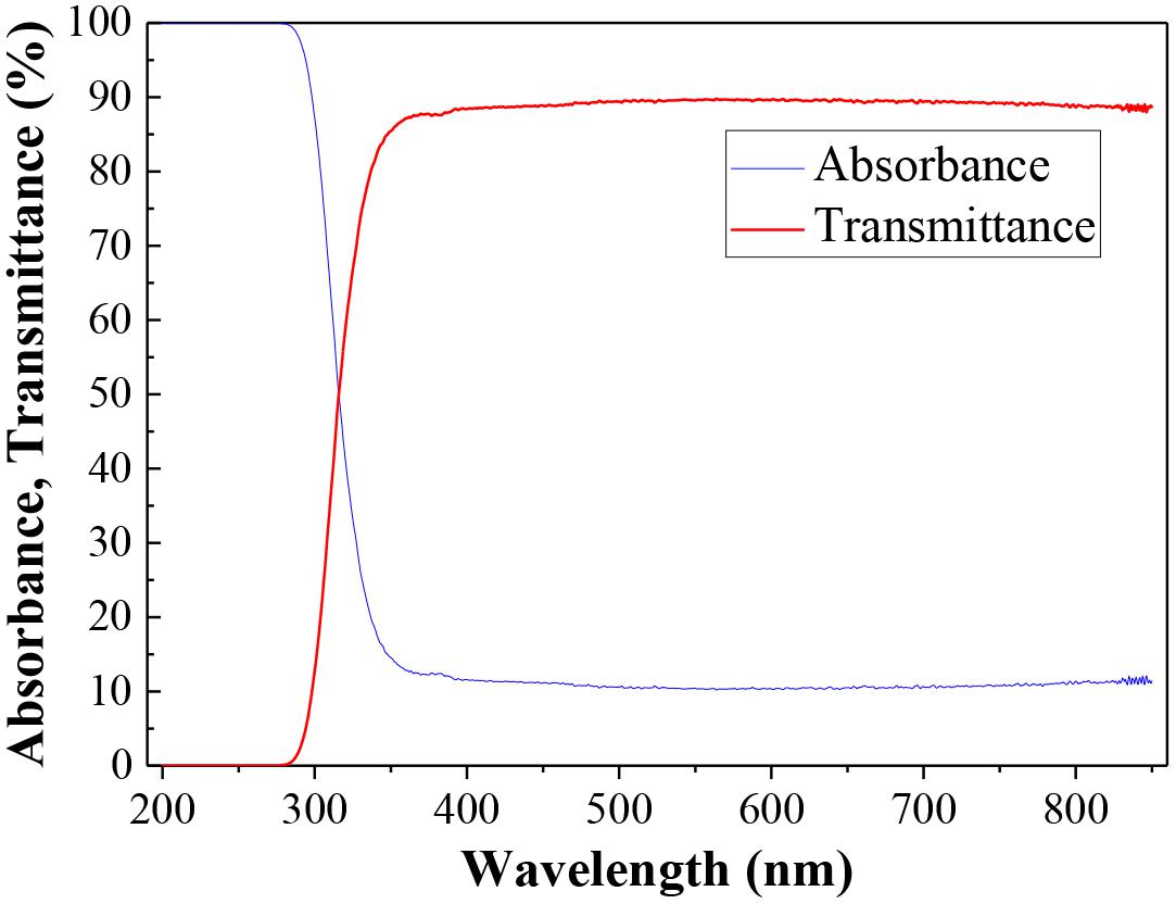
Figure 1. Optical transmittance and absorbance spectra of as-deposited ITO films.
Results and Discussion
Electrical Conductivity of ITO Films During Heating-Up and Holding Stage
Figure 2 shows the resistance of ITO films grown on LGS substrates influenced by annealing temperature and time in air. In Figure 2A, Rrt means the resistance of the ITO films at room temperature and ΔR represents the difference between the resistances at room temperature and annealing temperature. It can be seen that the resistance of ITO films is affected greatly by the annealing temperature. With the annealing temperature increasing from 25 to 150°C, the resistance of ITO films does not vary. As the temperature keeps rising, the resistance then exhibits a 0.3-fold decrease from 150 to 700°C, whereas it presents a 0.4-fold decrease from 700 to 950°C. Finally, the resistivity of the ITO films remains almost unchanged when the annealing temperature varies from 950 to 1,100°C.
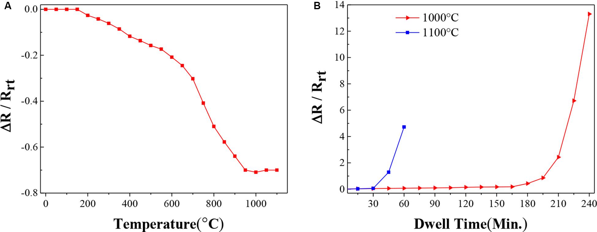
Figure 2. Real-time resistance changes of the ITO films deposited onto LGS substrates as the function of (A) temperature and (B) dwell time at 1,000 and 1,100°C.
Figure 2B presents the real-time resistance change curve of ITO films when they were heated at 1,000°C for varying dwell times. In this figure, ΔR represents the difference between the resistances at 0 h and the specified dwell time. It can be seen that the resistance of ITO films heated at 1,000°C exhibits a slow 0.18-fold increase after 165 min and only exhibits a 0.67-fold increase after 195 min. Then the resistance sharply increases with the passing of time, thereby destroying the conductive properties. In addition, the resistance of the ITO films heated at 1,100°C sharply increases after 30 min, and the conductive property of ITO films is completely destroyed. Next, the changes in the electrical properties of the ITO films will be analyzed after annealing by studying the microstructure and chemical composition of the ITO films.
Effect of Film Microstructure on the Electrical Conductivity
The XRD patterns of the ITO films grown on LGS substrates and annealed at different temperatures in air are shown in Figure 3. Most of the annealed ITO films have a structure with diffraction peaks that correspond to (222), (400), and (622) reflections. This shows that these films consist of polycrystalline ITO grains with a random orientation. Two weaker peaks in the XRD pattern could be identified as the (222) and (400) reflections of the ITO films before the ITO samples were heated. After heating to 400°C and dropping to room temperature, the peaks of the ITO films at the (222) and (400) orientations are significantly enhanced, indicating the preferred orientation of the ITO grains. In the curves of XRD corresponding to annealing temperatures of 700 and 1,000°C, the (400) peak dominates, implying that the crystalline grains in these films are highly oriented along the (400) direction. According to the measured XRD results, it can be seen that (400) is the main orientation of the ITO grains.
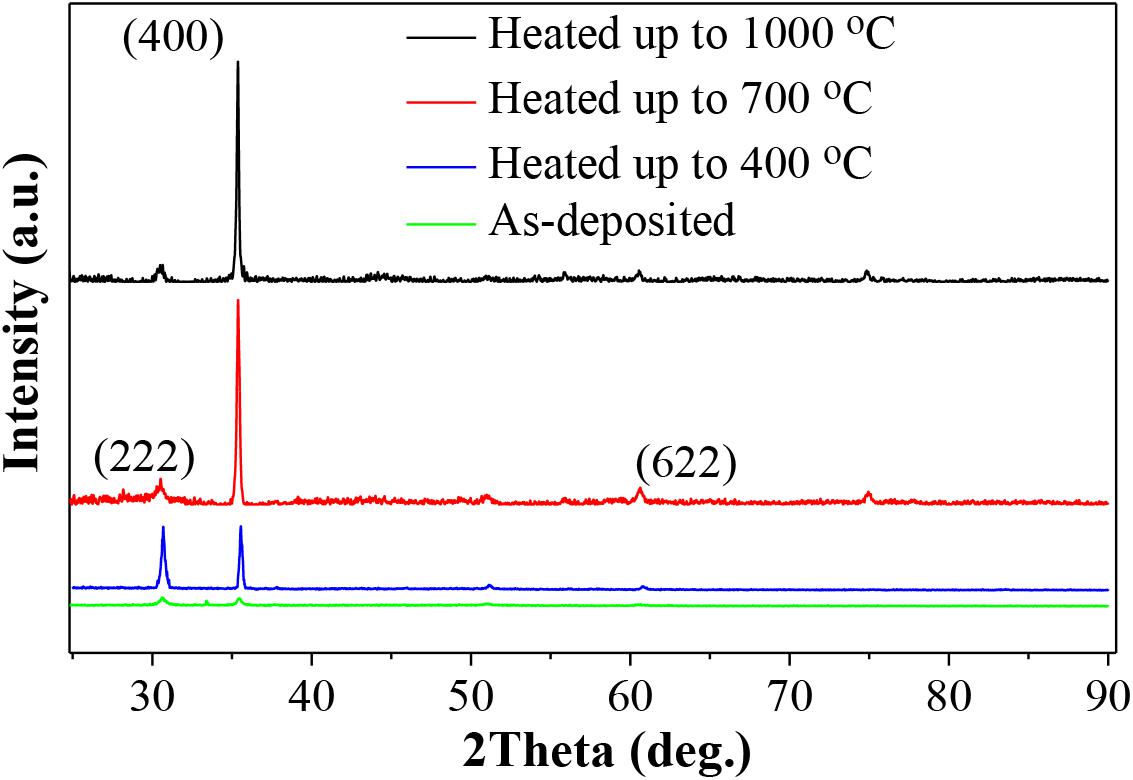
Figure 3. XRD patterns of the ITO films deposited onto LGS substrates, annealed at different temperatures.
Figure 4 shows the effect of holding time on the XRD patterns of ITO films grown on LGS substrates when the dwell time was increased from 1 to 4 h. The majority of ITO films annealed at different dwell times have a structure with strong peaks corresponding to (400) reflections. The results show that the microstructure of ITO films is affected minorly by dwell time when it was heated at 1,000 or 1,100°C.
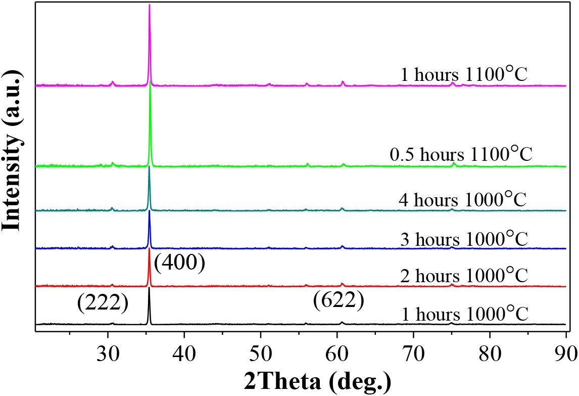
Figure 4. XRD patterns of the ITO films deposited onto LGS substrates, annealed for different dwell times.
Figure 5A shows that the grain size and full width at half maximum (FWHM) of ITO films grown on LGS substrates along the (400) direction as a function of annealing temperature. According to the calculated results, it can be seen that ITO films have an FWHM of 0.3259° and a grain size of 26.16 nm at room temperature. The FWHM of ITO films heated at 400°C greatly decreases to 0.2001°C and the grain sizes greatly increase to 42.61 nm. The FWHM of the thin films also decreases when the annealing temperature increased to 700 and 1,000°C. The grain sizes increase to 48.97 and 52.92 nm, respectively. Additionally, the grain sizes of the ITO films change significantly for the temperature range 20–400°C, further implying that the microstructure of these ITO films undergo a significant change during the beginning of the heating stage.
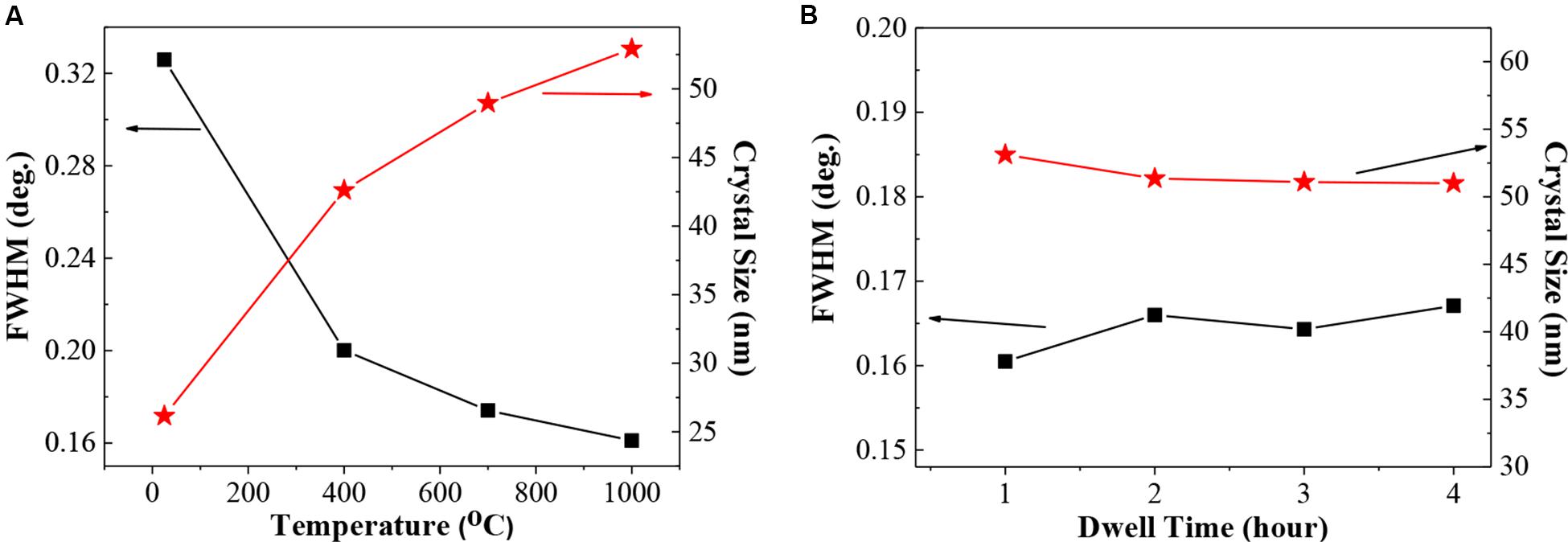
Figure 5. Grain size and Full Width at Half Maximum (FWHM) of the ITO films deposited onto LGS substrate annealed at different (A) temperatures and (B) dwell times at 1,000°C, along the (400) direction.
Figure 5B shows that the grain size and FWHM of the ITO films grown on LGS substrates along the (400) direction as a function of dwell time at 1,000°C. The ITO films have the largest grain sizes when they were heated for 0.5 h at 1,000°C. With increasing dwell time, the grain sizes of the ITO films slowly decrease from 53 to 51 nm, implying that the microstructure of these ITO films remains almost stable for a long time (1–4 h). The results show that the crystalline state of ITO hardly changes as the dwell time increases, indicating that the microstructure of ITO is basically stable at 1,100°C and it will not affect the changes in the conductive properties.
As shown in Table 1, the grain sizes were calculated by X-Ray Diffraction measurements (Ren Xu et al., 2010). The dislocation density and lattice distortion of the ITO films were found to vary from 9.3 × 10⁻⁶ to 6.59 × 10⁻⁵ lines m–2 and from -0.0021 to -0.0598, respectively. The annealed films showed less dislocation density and lattice distortion than that of the as-deposited films during the heating process. Additionally, the dislocation density remains almost stable during the whole heat preservation process, indicating that the film stress has been totally released during the heating process.
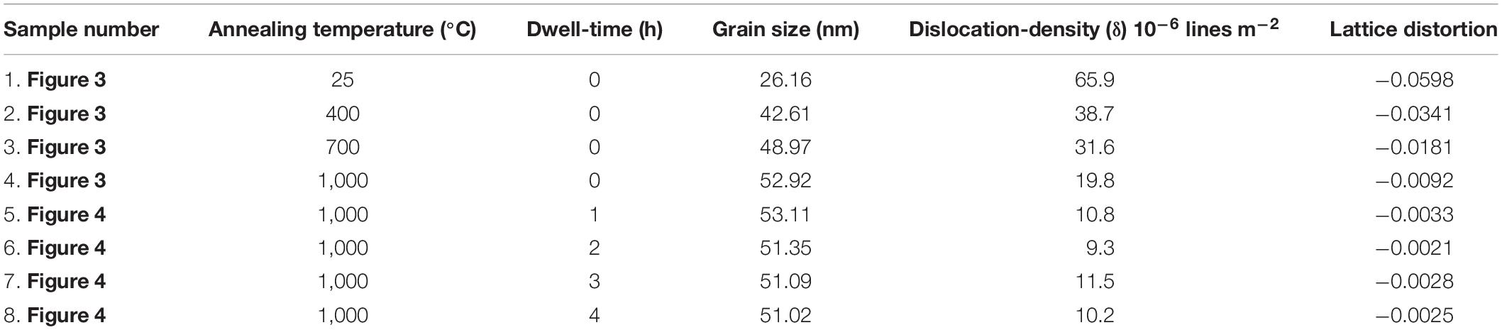
Table 1. Variation of grain size, dislocation density, and lattice distortion for the ITO films.
Figure 6 shows SEM images of the surface morphology of the ITO films annealed at different temperatures and dwell times. As shown in Figures 6A,B, the surface morphology of these films are strongly affected by the annealing temperature. It is obvious that, with an increase in the annealing temperature, the grain sizes become larger, and the distance between grain boundaries become smaller. The grain sizes of the ITO films prepared with annealing temperatures of 25 and 1,000°C obtained from XRD are 26.16 and 52.92 nm, respectively. It is well known that the presence of these gaps has a great influence on the electrical conductivity of ITO films, and that the longer the distance between grain boundaries, the more the electrons will be hindered from passing through the grains, leading to a greater electrical resistivity of the ITO film (Zhao et al., 2017). Therefore, increased grain size and reduced distance between grain boundaries are considered to be two of the reasons that resistance of ITO films decreases.
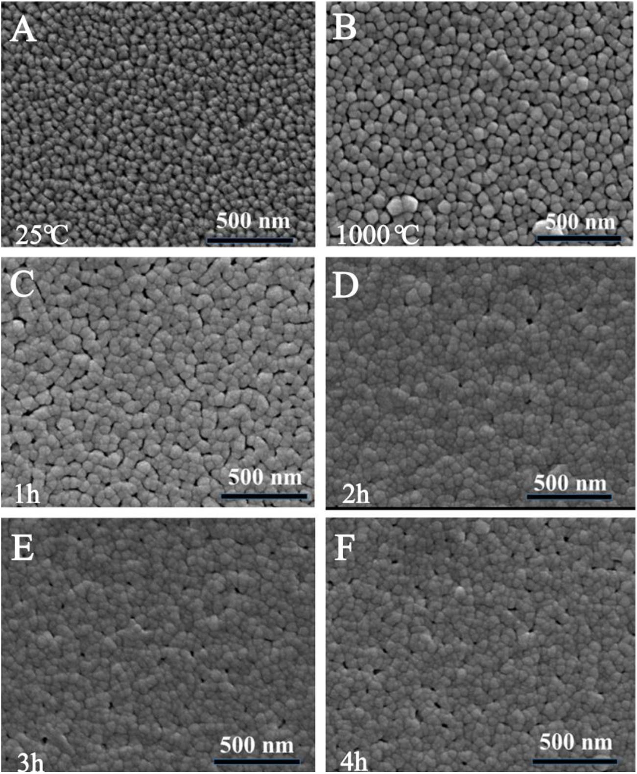
Figure 6. Plane-view SEM images of ITO films at different temperatures (A,B) and dwell times (C–F) heated at 1,000°C.
As shown in Figures 6C–F, the surface morphology of the ITO films annealed at 1,000°C are influenced by dwell time. The grain sizes of the ITO films prepared with an annealing time of 1, 2, 3, and 4 h obtained from XRD are 53.11, 51.35, 51.09, and 51.02 nm, respectively. It is obvious that the distance between grain boundaries of the ITO films are still apparent after 1 h. The distance between grain boundaries of the ITO films decrease obviously when the annealing time is increased to 2 h. The distance between grain boundaries of the ITO film heated at 1,000°C for 3 and 4 h, respectively, can be seen in Figures 6E,F, respectively. The surface morphology is not significantly different from the ITO film heated for 2 h.
In Table 2, the statistical analyses of SEM images were calculated by using ImageJ, and are almost consistent with XRD results. In Figure 6, it can be directly observed that the grains get closer and the grain gaps gradually disappear during the heat treatment process. In addition, after the initial heating process and the first 1 h of the heat preservation process, the surface of the ITO film is found to become smoother as time goes on. After annealing at 1,000°C for 1 h, we can hardly see changes in the surface roughness, indicating that the surface topography tends to be stable.
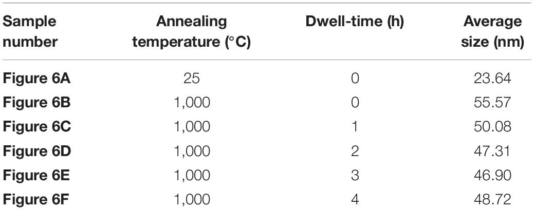
Table 2. Statistical analysis of SEM images.
Based on the results shown above, the distance between grain boundaries has a minimal contribution to the conductivity of ITO films heated at 1,000°C after 2 h. With increasing dwell time, the distance between grain boundaries does not effect the conductivity, implying that the changes in the conductivity of the ITO films is mainly determined by their chemical properties.
Effect of Film Chemical Composition on the Electrical Conductivity
The chemical environment over the surface of the ITO films before and after annealing was investigated by XPS analysis. XPS has been used to examine the chemical binding energies of O1s, In3d, and Sn3d for ITO films on LGS substrates (Diniz, 2011; Zhao et al., 2017; Liu and Peng, 2018).
Figure 7 shows the results of the ITO films which were annealed at 700 and 1,000°C. From Figure 7A, we can see the XPS spectrum of O1s electrons as a function of annealing temperature. It can be seen from the figure that the O1s peak is divided into two independent peaks (Reddy et al., 2017; Qin et al., 2018). The peak with lower binding energy is derived from In2O3 and SnO2 in the fully oxidized state, and the peak with higher binding energy is derived from the oxides of low-valent In and Sn caused by oxygen defects. In addition, the peak area of the XPS spectrum for the Sn4+ ion increases gradually with increasing temperature, as shown in Figure 7B.
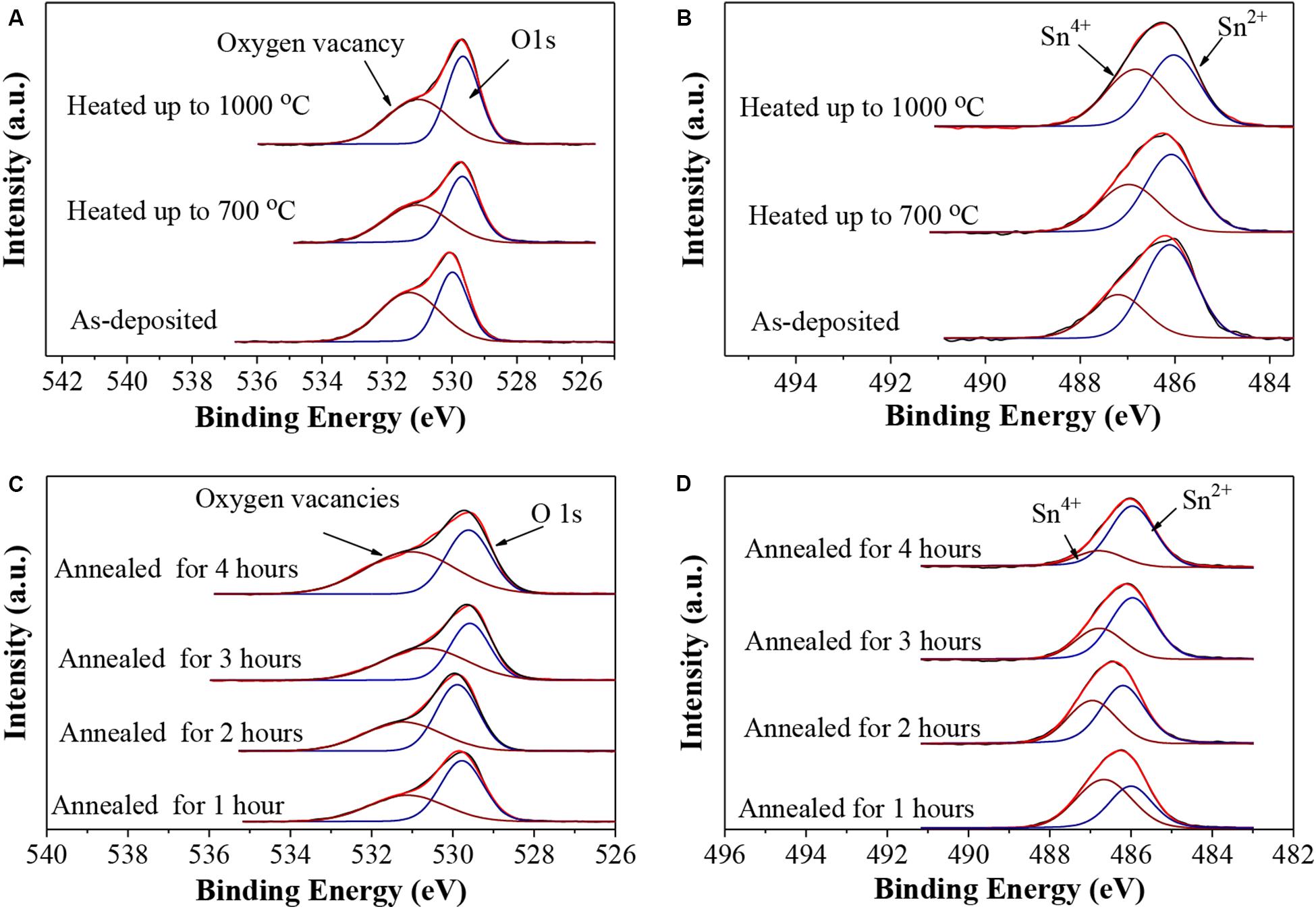
Figure 7. XPS spectra in the O1s, Sn4+, and Sn2+ region for the ITO films annealed at different (A,B) temperatures and (C,D) dwell times, annealed at 1,000°C.
The XPS spectra of O1s and Sn3d electrons of the ITO films heated at 1,000°C for different dwell times are presented in Figures 7C,D. In Figure 7C, with increasing annealing times, the area of the oxygen defect spectrum peak increases, which indicates that the number of oxygen atoms bound to the low-cost In and Sn ions is increasing. This might be due to the gradual decomposition of SnO2 into SnO at a heating-temperature of 1,000°C for a long time, resulting in an increase of oxygen defects (Qin et al., 2018).
Moreover, as shown in Figure 7D, the peak intensity of the Sn4+ ions decreases gradually with increasing annealing temperature, indicating that the Sn4+ ion content also decreases.
Figure 8 illustrates the ratio of Ov to O, and Sn4+ ions to all Sn ions. The Ov and O represent the number of oxygen atoms in the oxygen defect state and all oxygen atoms, respectively. As shown in Figure 8A, with increasing annealing temperature, the ratio of oxygen atoms in the oxygen vacancy state to all oxygen atoms decreases, implying some oxygen vacancies can be effectively filled. The presence of oxygen defects in the ITO films is advantageous for the electrical conductivity of ITO, which is capable of generating electrons to form carriers. Obviously, the ratio of Sn4+ ions to all Sn ions increases from 32.5 to 47.0% with temperature increasing from room temperature to 1,000°C. A large part of the conductivity of ITO is derived from the n-type doping formed by the replacement of In3+ ions by Sn4+ ions. Such enhanced conductivity of ITO films in the heating stage could be due to the decreased number of oxygen defects and the increased amount of Sn4+ ions.
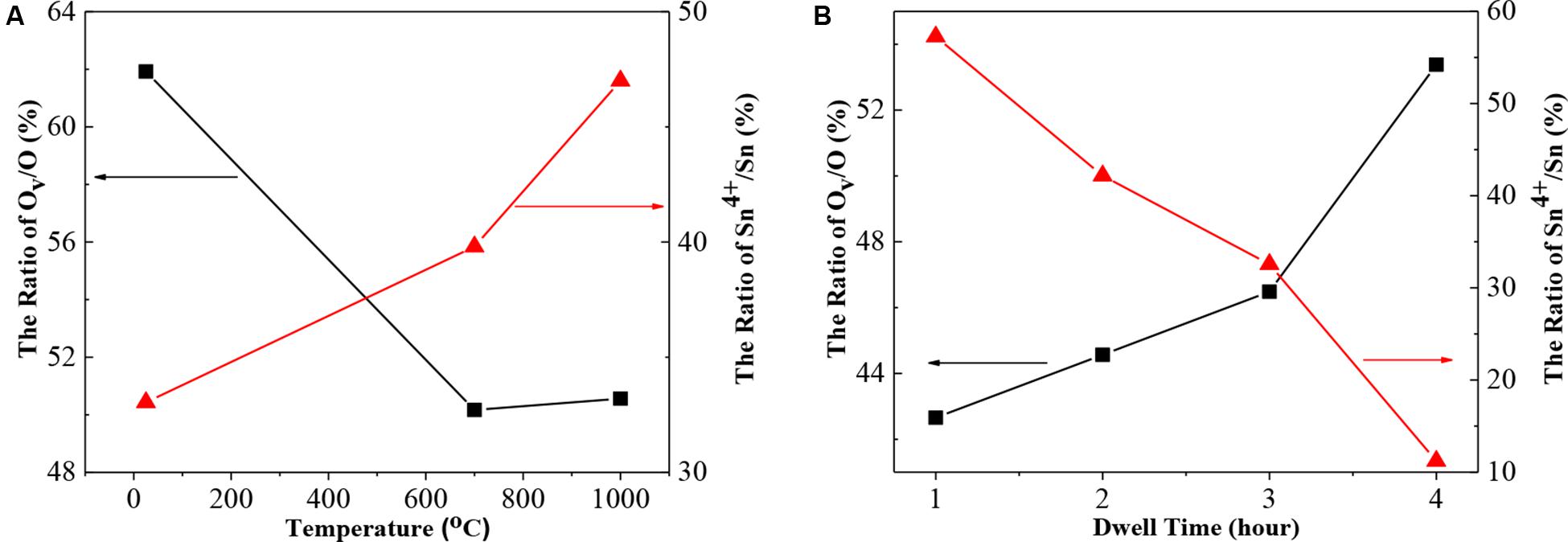
Figure 8. The ratio of Ov/O and Sn4+ of the ITO films presented as a function of (A) temperature and (B) dwell time, heated at 1,000°C.
In addition, the ratio of Sn4+ ions to all Sn ions in the ITO films after heated at 1,000°C for different dwell times is shown in Figure 8B. After heating at 1,000°C for 1–4 h, the oxygen atoms bounded to the low-valent cations are calculated to be 42.7%, 44.7%, 46.5%, and 53.4% of whole oxygen atoms, respectively. The relative content of Sn4+ ions significantly decreases as the annealing time increases, and the number of In3+ ions that can be replaced also decreases, resulting in a reduction in the number of carriers. The significant reduction in the relative content of Sn4+ ions is the main factor for the sharply decreased conductivity of the ITO films in the holding stage after 195 min.
Figure 9 illustrates the XPS spectra of O1s and Sn3d electrons of the ITO films heated at 1,100°C for 1 h. It can be found that the content of oxygen defects in the films increased greatly and the peak intensity of the Sn4+ ions decreased significantly after annealing. According to relevant literature, the relationship between temperature and volatilization rate are approximately exponential (Brandes and Brook, 1992), indicating that the environmental temperature is a key factor that affects the volatilization rate. So the volatilization rate of Sn ions at 1,100°C is faster compared to that at 1,000°C. This is the reason for the significant changes when annealing at higher temperatures.
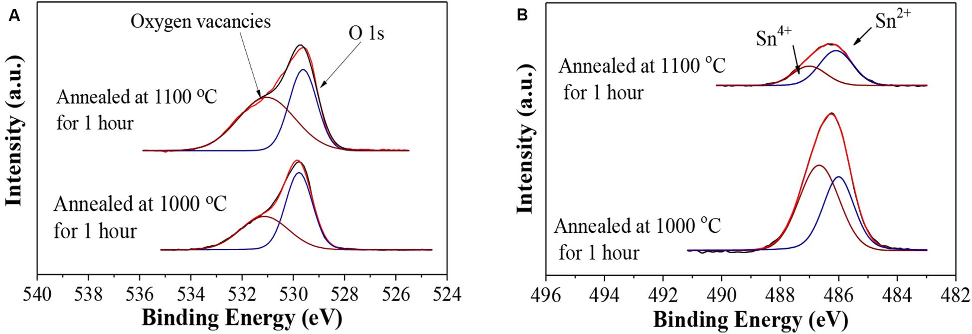
Figure 9. XPS spectra in the O1s (A), Sn4+ and Sn2+ (B) region for the ITO films annealed at 1,000°C for 1 h.
The main investigations into the high-temperature application of ITO films focuses on high temperatures below 800°C. The comparisons of results related to this study are shown in Table 3. This study has great advantages in terms of stable conductivity at high temperatures.
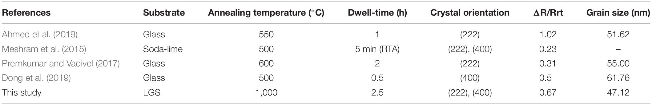
Table 3. Comparison of conductive ITO films at high temperatures.
Conclusion
In order to investigate the potential of conductive ITO films deposited by PLD on LGS substrates, a systematic set of annealing experiments was performed. The annealing temperature and dwell time were varied successively. The fact that the electrical characteristics of ITO films are sensitive to the microstructure and the chemical composition can be verified by the results as follows:
(1) For the ITO films, the changes in the conductivity during heating are mainly determined by two physical mechanisms: the distance between grain boundaries and the relative content of Sn4+ ions. During the process of heating, the increase in crystalline size decreases the distance between the grain boundaries. Additionally, the process of annealing in air reduces the number of oxygen vacancies, increasing the content of Sn4+ ions. Both of these behaviors are beneficial for decreasing the resistivity of the ITO films and enhancing the conductivity of the ITO films during the heating period (0–1,000°C).
(2) Indeed, the grain sizes hardly change during the whole heat preservation process at 1,000°C. In this case, the change in the conductivity is mainly determined by the chemical properties. The increase in oxygen defects and the decreased Sn4+ ion content have the opposite effect on the resistivity of ITO films heated at 1,000°C during the holding stage (1–4 h). The decisive factor for the sharply decreasing conductivity of the ITO films is the sharp reduction in the relative content of Sn4+ ions after 3 h at 1,000°C.
In general, the rules for the conductivity changes in ITO films annealed under different annealing process parameters have been investigated by the systematic analysis of the microstructure and the chemical composition of the Sn and O elements. The failure-mechanism for conductive ITO films was analyzed at extremely high-temperatures. It was found that a large amount of Sn4+ ion volatilization leads to a loss of conductivity. Moreover, the ITO films show a promising stability after 2.5 h at 1,000°C. The ITO films are a potential conductive material for special high-temperature applications up to 1,000°C, as they are expected to operate stably in high-temperature harsh environments.
Data Availability Statement
The original contributions presented in this study are included in the article/supplementary material, further inquiries can be directed to the corresponding author.
Author Contributions
HL and XL designed the experiments. XL performed the experiments. TS and QL analyzed the data. FZ and GX contributed the materials. XL and LG wrote the manuscript. TF and YC contributed to the modification and suggestion in this manuscript.
Funding
This study was supported by National Natural Science Foundation of China (Grant Nos. 11965009, 61874036, 61805053, and 61764001), Guangxi Innovation Research Team Project (Grant No. 2018GXNSFGA281004), Guangxi Science and Technology Planning Project (Grant Nos. AD18281030, AD18281084, AD18281034, AD18281037, and AD 19245066), Guangxi Natural Science Foundation (Grant Nos. 2016GXNSFDA380021, 2017GXNSFAA198164, 2018GXNSFBA050052, 2018GXNSFBA281152, and 2018GXNSFAA281201), Guangxi District Education Office projects to enhance the basic ability of young teachers, Innovation Project of GUET Graduate Education (Nos. 2018YJCXB15 and 2018YJCX25).
Conflict of Interest
The authors declare that the research was conducted in the absence of any commercial or financial relationships that could be construed as a potential conflict of interest.
References
Adurodija, F. O., Brüning, R., Asia, I. O., Izumi, H., Ishihara, T., and Yoshioka, H. (2005). Effects of laser irradiation energy density on the properties of pulsed laser deposited ITO thin films. Appl. Phys. A Mater. Sci. Process 81, 953–957. doi: 10.1007/s00339-005-3252-y
Adurodija, F. O., Izumi, H., Ishihara, T., Yoshioka, H., Yamada, K., Matsui, H., et al. (1999). Highly conducting indium tin oxide (ITO) thin films deposited by pulsed laser ablation. Thin. Solid Films 350, 79–84. doi: 10.1016/S0040-6090(99)00278-3
Ahmed, N. M., Sabah, F. A., Abdulgafour, H. I., Alsadig, A., Sulieman, A., and Alkhoaryef, M. (2019). The effect of post annealing temperature on grain size of indium-tin-oxide for optical and electrical properties improvement. Results Phys. 13:102159. doi: 10.1016/j.rinp.2019.102159
Brandes, E. A., and Brook, G. B. (1992). Smithells Metals Reference Book. Oxford: Butterworth Heinemann Press, 192–199.
Canhola, P., Martins, N., Raniero, L., Pereira, S., Fortunato, E., Ferreira, I., et al. (2005). Role of annealing environment on the performances of large area ITO films produced by rf magnetron sputtering. Thin. Solid Films 487, 271–276. doi: 10.1016/j.tsf.2005.01.078
Chung, C. H., Ko, Y. W., Kim, Y. H., Sohn, C. Y., Chu, H. Y., Park, S. H. K., et al. (2005). Radio frequency magnetron sputter-deposited indium tin oxide for use as a cathode in transparent organic light-emitting diode. Thin. Solid Films 491, 294–297. doi: 10.1016/j.tsf.2005.06.003
Diniz, A. S. A. C. (2011). The effects of various annealing regimes on the microstructure and physical properties of ITO (In2O3:Sn) thin films deposited by electron beam evaporation for solar energy applications. Renew. Energy 36, 1153–1165. doi: 10.1016/j.renene.2010.09.005
Dong, L., Zhu, G. S., Xu, H. R., Jiang, X. P., Zhang, X. Y., Zhao, Y. Y., et al. (2019). Preparation of indium tin oxide (ITO) thin film with (400) preferred orientation by sol–gel spin coating method. J. Mater. Sci. Mater. Electron. 30, 8047–8054. doi: 10.1007/s10854-019-01126-1
Granqvist, C. G., and Hultåker, A. (2002). Transparent and conducting ITO films: new developments and applications. Thin. Solid Films 411, 1–5. doi: 10.1016/S0040-6090(02)00163-3
Gregory, O. J., Luo, Q., and Crisman, E. E. (2002). High temperature stability of indium tin oxide thin films. Thin. Solid Films 406, 286–293. doi: 10.1016/S0040-6090(01)01773-4
Kanneboina, V., Madaka, R., and Agarwal, P. (2018). High open circuit voltage c-Si/a-Si:H heterojunction solar cells: influence of hydrogen plasma treatment studied by spectroscopic ellipsometry. Sol. Energy 166, 255–266. doi: 10.1016/j.solener.2018.03.068
Kato, K., Omoto, H., Tomioka, T., and Takamatsu, A. (2011). Optimum packing density and crystal structure of tin-doped indium oxide thin films for high-temperature annealing processes. Appl. Surf. Sci. 257, 9207–9212. doi: 10.1016/j.apsusc.2011.06.004
Ke, S., Chen, C., Fu, N., Zhou, H., Ye, M., Lin, P., et al. (2016). Transparent indium tin oxide electrodes on muscovite mica for high-temperature-processed flexible optoelectronic devices. ACS Appl. Mater. Interfaces 8, 28406–28411. doi: 10.1021/acsami.6b09166
Kim, H., Piqué, A., Horwitz, J. S., Mattoussi, H., Murata, H., Kafafi, Z. H., et al. (1999). Indium tin oxide thin films for organic light-emitting devices. Appl. Phys. Lett. 74, 3444–3446. doi: 10.1063/1.124122
Liu, J., and Zuo, Y. (2010). Crystallization and conductivity mechanism of ITO films on different substrates deposited with different substrate temperatures. J. Wuhan Univ. Technol. Mater. Sci. Ed. 25, 753–759. doi: 10.1007/s11595-010-0086-z
Liu, X., Peng, B., Zhang, W., Zhu, J., Liu, X., and Wei, M. (2017). Novel AlN/Pt/ZnO electrode for high temperature SAW sensors. Materials 10, 1–9. doi: 10.3390/ma10010069
Liu, X. P., and Peng, B. (2018). The improved Pt/ZnO/Al2O3 electrode for high temperature SAW sensors. IOP Conf. Ser. Earth Environ. Sci. 189, 1–6. doi: 10.1088/1755-1315/189/5/052032
Meshram, N., Loka, C., Park, K. R., and Lee, K. S. (2015). Enhanced transmittance of ITO/Ag(Cr)/ITO (IAI) multi-layered thin films by high temperature annealing. Mater. Lett. 145, 120–124. doi: 10.1016/j.matlet.2015.01.101
Nishio, K., Sei, T., and Tsuchiya, T. (1996). Preparation and electrical properties of ITO thin films by dip-coating process. J. Mater. Sci. 31, 1761–1766. doi: 10.1007/BF00372189
Park, Y. C., Kim, Y. S., Seo, H. K., Ansari, S. G., and Shin, H. S. (2002). ITO thin films deposited at different oxygen flow rates on Si(100) using the PEMOCVD method. Surf. Coatings Technol. 161, 62–69. doi: 10.1016/S0257-8972(02)00476-0
Premkumar, M., and Vadivel, S. (2017). Effect of annealing temperature on structural, optical and humidity sensing properties of indium tin oxide (ITO) thin films. J. Mater. Sci. Mater. Electron. 28, 8460–8466. doi: 10.1007/s10854-017-6566-6
Qin, K., Mei, F., Yuan, T., Li, R., Jiang, J., Niu, P., et al. (2018). Effects of sintering processes on the element chemical states of In, Sn and O in ITO targets. J. Mater. Sci. Mater. Electron. 29, 7931–7940. doi: 10.1007/s10854-018-8843-4
Reddy, I. N., Reddy, C. V., Cho, M., Shim, J., and Kim, D. (2017). Structural, optical and XPS study of thermal evaporated In2O3 thin films. Mater. Res. Express 4, 1–11. doi: 10.1088/2053-1591/aa7f59
Ren Xu, J., Yu Ming, Z., and Yi Men, Z. (2010). Calculation of dislocation destiny using X-Ray diffraction for 4H-SiC homoepitaxial layers. Guang Pu Xue Yu Guang Pu Fen Xi 30, 1995–1997. doi: 10.3964/j.issn.1000-059307-1995-03
Sawada, M., Higuchi, M., Kondo, S., and Saka, H. (2001). Characteristics of indium-tin-oxide/silver/indium-tin-oxide sandwich films and their application to simple-matrix liquid-crystal displays. Jpn. J. Appl. Phys. I Regul. Pap. Short Notes Rev. Pap. 40, 3332–3336. doi: 10.1143/jjap.40.3332
Song, S., Yang, T., Liu, J., Xin, Y., Li, Y., and Han, S. (2011). Rapid thermal annealing of ITO films. Appl. Surf. Sci. 257, 7061–7064. doi: 10.1016/j.apsusc.2011.03.009
Sun, K., Zhou, W., Tang, X., and Luo, F. (2016). Application of indium tin oxide (ITO) thin film as a low emissivity film on Ni-based alloy at high temperature. Infrared Phys. Technol. 78, 156–161. doi: 10.1016/j.infrared.2016.07.021
Toušková, J., Kovanda, J., Dobiášová, L., Paøízek, V., and Kielar, P. (1995). Sputtered indium-tin oxide substrates for CdS-CdTe solar cells. Sol. Energy Mater. Sol. Cells 37, 357–365. doi: 10.1016/0927-0248(95)00029-1
Yang, B. Y., Huang, Q., Metz, A. W., Ni, J., Jin, S., Marks, T. J., et al. (2004). High-performance organic light-emitting diodes using ITO anodes grown on plastic by deposition. Adv. Mater. 4, 321–324. doi: 10.1002/adma.200305727
Zhang, Y., Cheng, P., Yu, K., Zhao, X., and Ding, G. (2017). ITO film prepared by ion beam sputtering and its application in high-temperature thermocouple. Vacuum 146, 31–34. doi: 10.1016/j.vacuum.2017.08.046
Keywords: ITO, extremely high temperature, conductivity, microstructural, chemical properties
Citation: Li H, Guo L, Liu X, Sun T, Li Q, Zhang F, Xiao G, Fu T and Chen Y (2020) High Temperature Conductive Stability of Indium Tin Oxide Films. Front. Mater. 7:113. doi: 10.3389/fmats.2020.00113
Received: 05 February 2020; Accepted: 14 April 2020;
Published: 22 May 2020.
Edited by:
Bernardo Mendoza, Centro de Investigaciones en Optica, MexicoReviewed by:
Manuel Pereira Dos Santos, University of Evora, PortugalIbrahim Sayed Hussein, King Khalid University, Saudi Arabia
Copyright © 2020 Li, Guo, Liu, Sun, Li, Zhang, Xiao, Fu and Chen. This is an open-access article distributed under the terms of the Creative Commons Attribution License (CC BY). The use, distribution or reproduction in other forums is permitted, provided the original author(s) and the copyright owner(s) are credited and that the original publication in this journal is cited, in accordance with accepted academic practice. No use, distribution or reproduction is permitted which does not comply with these terms.
*Correspondence: Xingpeng Liu, tadyliu@guet.edu.cn; Tangyou Sun, suntangyou@guet.edu.cn