

Abstract
We have addressed density of states and electrical conductivity of doped graphene like nanotubes for both zigzag and armchair types in the context of tight binding model hamiltonian. The effects of next nearest neighbor hopping amplitude for electrons and gap parameter on electronic density of states and electrical conductivity have been investigated. Green's function approach has been implemented to find the behavior of electrical conductivity of nanotube within linear response theory. We have found the temperature dependence of electrical conductivity for different values of gap parameter and tube diameter in the presence of neat nearest neighbor hopping integral. The results of electrical conductivity show the increase of diameter leads to increase the conductivity of both zigzag and armchair nanotubes. However the increase of chemical potential reduces the conductivity of armchair nanotube. In the presence of next-to-nearest neighbor hopping amplitude, the density of states results of nanotubes loses its symmetry with respect to energy.
Export citation and abstract BibTeX RIS
The physics of one-dimensional systems has been a rich and active playground for theorists for mere than 50 years, with major conceptual breakthroughs arising from the specific properties of the confined electron gas. The difficulty in synthesizing clean one dimensional systems with metallic behavior has for many decades confined this theoretical work to formal developments and unverified predictions.1,2 The technological interest in controlling the properties of nanosized and plastic conductors was a strong driver for exploring this field.
The field of nanotubes has strongly benefited from this broad fundamental and technological interest. These nanoscale graphitic structure are of great interest for both theoretical and experimental solid state physicists in during the past two decades.1 These materials1,2 are formed from carbon atoms arranged on rolled honeycomb lattice as cylindrical structure with nanometer diameter and micrometer length. Nanotubes are considered as either single molecules or quasi one dimensional crystals with translational periodicity along the tube axis. A single wall carbon nanotube(SWCNT) is predicted to be either a metal or a semiconductor, depending on its radius and chirality.2 Nanotubes are also mechanically very stable and strong, and their carrier mobility is equivalent to that of good metals, suggesting that they would make ideal interconnects with remarkable transport properties in nanosized devices.3,4 One of the significant transport properties of CNTs has been the high values of electrical conduction of CNTs that leads to attract considerable attention.5
In practice, metallic carbon nanotubes are very good conductors exhibiting ballistic transport properties.6 Simple circuits based on semiconducting carbon nanotube field effect transistors have already been demonstrated.7 Mobility of electrons can be as high as 79 000 cm2 V−1 s at room temperature for semiconducting CNT field effect transistor with channel lengths of more than 300 μm.8 Therefore the understanding the mechanisms of reduction of electron mobility due to various scattering effects by simulating the nanotubes can be considered as a novel topic. The effects of impurities produced in the CNT on transport properties or mobility of electrons have already been investigated theoretically.9 Measurements of the magneto conductance of a single multi-shell nanotube in a two probe configuration showed that the transport is characterized by disorder and localization phenomena.10 The conductivity spectra in far infrared range have shown to exhibit a broad band structure with its peak located around 10–30 meV, which has been attributed to the curvature-induced small gaps,11 or plasmon resonance. The behavior of thermal conductivity of CNT in the presence of lattice vibrations has been investigated in an experimental work.12 It is should be noticed some aspects of electronic properties of nanotubes such as charge density wave and superconductivity instabilities can be understood due to consider coupling of electrons with optical phonons.13,14 Boltzmann approach is not valid to treat optical phonons due to their high energy that leads to appear interband transition at typical density. Under this circumstance, Kubo formula15 is applied to find transport properties such as electrical conductivity. Static transport in few-layer graphene have been studied for both without and in the presence of a magnetic field. It is established that charged impurity scattering is primarily responsible for the transport behavior observed in monolayer graphene.16 A comprehensive study of the electronic properties of the graphene in the presence of defects as a function of temperature, external frequency, gate voltage, and magnetic field has been presented by Peres and coworkers.17
Most electronic applications of nanotubes are based on the presence of a gap between the valence and conduction bands in the conventional semiconductors. The bandgap is a measure of the threshold voltage and on-off ratio of the field effect transistors.18,19 Therefore for integrating graphene like structures into semiconductor technology, it is crucial to induce a bandgap in band structure of graphene like structures to control the transport of carriers. Several routes have being proposed and applied to induce and control a gap in graphene. One of them is using quantum confined geometries such as quantum dots and nanoribbons.20,21 Another way is spin-orbit coupling whose origin is due to both intrinsic spin-orbit interactions and Rashba interaction.22,23 Also inversion symmetry breaking of the sublattices gives rise to a gap in the single-particle excitation spectrum24 which introduces the gap parameter Δ as an energy scale. The gapped graphene can be modeled with 2+1 dimensional massive Dirac fermions. This parameter leads to a charge gap of magnitude 2Δ in the spectrum of single-particle excitations and a trivial band insulator is developed.25
In this paper, we address the effects of next nearest neighbor hopping of electrons, tube diameter and energy gap on the static electrical conductivity of doped graphene like nanotubes in the context of tight binding approximation. The electrical properties of both zigzag and armchair folding types have been investigated due to the effects of next nearest neighbor hopping amplitude. Also the energy dependence of total density of states in the presence of the effects of next nearest neighbor hopping, gap parameter and tube diameter has been studied for both nanotube types. Linear response theory has been implemented to derive static electrical conductivity alone tube axis. We have exploited Green's function approach to calculate the electrical conductivity, i.e. the time ordered electrical current correlation. The effects of energy gap, chemical potential and folding types on the temperature dependence of electrical conductivity of graphene like nanotubes have been studied. Also we study the dependence of static electrical conductivity of nanotubes on chemical potential for both types of tube folding. Also we have addressed the behavior of electrical conductivity in terms of chemical potential for different diameters and gap parameter in details.
Model and Method
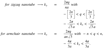
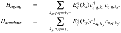
In this work, we apply tight binding model Hamiltonian to describe electrons on the honeycomb lattice. To calculate the electrical conductivity of graphene like nanotube we consider monolayer graphene which is folded along zigzag or armchair directions. The lattice structure of each graphene layer has been shown in Fig. 1. The primitive unit cell vectors are given by
where  and
and  are unit cell vectors along zigzag and armchair directions, respectively. Also the length of unit cell vectors is considered to be a. In order to obtain electrical transport properties of graphene like nanotubes we must first examine the band structure and provide the expression for the electronic Green's function. We start from a tight binding model incorporating nearest and next nearest neighboring hopping terms. A finite difference between on-site energies of two different sublattice atoms of honeycomb structure has been applied in the model Hamiltonian. Up to the next nearest neighbor approximation, the spin independent tight binding model hamiltonian for monolayer graphene (H) is given by
In Eq. 2,  denotes the annihilation operator for an electron which is on an A(B)-atom site with unit cell label i in the graphene layer.
  in Eq. 2 indicates the on-site energy of electrons on atoms of sublattice A. Also Δ introduces the gap parameter.
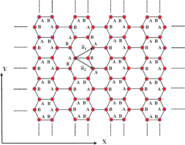
Figure 1. Crystal structure of honeycomb lattice with two different sublattices.  and
and  are the primitive unit cell vectors.
Download figure:
Standard image High-resolution imageδ is one of three vectors that connects the unit cells of nearest-neighbor lattice sites and given by  according to Fig. 1. Moreover
  connects the unit cells of next nearest-neighbor lattice sites and is one of the six vectors given by
  .
.
 is the nearest neighbour intralayer hopping terms for electrons to move within a given plane.
  refers to the next nearest neighbor hopping integral for electrons. μ introduces the chemical potential which determines the electron density. The following Fourier transformations for fermionic operators
  ,
,  have been given by

where N is the number of unit cells and  introduces the position vector of i th unit cell in graphene layer.
  is wave vector belonging to the first Brillouin zone of nanotube structure. Depending on the zigzag or armchair type of nanotube, the region of wave vectors
  are determined. Based on Fig. 1, axis direction of zigzag nanotube is resulted to be along x. In other words nanotubes of the type
  are called zigzag tubes, because they exhibit a zigzag pattern along the circumference. A single-wall zigzag nanotube is geometrically obtained by rolling up a single graphene layer around x direction according to Fig. 1. We introduce
  is the length of circumference of zigzag nanotube. a denotes the length of each of unit cell vector. Periodic boundary condition for zigzag nanotube
  define the small number of allowed wave vectors ky in the circumferential direction

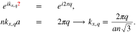
where integer quantum number q is determined using the first Brillouin zone of honeycomb structure. Based on the first Brillouin zone of honeycomb lattice ky is into the region  . Using Eq. 4, one can write
  . Thus we have
 ![$-\left[\tfrac{2n}{3}\right]\lt q\lt \left[\tfrac{2n}{3}\right]$](https://content.cld.iop.org/journals/2162-8777/9/5/051002/revision2/jssab92acieqn22.gif) for zigzag nanotube
for zigzag nanotube  . A similar way can be considered for finding the region of wave vectors of armchair graphene like nanotube. Nanotubes of the type
  are called zigzag tubes, because they exhibit an armchair pattern along the circumference. A single-wall armchair nanotube is geometrically obtained by rolling up a single graphene layer around y direction according to Fig. 1. The length of circumference of zigzag nanotube is obtained as
  . Now periodic boundary condition for zigzag nanotube
  define the small number of allowed wave vectors ky in the circumferential direction
The integer quantum number q is determined using the first Brillouin zone of honeycomb structure. Based on Fig. 1 and the first Brillouin zone of honeycomb structure, kx satisfies the expression  . Using Eq. 4, one can write
 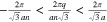 . Thus we have
  for armchair nanotube
  . Based on above statements, we can introduce the following wave vector regions for each type of nanotube
In terms of Fourier transformation of operators, one can rewrite the clean tight binding part of the Hamiltonian in Eq. 2 as
in which the vector of fermion creation operators is defined as  . Under next-to-nearest neighbor approximation the following matrix form for
  is given as

Using the definitions for δ and  the functions
  and
and  are expressed based on the following relations

where the components of wave vector  for each zigzag or armchair nanotube obey the relations in Eq. 6. After diagonalizing of the Hamiltonian in Eq. 8, the band structures of single wall graphene like zigzag nanotube
  are given by following eigenvalues
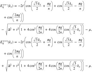
Also the band structure of single wall graphene like armchair nanotube  in the presence of next nearest neighbor hopping and gap parameter is readily obtained as following expression

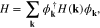
Using band energy spectrum in Eq. 10, the Hamiltonian in Eq. 7 for zigzag and armchair nanotubes can be rewritten by
The electronic Green's functions of each nanotube can be defined using the Hamiltonian in Eq. 12 as following expression

where τ is imaginary time. Using the model Hamiltonian in Eq. 12, the Fourier transformations of Green's function of each nanotube is given by
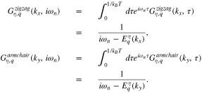
Here  denotes the fermionic Matsubara frequency in which T is equilibrium temperature. In the following, the expression of electrical electrical conductivity of graphene like nanotube are presented using Green's function method.15 Based on linear response theory,15 Kubo formulas gives us the dynamical electrical conductivity (
 ) along axis direction of nanotube (ζ) in terms of correlation function between electrical currents15 as
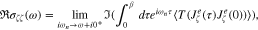
where  introduces the operator from of electrical current along nanotube axis direction. We have studied the conductivity of zigzag nanotube along its axis, i.e. x direction. Also the conductivity of armchair nanotube is calculated along y direction.
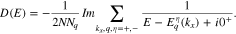
  denotes the bosonic Matsubara frequency. The static transport coefficients for single band model Hamiltonian26 have been obtained in terms of Green's function. One can generalize this result for multiband model Hamiltonian and the static electrical conductivity of graphene like zigzag nanotube
  along
along  direction is related Green's function as

where  is the Fermi-Dirac distribution function and T denotes the equilibrium temperature. N is the number of kx points and Nq implies the number of integer quantum number q. The static electrical conductivity of graphene like armchair nanotube
  along
along  direction, i.e. axis direction of tube, is written in terms of Green's function as

Substituting electronic Green's function into Eqs. 16, 17 and performing the numerical integration over wave vector through first Brillouin zone, the results of electrical conductivity have been obtained. The electronic density of states of graphene like zigzag and armchair nanotubes in the presence of gap parameter and next nearest neighbor hopping integral can be obtained by electronic band structure as
Also we have the following expression for electronic density of states of armchair nanotube
The study of temperature behavior of electrical conductivity along nanotube axis for both zigzag and armchair graphene nanotubes in the presence of naex-to-nearest neighbor hopping amplitude constitutes is the main aim in this work. Moreover the energy dependence of electronic density of states of nanotubes is investigated in details.
Numerical Results and Discussion
We turn to the presentation of our numerical results of the static electrical conductivity of both armchair and graphene like nanotubes due to effects of next nearest neighbor hopping of electrons and tube diameter. The electrical conductivity of doped zigzag and armchair nanotubes in the presence of gap parameter has been obtained using tight binding model Hamiltonian. The temperature behavior of electrical conductivity has been found via calculating the current-current correlation function within Green's function approach. Also the effects of gap parameter, next nearest neighbor hopping amplitude and diameter on the behavior of density of states of nanotubes have been addressed. By evaluating Eqs. 16, 17 numerically and using Green's functions in Eq. 14, electrical conductivity of both zigzag and armchair nanotubes has been found. In order to perform the summation over  points, we can exploit the wave vector region for zigzag and armchair nanotubes presented in Eq. 6. The contribution of both inter and intra band transitions to the static electrical conductivity has been accounted. The numerical results of conductivity have been presented by considering next nearest neighbor hopping amplitude as
  .
.
The total density of states ( ) of zigzag nanotube as a function of normalized energy E/t in the absence of gap parameter
  for different values of tube diameter
  has been shown in Fig. 2. The effect of next nearest neighbor hopping integral shows that density of states curves has no symmetry around Fermi level at
  according to Fig. 2. This arises from this fact that electron-hole symmetry breaks when the next-to-nearest neighbor hopping amplitude
  is taken into account. Figure 2 shows the density of states at Fermi level gets the non zero value for each diameter. Thus undoped zigzag nanotubes with different diameters indicate metallic behavior in the presence of next nearest neighbor hopping amplitude. A sharp peak with high intensity is observed for zigzag nanotube
  in conduction band side around
  . Such sharp peak in density of states is an evidence for stable quantum energy level for infinite life time. However all zigzag nanotubes show considerable sharp peaks in valence band around
  . In the absence of next nearest neighbor hopping, the density of states curves present an even function in terms of energy E. In other words the behavior of density of states in terms of energy is fully symmetric around
  . While the density of states loses such symmetry in the presence of next nearest neighbor hopping.
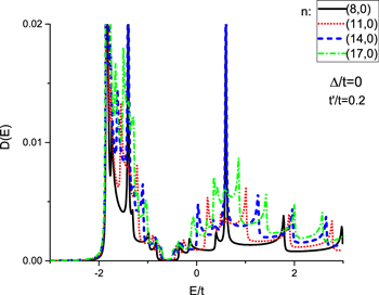
Figure 2. Electronic density of states of undoped graphene like zigzag nanotube for different values of tube diameter in the presence of next nearest neighbor hopping amplitude  . The Fermi level is located at
  in this figure. n characterizes the index of tube so that the tube diameter is related to n.
Download figure:
Standard image High-resolution imageThe effect of gap parameter on energy dependence of density of states of undoped graphene like zigzag nanotube  in the presence of next-to-nearest neighbor hopping amplitude has been plotted in Fig. 3. The gap parameters below 0.4 preserve the metallic property of zigzag nantube so that the density of states at Fermi energy gets the non zero value. For gap parameters above 0.4, namely
  , the Fermi energy locates in bandgap and an insulator phase develops as shown in Fig. 3. Moreover the considerable sharp peaks with high intensity are clearly observed for all values of gap parameters. According to Fig. 3, density of states is no longer even with respect to energy due to the next nearest neighbor hopping amplitude.
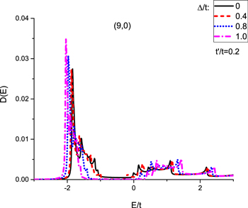
Figure 3. Electronic density of states of undoped graphene like zigzag nanotube (9, 0) for different gap parameters, namely  in the presence of next nearest neighbor hopping amplitude
  . The Fermi level is located at
  in this figure.
Download figure:
Standard image High-resolution imageThe density of states ( ) of armchair nanotube as a function of normalized energy E/t in the absence of gap parameter
  for different values of tube diameter
  has been shown in Fig. 4. Density of states curves show a metallic behavior for all tube diameter since the density of states takes a non zero value at Fermi energy. This metallic property is improved with diameter. Moreover a considerable sharp peak with high intensity is observed at
  for each diameter according to Fig. 4.
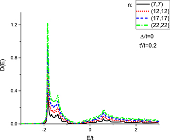
Figure 4. Electronic density of states of undoped graphene like armchair nanotube for different values of tube diameter in the presence of next nearest neighbor hopping amplitude  . n characterizes the index of tube so that the tube diameter is related to n.
Download figure:
Standard image High-resolution imageThe behavior of density of states of undoped graphene like armchair nanotube  for different gap parameters Δ in the presence of next-to-nearest neighbor hopping amplitude
  has been shown in Fig. 5. The value of density of states at Fermi energy for
  is non zero and thus metallic property is preserved at these gap parameters. Upon more increasing gap parameters, namely
  , the Fermi energy locates into bandgap and we observe an insulating behavior for
  . The considerable peaks in density of states moves to lower energy however the height of peaks increases with Δ as shown in Fig. 5.
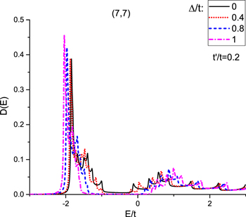
Figure 5. Electronic density of states of undoped graphene like armchair nanotube (7, 7) for different values of gap parameters, namely  in the presence of next nearest neighbor hopping amplitude
  .
.
Download figure:
Standard image High-resolution imageWe have studied temperature behavior of electrical conductivity of armchair nanotube along tube axis. In Fig. 6, we have depicted temperature dependence of electrical conductivity, σ, along nanotube axis of the undoped graphene like zigzag nanotube for different values of diameters, namely  by setting
  . Gap parameter Δ has been considered to be zero. For each value of tube diameter n, this figure shows electrical conductivity increases with temperature up to a characteristic temperature where conductivity reaches its maximum value. Temperature position of peak is approximately independent of tube diameter according Fig. 6. For temperatures below peak position, electronic transition rate from valence band to conduction one increases and consequently we observe an increasing behavior for conductivity in this temperature region. Upon more increasing temperature above peak position, a decreasing behavior for electrical conductivity has been observed due to increase of electronic scattering in this temperature region. The origin of the peak arises from the competition between electronic transition rate from valence band to conduction one and scattering rate between electrons. At a fixed temperature, electrical conductivity increases with tube diameter n. In fact the metallic property of armchair nanotube in the presence of next-to-nearest neighbor hopping is improved with diameter.
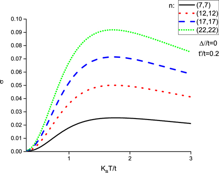
Figure 6. Static electrical conductivity (σ) of armchair graphene nanotube as a function of normalized temperature ( ) for various tube diameter n at zero gap parameter in the presence of next-to-nearest neighbor hopping.
Download figure:
Standard image High-resolution imageThe effect of gap parameter  on temperature dependence of electrical conductivity of undoped graphene like armchair nanotube has been studied in Fig. 7. An exponential behavior for electrical conductivity is clearly observed at low temperatures for finite value of gap parameter. There is a peak in electrical conductivity for each value of gap parameter. For temperatures below peak position, the increase of temperature leads to enhance the electronic transition from valence band to conduction one. Thus conductivity rises with temperature up to temperature position of peak. Upon more increasing temperature above peak position, the conductivity reduces with temperature due to increase of scattering rate between electrons. In addition, at fixed values of temperatures, lower gap parameter gives arise more transition rate of electrons and consequently higher values in electrical conductivity according to Fig. 7.
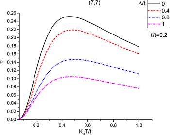
Figure 7. Static electrical conductivity (σ) of armchair graphene nanotube  as a function of normalized temperature (
 ) for various gap parameters
  in the presence of next-to-nearest neighbor hopping.
Download figure:
Standard image High-resolution imageWe have also studied the effect of electron density, i.e. the variation of chemical potential μ, on electrical conductivity of doped armchair nanotube in the presence of next nearest neighbor hopping amplitude. The resulting of the electrical conductivity of armchair nanotube as a function of normalized chemical potential  for different tube diameters n is summarized in Fig. 8. Gap parameter has been considered to be zero. Figure 8 shows the electrical conductivity reduces with chemical potential for all tube diameters. However the conductivity is less chemical potential dependent at normalized temperatures below 1.0 for
  as shown in Fig. 8. Moreover the electrical conductivity rises with tube diameter at fixed values of chemical potential.

Figure 8. Static electrical conductivity (σ) of armchair graphene nanotube as a function of normalized chemical potential ( ) for various tube diameter n in the presence of next-to-nearest neighbor hopping.
Download figure:
Standard image High-resolution imageThe dependence of electrical conductivity of zigzag nanotube on chemical potential has been presented in Fig. 9. In this figure we have plotted the electrical conductivity of zigzag nanotubes as a function of normalized chemical potential  for different values of n. Two novel features are pronounced in Fig. 9. In contrast to Fig. 8, there is no considerable diameter dependence for electrical conductivity. Furthermore, the conductivity reaches its maximum value at normalized chemical potential 0.25 for all values of diameter n. Also the conductivity vanishes for chemical potentials above 0.9.
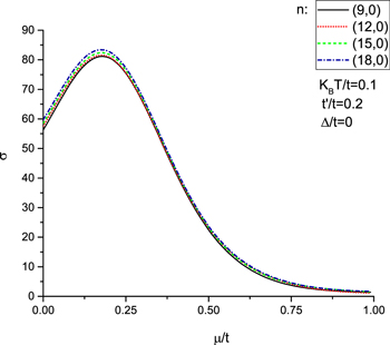
Figure 9. Static electrical conductivity (σ) of zigzag graphene nanotube as a function of normalized chemical potential ( ) for various tube diameters n at zero gap parameter
  in the presence of next-to-nearest neighbor hopping.
Download figure:
Standard image High-resolution imageThe numerical results of electrical conductivity of zigzag nanotube  for different gap parameters, namely
  , for normalized temperature
  have been shown in Fig. 10. A monotonic increasing behavior for dependence of electrical conductivity on chemical potential has been observed for
  . The dependence of conductivity on chemical potential for
  is not remarkable. In addition, at fixed temperature, the conductivity decreases with gap parameter Δ according to Fig. 10. It can be understood from this fact that the increase of gap parameter leads to reduce the transition rate of electrons an thus electrical conductivity decreases with Δ.
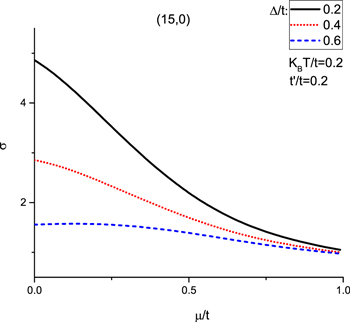
Figure 10. Static electrical conductivity (σ) of zigzag graphene nanotube  as a function of normalized chemical potential (
 ) for various gap parameters Δ in the presence of next-to-nearest neighbor hopping. Temperature has been fixed at
  .
.
Download figure:
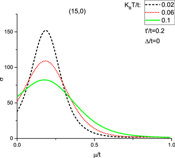
Standard image High-resolution imageFinally we have plotted the electrical conductivity of zigzag nanotube as a function of normalized chemical potential for different values of temperature  for
for  in the absence of gap parameter. This figure implies the conductivity reduces with temperature in the chemical potentials region
  . A peak is clearly observed at chemical potential around
  for each value of temperature. For fixed chemical potential above 0.4, the conductivity increases with temperature according to Fig. 11. The conductivity goes to zero at chemical potentials above 0.75 for all temperatures due to increase of scattering rate between electrons in this region.
Figure 11. Static electrical conductivity (σ) of zigzag graphene nanotube  as a function of normalized chemical potential (
 ) for various normalized temperatures
  at zero gap parameter in the presence of next-to-nearest neighbor hopping.
Download figure:
Standard image High-resolution image
Conclusions
In conclusion, we have presented the temperature dependence of electrical conductivity of graphene like nanotubes in the presence of electron doping which means the increasing the concentration of electrons in the system via adding impurity atoms to the structure. Using a tight binding model Hamiltonian and a Green's function approach the excitation spectrum of the model Hamiltonian has been studied. In particular, the effect of gap parameter on electrical conductivity and density of states has been investigated. The increase of gap parameter leads to decrease of electrical conductivity. Moreover at a fixed temperature, the increase of tube diameter of armchair nanotube causes to the enhancement of electrical conductivity. In other hand our results show that an increase of the chemical potential gives rise to an increas of electrical conductivity.