Review

Unseeded Crystal Growth of (100)-Oriented Grain-Boundary-Free Si Thin-Film by a Single Scan of the CW-Laser Lateral Crystallization of a-Si on Insulator

1
Sasaki Consulting, Kawasaki 212-0012, Japan
2
Division of Materials Science, NAIST, Ikoma 630-0192, Japan
3
V-Technology, Yokohama 240-0005, Japan
*
Author to whom correspondence should be addressed.
Crystals 2020, 10(5), 405; https://doi.org/10.3390/cryst10050405
Submission received: 14 April 2020 / Revised: 3 May 2020 / Accepted: 12 May 2020 / Published: 17 May 2020
(This article belongs to the Special Issue Growth and Evaluation of Crystalline Silicon (Volume II))

Abstract

:
Laser crystallization of a-Si film on insulating substrate is a promising technology to fabricate three-dimensional integrations (3D ICs), flat panel displays (FPDs), or flexible electronics, because the crystallization can be performed on room temperature substrate to avoid damage to the underlying devices or supporting plane. Orientation-controlled grain-boundary-free films are required to improve the uniformity in electrical characteristics of field-effect-transistors (FETs)fabricated in those films. This paper describes the recently found simple method to obtain {100}-oriented grain-boundary-free Si thin-films stably, by using a single scan of continuous-wave (CW)-laser lateral crystallization of a-Si with a highly top-flat line beam with 532 nm wavelength at room temperature in air. It was difficult to control crystal orientations in the grain-boundary-free film crystallized by the artificial modulation of solid-liquid interface, and any other trial to obtain preferential surface orientation with multiple irradiations resulted in grain boundaries. The self-organized growth of the {100}-oriented grain-boundary-free films were realized by satisfying the following conditions: (1) highly uniform top-flat line beam, (2) SiO2 cap, (3) low laser power density in the vicinity of the lateral growth threshold, and (4) single scan crystallization. Higher scan velocity makes the process window wide for the {100}-oriented grain-boundary-free film. This crystallization is very simple, because it is performed by a single unseeded scan with a line beam at room temperature substrate in air.

1. Introduction

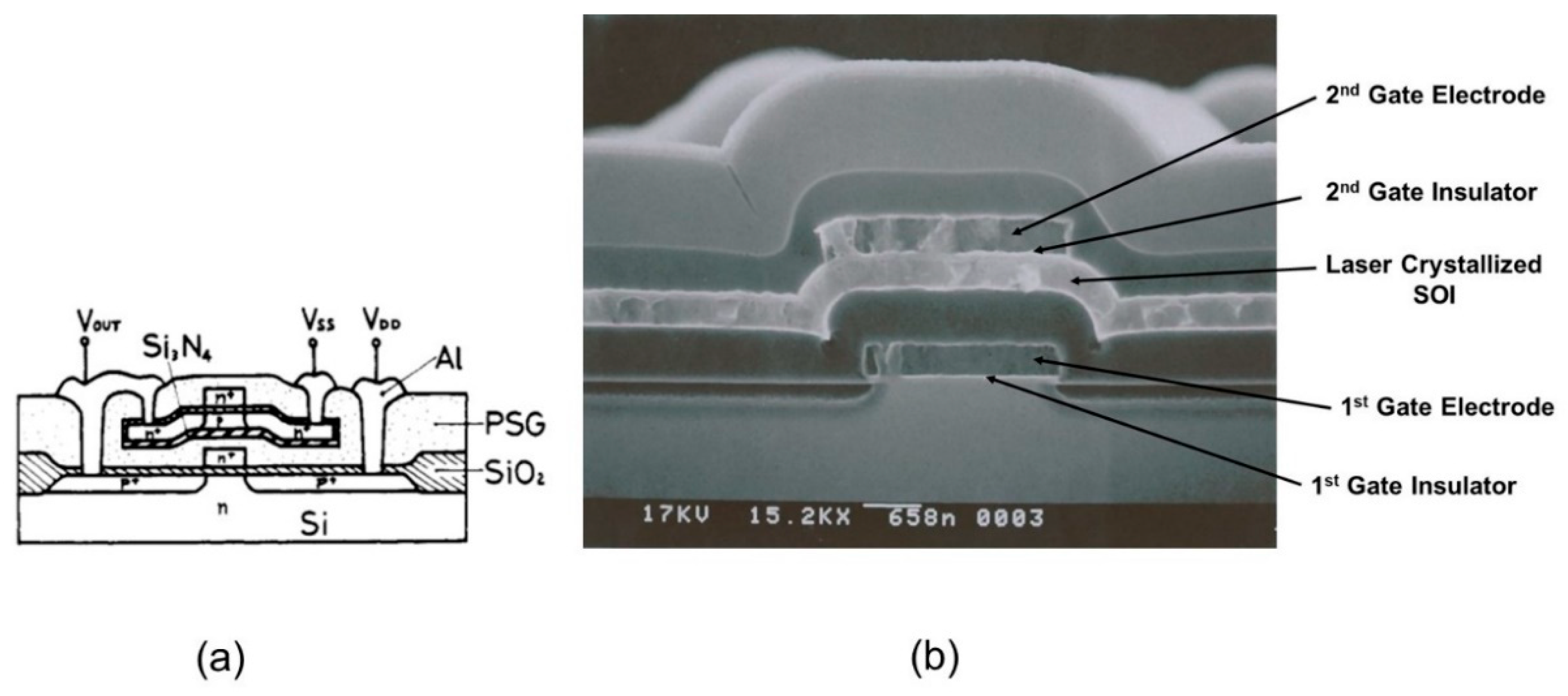
1.1. Necessity for Laser Crystallization

Demand for monolithic three-dimensional integrations (3D ICs) [1,2], flat panel displays (FPDs) on flexible substrates, or flexible electronics have been increased recently. To make those devices, it is necessary to realize high performance and high uniformity of the silicon-on-insulator (SOI)field-effect-transistors (FETs)or thin-film transistors (TFTs) in stacked Si thin-film structures, keeping the substrate at low temperature. The performance and reliability of Si devices is much superior to those of oxide [3] or organic devices [4]. Laser crystallization of a-Si on insulating substrate can grow crystalline Si thin-films, avoiding the substrate temperature rise by utilizing the appropriate buffer layers. The buffer layers are used to thermally isolate the surface molten pool from the underlying low temperature substrate. Figure 1 shows a cross-sectional SEM image of the first ever fabricated monolithic stacked 3D IC: a seven-stage CMOS ring oscillator [5]. N- and p-MOS transistors are stacked on each other, making a 3D CMOS inverter as a circuit element. The n-MOS SOI-FETs in the film crystallized by the continuous-wave (CW) laser were fabricated just above the bulk p-MOS FETs, but these SOI films contained grain boundaries and showed random crystalline orientations.
Orientation-controlled and grain-boundary-free films are necessary to realize high performance and high uniformity of the electrical characteristics of SOI-FETs or TFTs, because crystalline defects, such as grain boundaries, affect threshold voltage [6] and field effect mobility [7], and crystal orientation again affects threshold voltage [8] and field effect mobility [9,10]. Previously, the grain-boundary-free {100} surface textured Si films of 50 nm–5 μm thickness on insulators were fabricated by using a strip-heater zone-melt recrystallization (ZMR) as well [11,12,13,14,15,16,17,18], but ZMR cannot be applied to the present day thin-film applications, because of the necessity of the substrate to be pre-heated to 1100–1300 °C in ZMR [11]. The crystallization must be carried out for Si thin-film at the substrate temperature of less than 400–500 °C to make monolithic 3D ICs, FPDs, or flexible electronics to avoid damage to the underlying layer.

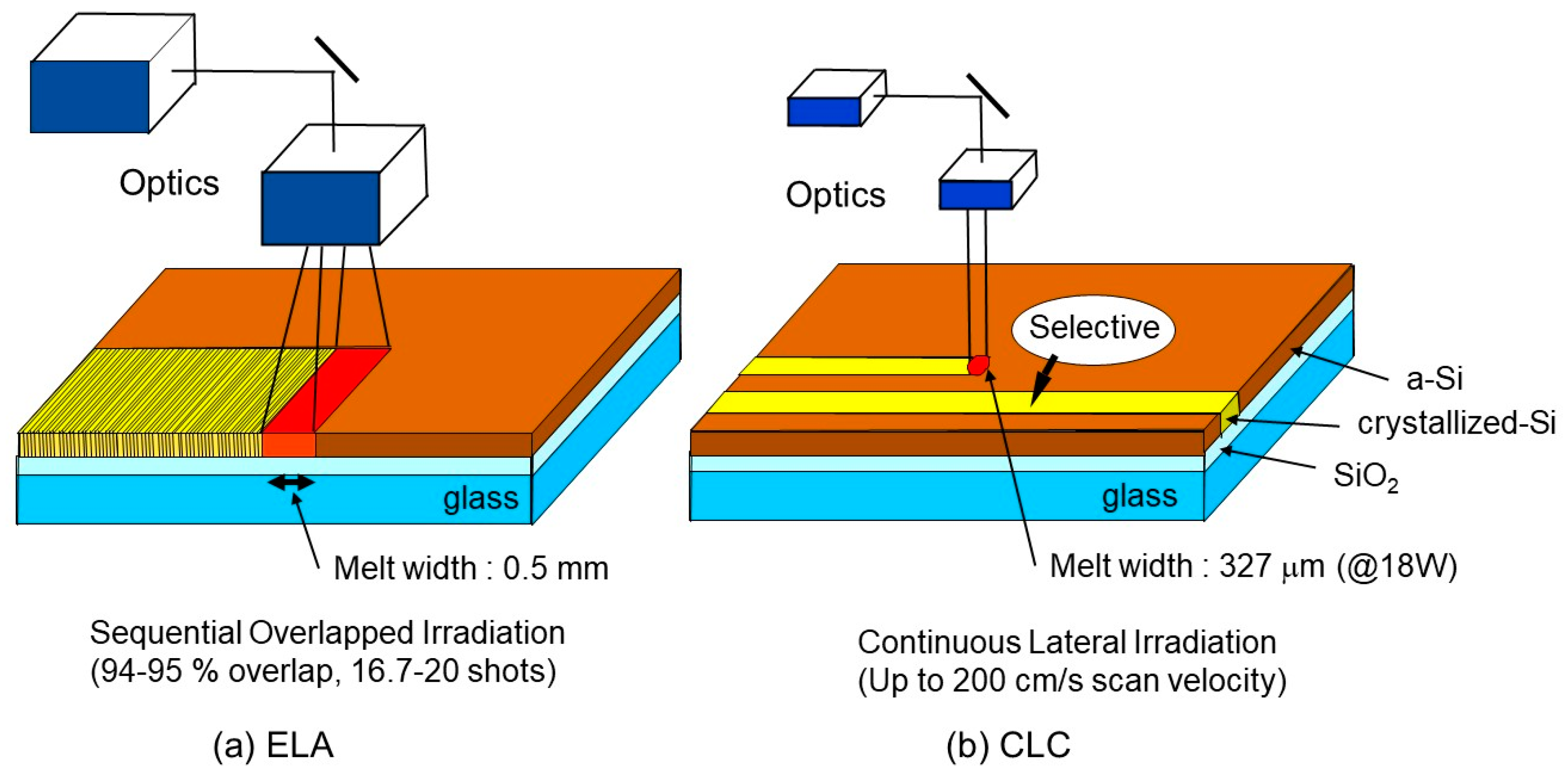
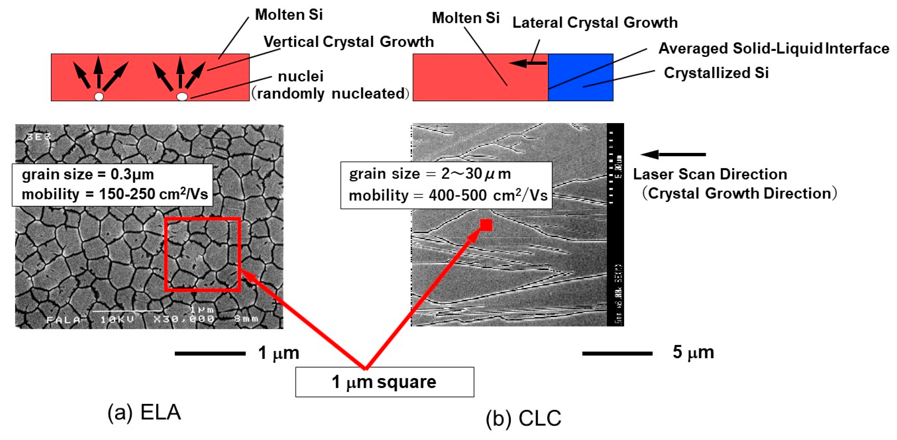
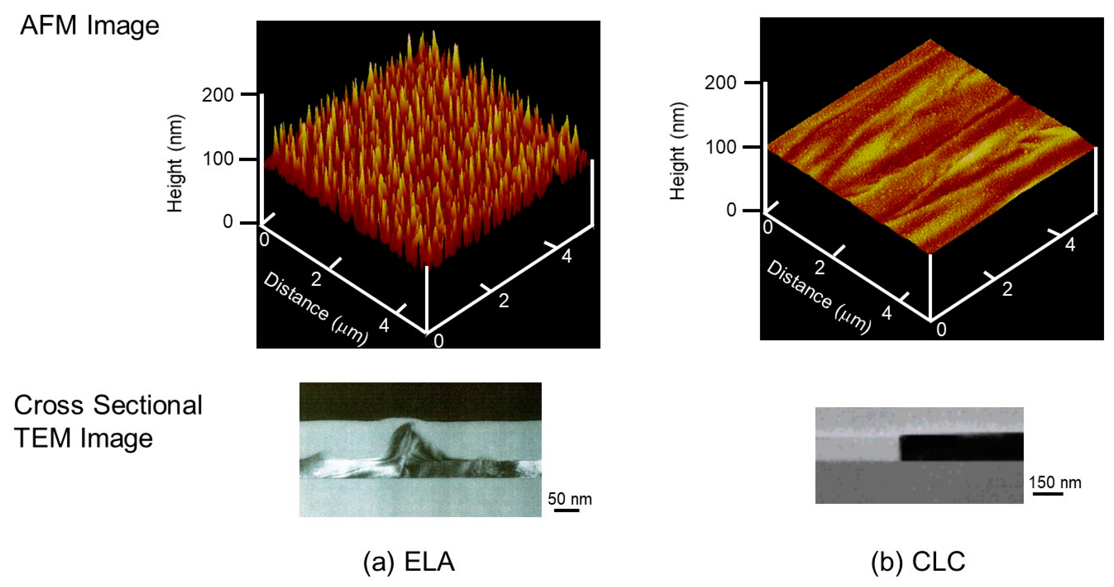
1.2. Comparison Between Continuous-Wave (CW)-Laser Lateral Crystallization (CLC) and Pulse Excimer Laser Annealing (ELA)
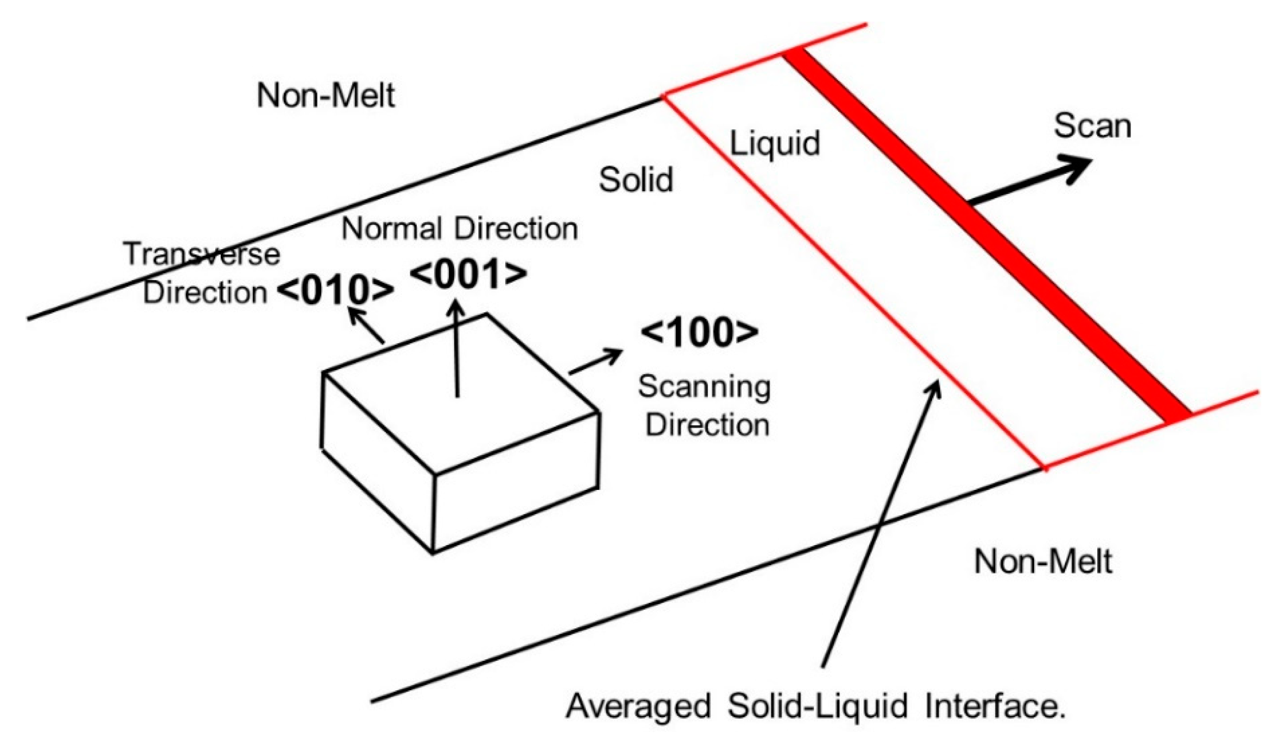
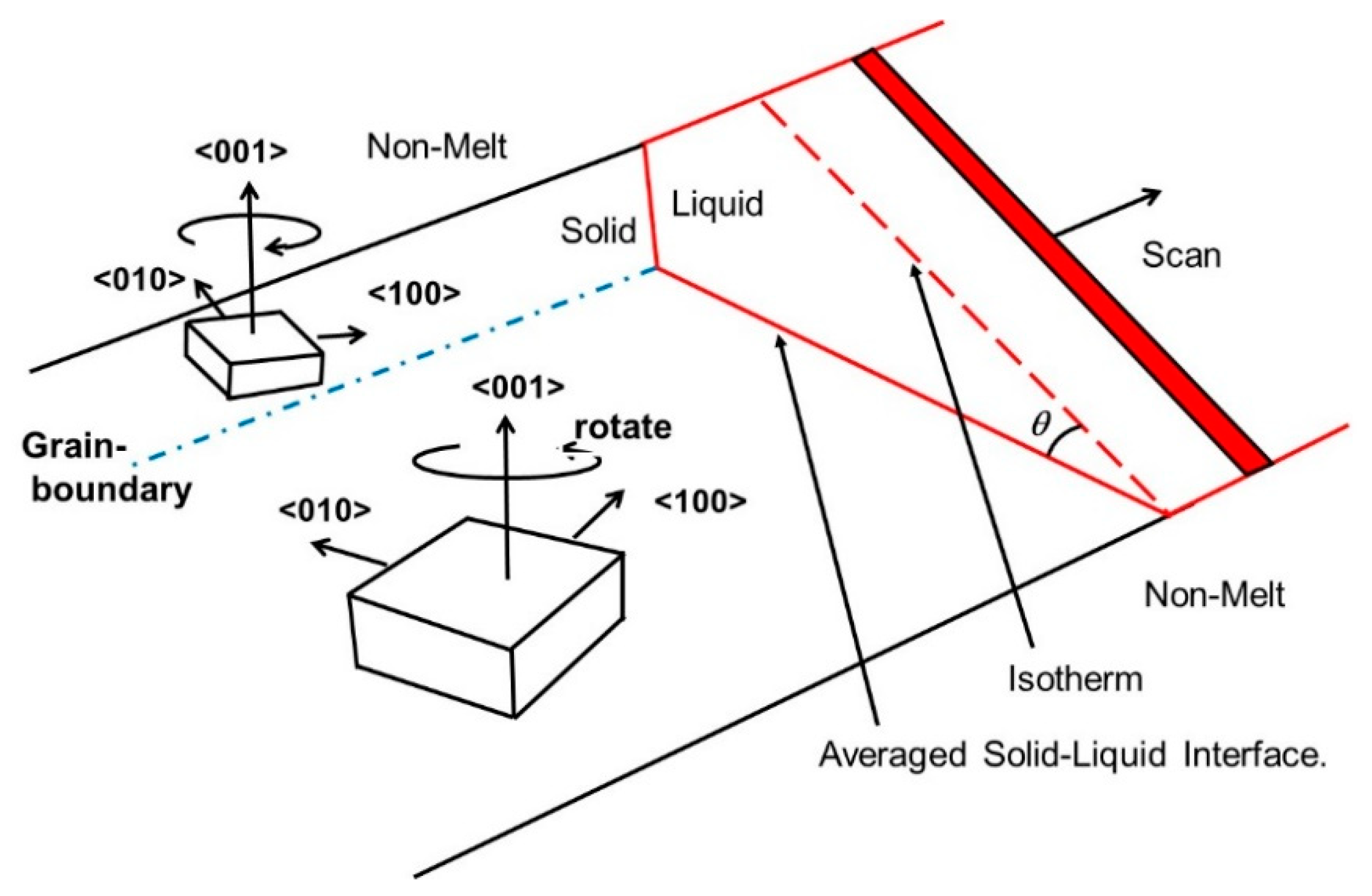
There are two kinds of laser crystallization methods on insulating substrate: the pulse excimer laser anneal (ELA), and the continuous-wave (CW)-laser lateral crystallization (CLC) [19]. Figure 2 shows a comparison of laser irradiation schemes between these two methods.
ELA has already been widely used commercially to make FPDs on glass or flexible substrates, but the commercially-used film crystallized by ELA with 17–20 shots (94%–95% overlapped scan) shows random crystalline orientations of small grains around 0.2–0.3 µmϕ [20], resulting in a lot of grain boundaries. The mobilities are limited around 150–250 cm2/Vs for n-MOS TFTs [7], and uniformities in electrical characteristics of TFT are poor [21]. Operational speed on panel is limited, and compensation circuit is necessary for organic light-emitting diode (OLED) pixels [21]. The CLC produces much larger elongated grains, such as ~10 μm wide and ~60 μm long, and higher mobilities of 400–500 cm2/Vs [22]; however, grain boundaries and random surface orientations are still observed in the Si films crystallized by the conventional CLC with the elliptical line beam for the non-patterned planar a-Si films [22,23,24,25]. Figure 3 shows a comparison of crystal growth directions and obtained grain boundary patterns of (a) ELA and (b) CLC; note that the magnifications of SEM images are different from each other. Figure 4 shows a comparison of the surface roughness obtained by laser crystallization of (a) ELA and (b) CLC; vertical magnifications are more enhanced than horizontal in the atomic force microscope (AFM) images, but the magnifications are the same between Figure 4a,b. The difference in brightness of the cross-sectional transmission electron microscope (TEM) images corresponds to different orientations of different grains, due to the bright field diffraction contrast. The rough surface of ELA films shown in Figure 4a increases the gate insulator leakage current and the threshold voltage fluctuation in TFTs.
So far, every laser crystallization method to produce grain-boundary-free films at a temperature less than 450 °C has failed to control crystal orientations of the crystallized region, and conversely, every method to obtain preferentially-oriented films has failed to eliminate grain boundaries from the crystallized region. The observation of the grain boundaries after the delineation by Secco etching of the crystallized film reveals that the grain boundaries can be eliminated from a defined area in the CW-laser crystallization, if isotherms are modulated by beam shaping [26,27,28,29], stripe cap patterning [30,31], Si island patterning [32,33,34], or substrate patterning [35]. The idea of these methods is to make the temperature of the controlled crystal growth region less than that of the peripheral regions, to suppress the disturbance to the growth region from the random nucleation at the peripheral. Even if a grain boundary happened to be formed in a central crystallized region, the grain boundary is swept outward with scan travel. However, it is difficult to realize the surface orientation control in addition to the grain boundary elimination by these isotherm modulations [29,31,34]. Yeh et al. reported a 1 mm-long grain-boundary-free Si stripe of 4 µm-width, having {100}-orientation in surface normal and {320}-orientation in scan direction, by crystallization with a chevron-shaped CW laser beam and a 300 nm-thick SiO2 cap [36]; however, they also reported orientation rotation with the scan travel in other scans at the same crystallization conditions in the same paper [36]. A wide {100} texture was also reported by CW-laser crystallization of a 10 µm-thick Si film at an elevated substrate at 700 °C [37,38], but these Si film thicknesses and substrate temperatures are too large to fabricate FETs or TFTs on glass or plastic substrate.
Preferentially {100}-oriented films can be also obtained at a room temperature substrate by overlapped pulse laser irradiations of more than 100 shots of ELA if the Si film thickness is less than 40 nm [39,40,41] or by overlapped CW laser scans of more than 10 scans [42,43,44], but the obtained films were full of grain boundaries [42,43,44]. Preferential {211} surface texture has been obtained by a double-line laser beam, but the film contained elongated parallel boundaries [45]. This {211} surface textured film changed to preferential {100} surface texture by six-time-overlapped scans, but the film still comprised grain boundaries [46,47,48].
This paper describes a recently found {100}-oriented grain-boundary-free film obtained by the unseeded CW-laser lateral crystallization with a single scan [44,49,50,51,52,53,54], with a highly top-flat line beam at the room temperature substrate. The grain boundary generation is suppressed in the crystallized region even with the simple line beam and without complicated beam shaping to grow the crystal from the central region outwards. This crystal growth means that {100}-textured crystal growth is possible, even at the room temperature substrate in the similar growth mechanism to that of ZMR realized at the elevated substrate temperature [11,12,13,14,15,16,17,18]. In this paper, grain boundaries are defined by the boundary whose rotation angle is larger than 15°, and sub-boundaries are defined by the boundary whose rotation angle is less than 15° [53,54,55], as shown in Figure 5. A grain, which is surrounded by grain boundaries, usually comprises some sub-grains and sub-boundaries [56].

2. Experimental

2.1. A New CW-Laser Lateral Crystallization (CLC) with a Highly Top-Flat Line Beam

A new CW-laser lateral crystallization (CLC) was performed by using a diode-pumped solid-state (DPSS) green laser with a wavelength of 532 nm at room temperature in air without seed, as shown in Figure 6. The equipment was built in our laboratory. A highly top-flat line beam was used, as shown in Figure 7 [44]. The homogenizer was also built in our laboratory. The beam size was 492 μm × 8 μm, but the narrower beam width of 5 μm was also used in the experiments investigating the effect of scan velocity. Samples were scanned using an electrically driven X-Y stage.

2.2. Sample Preparation and Characterization

A undoped 60 nm-thick a-Si was deposited on fused-quartz substrate after wet cleaning by using inductively coupled plasma chemical vapor deposition (ICP-CVD) with SiH4 at 250 °C and 6.7 Pa. An SiO2 cap was successively deposited from 86 to 184 nm thicknesses by ICP-CVD with tetraethoxysilane at 300 °C and 80 Pa. The deposition rate of SiO2 was 18 nm/min. After the dehydrogenation annealing at 500–550 °C for 1 h in nitrogen, the unseeded CLC was carried out at a laser power of 1.2–3.4 W with a scan velocity of 7.5–15 mm/s. The power density was 3–9 × 10⁴ W/cm2. Crystal quality was investigated by electron backscatter diffraction (EBSD) at an electron accelerating voltage of 15 kV and a tilt angle of 70°, using a Hitachi SU6600 scanning electron microscope equipped with an EBSD module from EDAX.

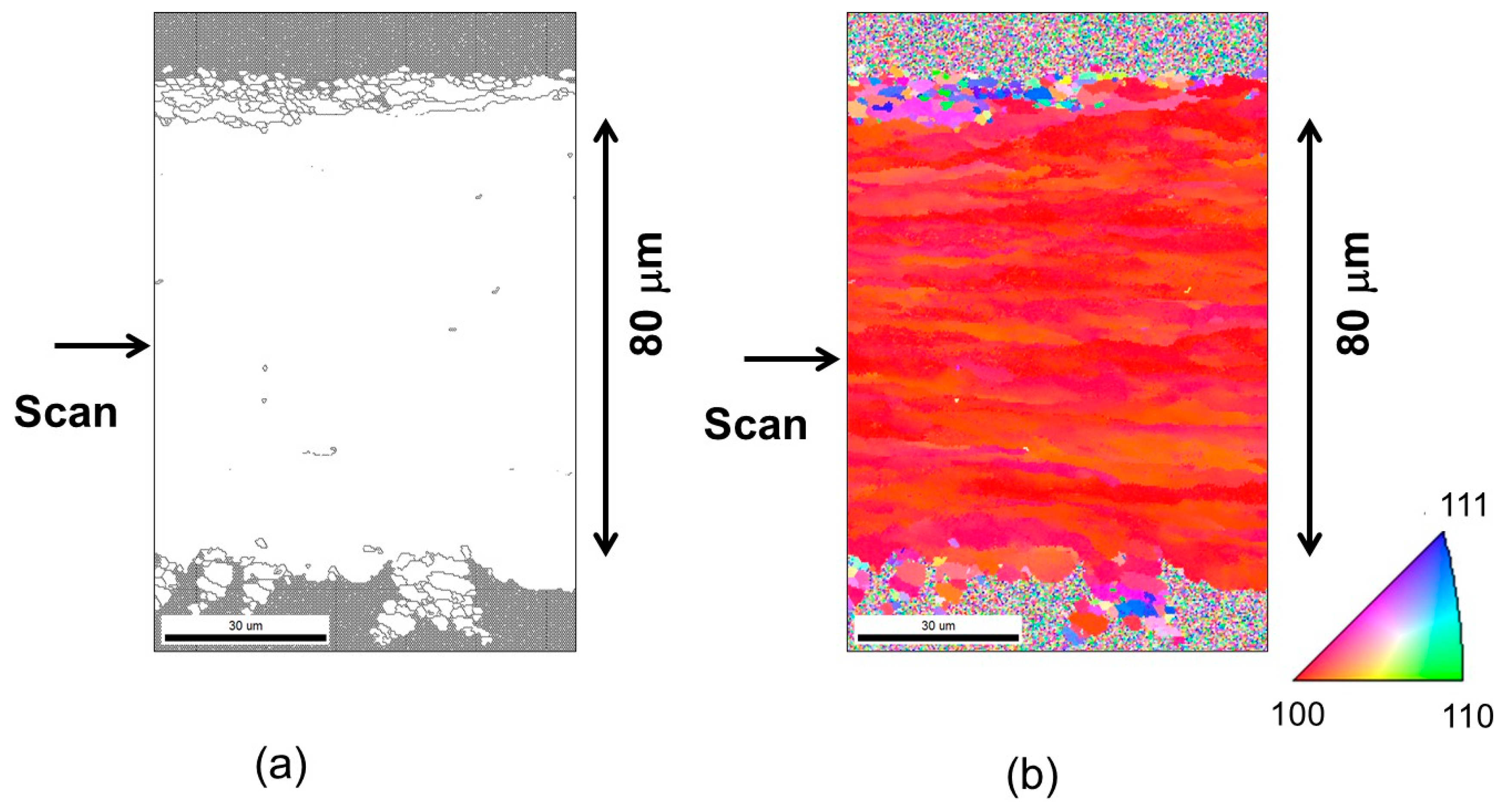
3. Laser Power Dependence of the Crystallographic Textures of the Crystallized Films

The laser power dependence of the crystallographic texture was studied in an area of 35 × 47 μm2, arbitrarily selected in the central region in the laser scan [44]. The crystallographic textures were investigated by EBSD. Three-dimensional orientations were detected by using EBSD, with an electron beam at a 15 nm spot size and a 300 nm step, at each point in the measured area. Figure 8 shows the surface normal texture diagram of the crystallized film as a function of laser power and the cap SiO2 thickness. Scan velocity was 15 mm/s. For each cap thickness, {100} textures were observed at the low power region near the lateral growth threshold, mixed textures were observed for the upper power, and agglomeration occurred for the further large power. Specifically, grain-boundary-free films were obtained in the vicinity of the lateral growth threshold. The power of the lateral growth threshold increased with the cap thickness from 86 to 184 nm, due to the decrease in the absorbed laser power in a-Si by the anti-reflection cap effect of the deposited SiO2 [49].
Figure 9 shows the EBSD inverse pole figure (IPF) maps in the directions of normal direction (ND), scan direction (SD), and transverse direction (TD) at the central area of 35 × 47 μm2 in the crystallized region, by a single CW laser scan at 123 nm cap thickness, 1.4 W power, and 15 mm/s scan velocity in air. The maps of the IPF ND, SD, and TD show color index to the orientations in the directions of ND, SD, and TD, respectively, at each point throughout the measured area. Textures of {100} are observed all over the area in all these three IPF maps of ND, SD, and TD. Figure 10 shows the grain boundary pattern. The grain boundaries are not observed, except for a tiny particle. Figure 11 shows the orientation distribution of the film. A total of 99.8% of the measured area is {100}-oriented in the surface normal direction within 10°.
When the laser power was increased to 1.6 W with the same cap thickness and the same scan velocity, the IPF ND texture remained in {100}, but in-plane SD and TD textures changed from {100} and domains parallel to the scan direction were formed, as shown in Figure 12 [44,49,53]. The orientations in SD and TD were orthogonal each other in each domain, and {100} ND was orthogonal to the orientations in SD and TD. This means that each domain had a single crystal rotated at a different angle around the <100> surface normal axis from the configuration of {100} ND, {100} SD, and {100} TD.
With a further increase in power, the mixed texture comprising small grains was observed in all the ND, SD, and TD, as shown in Figure 13. Domains having {211} ND, {110} SD, and {111} TD were observed as well [53]. The {211} ND domain in Figure 13 coincides with the extracted twin boundaries shown in Figure 14a. The directions of twin boundaries were almost parallel (0–10°) to the scan direction, as shown in Figure 14b.

4. Crystal Growth Model as a Function of the Laser Power

Figure 15 shows the schematic view of the solid-liquid interface at the low laser power in the vicinity of the lateral growth threshold [53] resulting from Figure 9. The {100} orientation is formed in the directions of SD and TD, in addition to ND. A single straight line of averaged solid-liquid interface is formed in the direction vertical to the scan direction. The crystal orientations of this growth are very symmetrical.
When the laser power is increased from the lateral growth threshold but is still low enough, domains having tilted solid-liquid interface are generated, having the in-plane SD and TD orientations rotated from {100} SD and ND, keeping the {100} ND, as shown in Figure 16 [53]. The averaged sold-liquid interfaces are also rotated at θ and a grain boundary is formed parallel to the scan direction between two domains.
The sole observation of {100} ND texture of a crystallized region does not always mean the region is grain-boundary-free; however, when we observe the symmetrical textures of {100} ND, {100} SD, and {100} TD at the same time in a region, we can regard the region as {100}-oriented grain-boundary-free.
With further increased power, stable solid-liquid interfaces are no more maintained, and small grains with different orientations are generated. Domains of twins are observed as well. The twin boundary generation is explained by two steps: first, the in-plane rotation of the averaged solid-liquid interface is induced, and secondly, the deformation twinning is induced by the compressive stress in the crystallized film at the onset of solidification before cooling down [53]. The twin is not formed in the crystal of {100} SD, but is formed in the crystal of {110} SD. The experimentally observed direction of twins were almost parallel (0–10°) to the scan direction, as shown in Figure 14. If the twin is formed in the crystal of {100} SD, the twin direction forms an angle of 45° with the scan direction, because the twin boundary is formed by glides of the partial dislocations on the {111} plane. This agrees well with the difference in calculated Schmid factors between crystals of {100} SD and {110} SD [53].

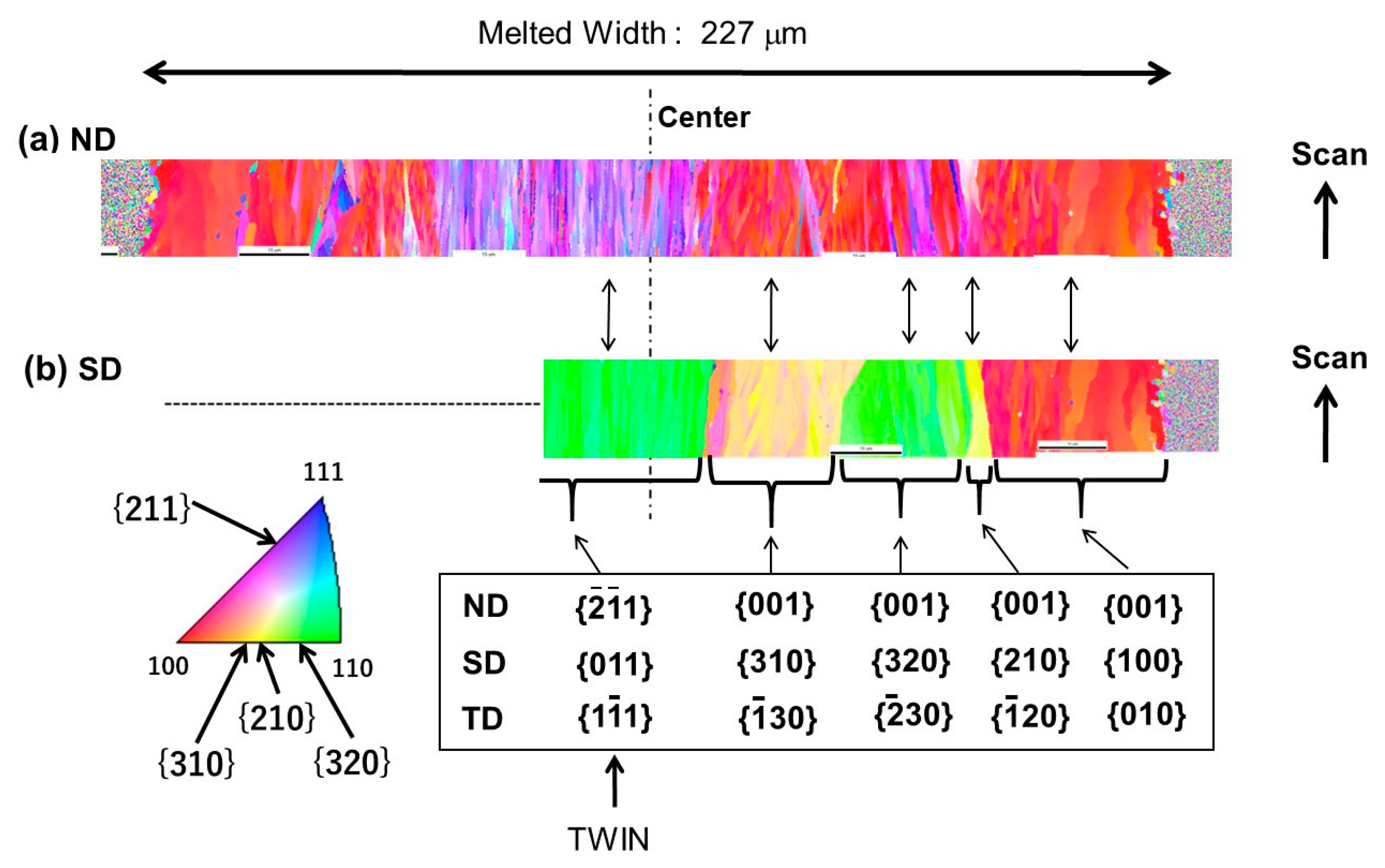
5. Global Texture Throughout the Melted Width

The {100} orientations in the directions of ND, SD, and TD were obtained throughout the melted width, except the tiny edge regions at the low laser power in the vicinity of the lateral growth threshold [50]. No grain boundary was observed all over the melted width except the edge regions, as shown in Figure 17a. The {100} ND orientation was also observed except in the edge regions, as shown in Figure 17b. The {100} SD and TD orientations were also observed in the same region. The width of this {100}-oriented grain-boundary-free film is 80 μm. The width of 120 μm was obtained as well [52].
Figure 18 shows the global textures of the crystallized film throughout the melted width at a higher power condition [53]. The absorbed power of Figure 18 is greater than that of Figure 17, because of the difference in the cap thickness even with the same irradiated power. There are various domains due to the temperature distribution induced by lateral thermal diffusion even with a top-flat line beam profile. Near the edge of the melted width, {100}-oriented grain-boundary-free domains are produced, similar to Figure 9. In the central region of the melted width, there are in-plane tilted domains such as those observed in Figure 12, and the twinned domain with the same textures of {211} ND, {110} SD, and {111} TD, similar to those observed in Figure 13.

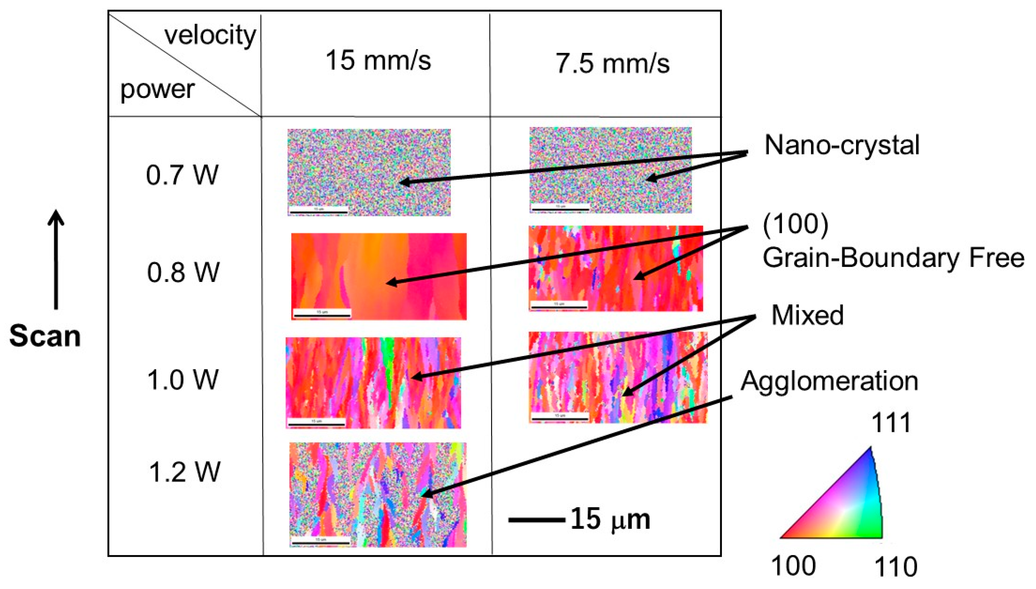
6. Effect of Scan Velocity on the (100) Texture

Figure 19 shows the effect of scan velocity on surface textures of the lateral growth [50]. The {100} surface texture in the lateral growth is observed, even in a 7.5 mm/s scan velocity. The laser power window to obtain {100} grain-boundary-free texture becomes wider with increasing scan velocity.

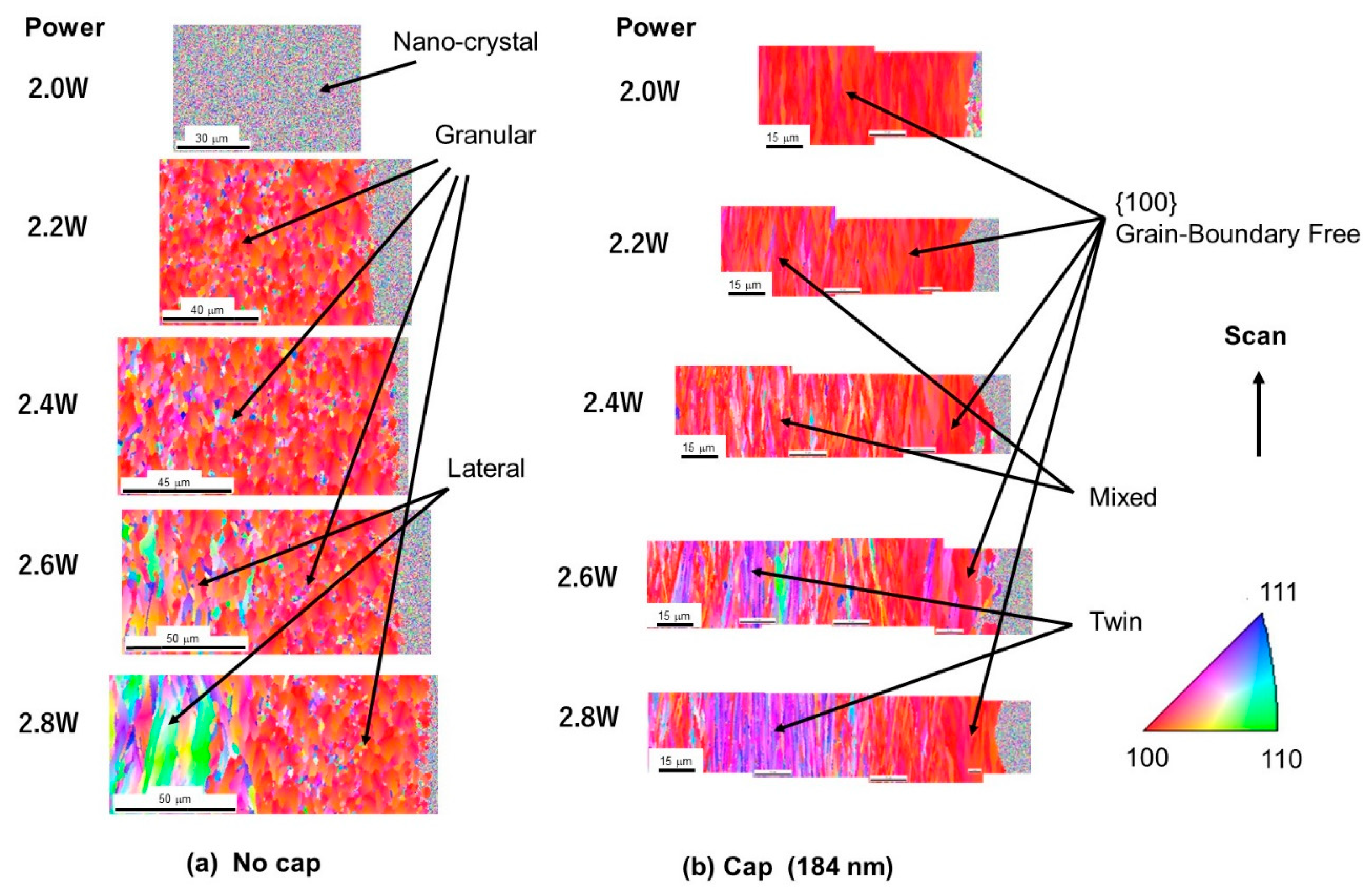
7. Cap Effect to Produce the {100} Texture

The effects of the SiO2 cap on the surface textures are shown in Figure 20. The SiO2 cap is essential to obtain the {100} grain-boundary-free lateral growth [54]. The lateral growth threshold power with the cap is smaller than that without the cap. This is explained by the anti-reflection effect of the cap [49].
Figure 20a shows the texture’s dependence on laser power for the samples without the cap. Nanocrystals are observed at 2.0 W, and granular grains at powers from 2.2 to 2.4 W. The granular grains are preferentially {100} ND-oriented, but many smaller grains of {110} or {111} ND are observed as well. It should be noted that the random IPF ND textures are generated in the lateral growth region observed at the middle of melted width at 2.6 and 2.8 W powers. The textures at the edges remain granular at 2.6 and 2.8 W, due to the decrease in temperature due to lateral thermal diffusion.
Figure 20b shows the texture dependence on laser power for the capped sample. All the textures show lateral growth at powers from 2.0 to 2.8 W, and {100} ND texture is observed around the lateral growth threshold of 2.0 W, all over the melted width. The IPF ND map changes to the mixed texture from 2.2 and 2.4 W in the central region of the melted width. The {100} textured grain-boundary-free regions are observed at 2.2–2.8 W in the side edges, and the deformation twinning [53] occurs at 2.6 and 2.8 W in the central region.

8. Multiple Overlapped Scan Effect on the {100} Texture

Overlapped scans make the preferentially {100} textured film but leave grain boundaries in the film [44]. Figure 21a shows IPF ND texture at the higher laser power condition with a single scan. Mixed texture and twinned regions are observed. Figure 21b,c show the IPF ND maps after (b) 5 times, and (c) 80 times scans at the same place with the same laser conditions. The {211} ND twin region disappears with 5 times scans, and preferentially {100}-oriented ND texture is obtained with 80 times scans, but grain boundaries are not removed from the overlapped scan area, even with 80 times scan.

9. Discussion

We have found that a simple line beam can realize the symmetrical {100} ND, SD, and TD crystal growth. The {100} ND orientation is realized by the minimum interfacial energy between Si{100} and SiO2 [11]. The grains with in-plane {100} SD orientation dominate [49,53,54] due to the geometry selection [57], because of the fastest growth direction of <100> in Si [17,58,59,60]. Once the {100} SD is realized, it is maintained. But if the power density varies or fluctuates, the solid-liquid interface will no longer be stably maintained. This is the reason why we must use a highly top-flat beam to obtain the {100} ND, SD, and TD crystal growth.
The geometry selection will not work effectively in very narrow and thin wires like the experiments of Yeh et al. [29,36]. The nucleus with the {100} SD orientation is not always included in the nuclei randomly nucleated at the scan starting point in a limited space for nucleation if the crystallization stripe is narrow and thin. On the other hand, the geometry selection works well for the wider linear beam even in thin film, like our study [49,50,51,52,53,54], or for thick film, like the experiments of Kühnapfel et al. [37,38].
The in-plane domain rotation observed at a higher power is explained by the in-plane rotation of averaged solid-liquid interface parting from the isotherm plane [53].The granular grains observed at the power lower than the lateral growth threshold are generated by the vertical growth due to the solid-liquid interface tilted horizontally to the substrate [54].
The transition of surface normal textures in CLC films from the {100} to the {211} at high laser power is induced by the in-plane rotation of the solid-liquid interface and the successive deformation twinning by volume expansion stress [53]. We suppose that the {211}-textured domain obtained with the double-line beam by Kuroki [45] was not governed at initial crystal nucleation [45], but was also produced by the deformation twinning after the crystal growth, in the same way as we observed in our study with the highly top-flat single-line beam [53].

10. Conclusions

It has been found that the {100}-oriented grain-boundary-free film is obtained by the CW-laser lateral crystallization when the following conditions are satisfied:
  • Simple but highly uniform top-flat line beam.
  • SiO2 cap.
  • Low laser power density in the vicinity of the lateral growth threshold.
  • Single scan crystallization.
This crystallization was carried out simply on a room temperature substrate in air without seed, and the crystallization equipment was simple as well. A wide {100}-oriented grain-boundary-free stripe of more than 120 μm width was obtained. The increased scan velocity makes the optimum power window wide further to produce the {100} crystal growth. A SiO2 cap is essential to get {100} ND to reduce the interface energy. The sufficiently wide melted width is substantial to get {100} SD by the mechanism of the geometry selection.

Author Contributions

Conceptualization, methodology, analysis, and writing, N.S.; investigation, M.A.; resources, Y.U.; funding acquisition, J.G., S.S. All authors have read and agreed to the published version of the manuscript.

Funding

This research received no external funding.

Conflicts of Interest

The authors declare no conflicts of interest.

References

  1. Sasaki, N. Feasibility of 3D untegration. Eur. Trans. Telecommun. Related Tech. 1990, 1, 137. [Google Scholar] [CrossRef]
  2. Batude, P. 3D Sequential integration. In Proceedings of the IEEE IEDM, Washington, DC, USA, 7−11 December 2019. [Google Scholar]
  3. Wager, J.F. Oxide TFTs: A progress report. Inf. Disp. 2016, 32, 16. [Google Scholar] [CrossRef]
  4. Facchetti, A.; Hsiao, C.-C.; Huitema, E.; Inagaki, P. Enabling wearable and other novel applications through flexible TFTs. Inf. Disp. 2016, 32, 6. [Google Scholar] [CrossRef]
  5. Sasaki, N.; Kawamura, S.; Iwai, T.; Mukai, R.; Nakano, M.; Takagi, M. 3-dimensional IC’s Fabricated by using Ar+ Laser Recrystallization. In Proceedings of the 15th Conf. Solid State Devices and Materials, Late News, A-3-7LN, Tokyo, Japan, 30 August–1 September 1983; Kawamura, S., Sasaki, N., Iwai, T., Mukai, R., Nakano, M., Takagi, M., Eds.; IEEE IEDM: Washington, DC, USA, 5–7 December 1983; p. 364. [Google Scholar]
  6. Sasaki, N.; Togei, R. Effect of silicon film thickness on thershold voltage of SOS-MOSFETs. Solid-St. Electron. 1979, 22, 417. [Google Scholar] [CrossRef]
  7. Hara, A.; Takeuchi, F.; Sasaki, N. Mobility Enhancement limit of excimer-laser-crystallized polycrystalline silicon thin film transistors. J. Appl. Phys. 2002, 91, 708. [Google Scholar] [CrossRef]
  8. Sasaki, N. Change of Si-SiO2 interface charge by BT treatment. Jpn. J. Appl. Phys. 1973, 12, 1458. [Google Scholar] [CrossRef]
  9. Colman, B.; Bate, R.T.; Mize, J.P. Mobility anisotropy and piezoresistance in silicon p-type inversion layers. J. Appl. Phys. 1968, 39, 1923. [Google Scholar] [CrossRef]
  10. Sato, T.; Takeishi, Y.; Hara, H. Mobility anisotropy of electrons in inversion layers on oidized silicon surfaces. Phys. Rev. 1971, 4, 1950. [Google Scholar] [CrossRef]
  11. Geis, M.W.; Smith, H.I.; Tsaur, B.Y.; Fan, J.C.C.; Silversmith, D.J.; Mountain, R.W. Zone-melting recrystallization of Si films with a movable-strip-heater oven. J. Electrochem. Soc. 1982, 129, 2812. [Google Scholar] [CrossRef]
  12. Tsaur, B.-Y.; Fan, J.C.C.; Geis, M.W.; Silversmith, D.J.; Mountain, R.W. Effects of subgrain boundaries on carrier transport in zone-melting-recrystallized Si films on SiO2-coated Si substrates. IEEE Elec. Dev. Lett. 1982, EDL-3, 79. [Google Scholar] [CrossRef]
  13. Geis, M.W.; Smith, H.I.; Silversmith, D.J.; Mountain, R.W.; Thompson, C.V. Solidification-front modulation to entrain subboundaries in zone-melting recrystallization of Si on SiO2. J. Electrochem. Soc. 1983, 130, 1178. [Google Scholar] [CrossRef]
  14. Pfeiffer, L.; Paine, S.; Gilmer, G.H.; van Saarloos, W.; West, K.W. Pattern formation resulting from faceted growth in zone-melted thin films. Phys. Rev. Lett. 1985, 54, 1944. [Google Scholar] [CrossRef] [PubMed] [Green Version]
  15. Chen, C.K.; Geis, M.W.; Finn, M.C.; Tsaur, B.Y. New capping technique for zone-melting recrystallization of silicon-on-insulator films. B.-Y. Appl. Phys. Lett. 1986, 48, 1300. [Google Scholar] [CrossRef]
  16. Geis, M.W.; Smith, H.I.; Chen, C.K. Characterization and entrainment of subboundaries and defect trails in zone-melting recrystallized Si films. J. Appl. Phys. 1986, 60, 1152. [Google Scholar] [CrossRef]
  17. Pfeiffer, L.; Gelman, A.E.; Jackson, K.A.; West, K.W.; Batstone, J.L. Subboundary-free zone-melt recrystallization of thin film silicon. Appl. Phys. Lett. 1987, 51, 1256. [Google Scholar] [CrossRef]
  18. Miaoulis, I.N.; Wong, P.Y.; Lipman, J.D.; Im, J.S. Thermal modeling of zone-melting-recrystallization processsing of silicon-on-insulator film structures. J. Appl. Phys. 1991, 69, 7273. [Google Scholar] [CrossRef]
  19. Sasaki, N.; Hara, A.; Takeuchi, F.; Mishima, Y.; Kakehi, T.; Yoshino, K.; Takei, M. High Throughput CW-Laser Lateral Crystallization for Low-Temperature Poly-Si TFTs and Fabrication of 16 Bit SRAMs and 270 MHz Shift Registers; SID: Boston, MA, USA, 2002; p. 154. [Google Scholar]
  20. Valletta, A.; Gaucci, P.; Mariucci, L.; Fortunato, G.; Brotherton, S.D. Kink effect in short-channel polycrystalline silicon thin-film transistors. Appl. Phys. Lett. 2004, 85, 3113. [Google Scholar] [CrossRef]
  21. Cunningham, K.L. A Process for using oxide TFTs over LTPS TFTs for OLED-TV manufacturing. Inf. Disp. 2015, 31, 28. [Google Scholar] [CrossRef]
  22. Hara, A.; Takei, M.; Takeuchi, F.; Suga, K.; Yoshino, K.; Chida, M.; Kakehi, T.; Ebiko, Y.; Sano, Y.; Sasaki, N. High performance low temperature polycrystalline silicon thin film transistors on non-alkaline glass produced using diode pumped solid state continuous wave laser lateral crystallization. Jpn. J. Appl. Phys. 2004, 43, 1269. [Google Scholar] [CrossRef]
  23. Matsumura, M.; Hatano, M.; Kaitoh, T.; Ohkura, M. Subthreshold properties of TFTs with laser-crystallized laterally grown polysilicon layers. IEEE Electron Device Lett. 2006, 27, 278. [Google Scholar] [CrossRef]
  24. Chou, C.-H.; Lee, I.-C.; Yang, P.-Y.; Hu, M.-J.; Wang, C.-L.; Wu, C.-Y.; Chien, Y.-S.; Wang, K.-Y.; Cheng, H.-C. Effects of crystallization mechanism on the electrical characteristics of green continuous-wave-laser-crystallized polycrystalline silicon thin film transistors. Appl. Phys. Lett. 2013, 103, 053515. [Google Scholar] [CrossRef]
  25. Jin, S.; Choe, Y.; Lee, S.; Kim, T.-W.; Mativenga, M.; Jang, J. Lateral grain growth of amorphous silicon films with wide thickness range by Blie laser annealing and application to high performance poly-Si TFTs. J. IEEE Electron Dev. Lett. 2016, 37, 291. [Google Scholar] [CrossRef]
  26. Stultz, T.J.; Gibbons, J.F. The use of beam shaping to achieve large-grain CW laser-recrystallized polysilicon on amorphous substrate. Appl. Phys. Lett. 1981, 39, 498. [Google Scholar] [CrossRef]
  27. Kawamura, S.; Sakurai, J.; Nakano, M.; Takagi, M. Recrystallization of Si on amorphous substrates by doughnut-shaped CW Ar laser beam. Appl. Phys. Lett. 1982, 40, 394. [Google Scholar] [CrossRef]
  28. Sasaki, N.; Mukai, R.; Izawa, T.; Nakano, M.; Takagi, M. Melt-width enhancement in the recrystallization of polycrystalline silicon-on-insulator by twin-laser-beam-induced substrate interheating. Appl. Phys. Lett. 1984, 45, 1098. [Google Scholar] [CrossRef]
  29. Yeh, W.; Yamazaki, S.; Ishimoto, A.; Morito, S. Single-grain growth in Si film by chevron-shaped CW laser beam scanning. Appl. Phys. Express 2016, 9, 025503. [Google Scholar] [CrossRef]
  30. Colinge, J.P.; Demoulin, E.; Bensahel, D.; Auvert, G. Use of selective annealing for growing very large grain silicon on insulator films. Appl. Phys. Lett. 1982, 41, 346. [Google Scholar] [CrossRef]
  31. Sugahara, K.; Kusunoki, S.; Inoue, Y.; Nishimura, T.; Akasaka, Y. Orientation control of the silicon film on insulattor by laser recrystallization. J. Appl. Phys. 1987, 62, 4178. [Google Scholar] [CrossRef]
  32. Biegelson, D.K.; Johnson, N.M.; Bartelink, D.J.; Moyer, M.D. Laser-induced crystallization of silicon islamds on amorphous substrates: Multilayer Structures. Appl. Phys. Lett. 1981, 38, 150. [Google Scholar] [CrossRef]
  33. Mukai, R.; Sasaki, N.; Iwai, T.; Kawamura, S.; Nakano, M. Single crystalline Si islands on an amorphous insulating layer recrystallized by an indirect laser heating technique for three-dimensional integrated circuits. Appl. Phys. Lett. 1984, 44, 994. [Google Scholar] [CrossRef]
  34. Mukai, R.; Sasaki, N.; Nakano, M. Study of the laser-recrystllized film with a control of grain boundary location by using surrounding antireflection cap method. J. Electron. Mater. 1986, 15, 339. [Google Scholar] [CrossRef]
  35. Kawamura, S.; Sasaki, N.; Nakano, M.; Takagi, M. Laser recrystallization of si over sio2 with a heat-sink structure. J. Appl. Phys. 1984, 55, 1607. [Google Scholar] [CrossRef]
  36. Yeh, W.; Shirakawa, T.; Pham, A.H.; Morito, S. Lateral growth of a twin-free si stripe longer than 1 mm as a result of rotation suppression. Jpn. J. Appl. Phys. 2019, 58, SBBJ06. [Google Scholar] [CrossRef]
  37. Kühnapfel, S.; Nickel, N.H.; Gall, S.; Klaus, M.; Genzel, C.; Rech, B.; Amkreutz, D. Preferentiall {100} Grain orientation in 10 microeter-thick laser crystallized multicrystalline silicon on glass. Thin Solid Films 2015, 576, 68. [Google Scholar] [CrossRef]
  38. Kühnapfel, S.; Gall, S.; Klaus, M.; Rech, B.; Amkreutz, D. Towards monocrystalline silicon thin films grown on glass by liquid phase crystallization. Solar Energy Mater. Solar Cells 2015, 140, 86. [Google Scholar] [CrossRef]
  39. Gosain, D.P.; Machida, A.; Fujino, T.; Hitsuda, Y.; Nakano, K.; Sato, J. Formation of (100)-textured Si film using an excimer laser on a glass substrate. Jpn. J. Appl. Phys. 2003, 42, L135. [Google Scholar] [CrossRef]
  40. He, M.; Ishihara, R.; Metselaar, W.; Beenakker, K. <100>-Textured self-assembled square-shaped polycrystalline silicon grains by multiple shot excimer laser crystallization. J. Appl. Phys. 2006, 100, 083103. [Google Scholar] [CrossRef] [Green Version]
  41. Weizman, M.; Klimm, C.; Nickel, N.H.; Rech, B. Origin of preferential grain orientation in excimer laser-induced crystallization of silicon thin films. Appl. Phys. Lett. 2012, 100, 161906. [Google Scholar] [CrossRef]
  42. Im, J.S.; Chahal, M.; van der Wilt, P.C.; Chung, U.J.; Ganot, G.S.; Chitu, A.M.; Kobayashi, N.; Ohmori, K.; Limanov, A.B. Mixed-phase solidification of thin si films on SiO2. J. Cryst. Growth 2010, 312, 2775. [Google Scholar] [CrossRef]
  43. Jin, S.; Hong, S.; Mativenga, M.; Kim, B.; Shin, H.H.; Park, J.K.; Kim, T.-W.; Jang, J. Low temperature polycrystalline silicon with single orientation on glass by blue laser annealing. Thin Solid Films 2016, 616, 838. [Google Scholar] [CrossRef]
  44. Sasaki, N.; Nieda, Y.; Hishitani, D.; Uraoka, Y. Growth of Highly-Oriented LTPS Films by CW Laser Lateral Crystalliation; SID: San Francisco, CA, USA, 22–27 May 2016; p. 1317. [Google Scholar]
  45. Kuroki, S.-I.; Kawasaki, Y.; Fujii, S.; Kotani, K.; Ito, T. Seed-free fabrication of highly bi-axially oriented poly=Si thin films by continuous-wave laser crystallization with double-line beams. J. Electrochem. Soc. 2011, 158, H924. [Google Scholar] [CrossRef]
  46. Nguyen, T.T.; Hiraiwa, M.; Kuroki, S.-I. Ultrahigh-performance (100)-oriented polycrystalline silicon thin-film transistors and their microscopic crystal structures. Appl. Phys. Express 2017, 10, 056501. [Google Scholar] [CrossRef]
  47. Nguyen, T.T.; Hiraiwa, M.; Koganezawa, T.; Yasuno, S.; Kuroki, S.-I. Formation of (100)-oriented large polycrystalline silicon thin films with multiline beam continuous-wave laser lateral crystallization. Jpn. J. Appl. Phys. 2018, 57, 031302. [Google Scholar] [CrossRef]
  48. Nguyen, T.T.; Kuroki, S.-I. Dependence of thin film transistor characteristics on low-angle grain boundaries of (100)-oriented polycrystalline silicon thin films. Jpn. J. Appl. Phys. 2019, 58, SBBJ08. [Google Scholar] [CrossRef]
  49. Sasaki, N.; Nieda, Y.; Hishitani, D.; Uraoka, Y. Power dependence of orientation in low-temperature poly-Si lateral grains crystallized by a continuous-wave laser scan. Thin Solid Films 2017, 631, 112. [Google Scholar] [CrossRef]
  50. Sasaki, N.; Arif, M.; Uraoka, Y. Folded Pixel Circuits Design in Grain-Boundary Free (100) Oriented Ltps Stripes Fabricated by Selective Cw-Laser Lateral Crystallization; SID: Los Angeles, CA, USA, 20–25 May 2018; p. 755. [Google Scholar]
  51. Sasaki, N.; Arif, M.; Uraoka, Y. Effect of Laser Power on the Surface Texture Transition of the Thin Si-Films from Grain-Boundary Free (100) to Twinned (211) in CW Laser Laeral Crystallization; Int. Conf. Solid State Devices and Materials: Tokyo, Japan, 2018; N-2-02. [Google Scholar]
  52. Sasaki, N.; Arif, M.; Uraoka, Y. Characterization of the Grain-Boundary Free (100) Si Thin-Films Obtained by CW-Laser-Lateral Crystallization at Room Temperature in Air; IEEE EDTM: Singapore, 12–15 March 2019; ID160. [Google Scholar]
  53. Sasaki, N.; Arif, M.; Uraoka, Y. Transition mechanism of the Thin Si-films obtained by the CW laser lateral crystallization from the grain-boundary free highly {100} oriented crystal to the twinned {211} crystal depending on the lase power. Jpn. J. Appl. Phys. 2019, 58, SBBJ02. [Google Scholar] [CrossRef]
  54. Sasaki, N.; Arif, M.; Uraoka, Y. Effect of surface tension on crystal growth of Si thin films by a continuous-wave laser lateral crystallization. Appl. Phys. Express 2019, 12, 055508. [Google Scholar] [CrossRef]
  55. Kaneko, H. Tetsu-to-Hagane. Structure of Grain Boundary. Iron Steel 1970, 56, 622. (In Japanese) [Google Scholar] [CrossRef]
  56. Hirth, J.P.; Lothe, J. Grain Boundaries. Theory of Dislocations, 2nd ed.; Krieger Pub. Co.: Malabar, FL, USA, 1982; p. 697. [Google Scholar]
  57. Kolmogorov, A.N. On the “geometrical selection” of crystals. Dokl. Acad. Nauk SSSR 1949, 65, 681. [Google Scholar]
  58. Gilmer, G.H. Ising model simulations of impurity trapping in silicon. Mater. Res. Soc. Symp. Proc. 1983, 13, 249. [Google Scholar] [CrossRef]
  59. Csepregi, L.; Kennedy, E.F.; Mayer, J.W. Substrate-orientation dependence of the epitaxial regrowth rate from Si-implanted amorphous Si. J. Appl. Phys. 1978, 49, 3906. [Google Scholar] [CrossRef]
  60. Ho, K.T.; Suni, I.; Nicolet, M.-A. Substrate orientation dependence of enhanced epitaxial regrowth of silicon. J. Appl. Phys. 1984, 56, 1207. [Google Scholar] [CrossRef] [Green Version]
Figure 1. The first fabrication of monolithic three-dimensional integrations (3D IC). The n-MOS silicon on insulator (SOI) transistor is stacked over bulk p-MOS transistor. (a) Schematic illustration of the 3D inverter. (b) Cross-sectional SEM view. After Sasaki et al. [5].
Crystals 10 00405 g001
Figure 2. Comparison of laser irradiation between (a) excimer laser anneal (ELA) and (b) continuous-wave (CW)-laser lateral crystallization (CLC). (a) ELA: Pulse XeCl excimer laser, λ = 308 nm, and power fluctuation ~ ±10%. (b) CLC: CW laser (diode-pumped solid-state (DPSS)), λ = 532 nm, and power fluctuation < ±1%.
Crystals 10 00405 g002
Figure 3. SEM pictures after the delineation of grain boundaries by Secco etching. Crystal growth directions and grain boundary patterns are shown. (a) A 400 nm-thick buffer SiO2 and a successive 45 nm-thick a-Si were deposited by PE-CVD on a glass substrate. ELA was carried out at an energy density of 450 mJ/cm2 and an irradiation of 20 shots for each point. (b) A 400 nm-thick buffer SiO2 and a successive 150 nm-thick a-Si were deposited on a glass substrate. CLC was carried out at 10 W power and 50 cm/s scanning velocity with an elliptical line beam. Beam size was 400 μm × 20 μm.
Crystals 10 00405 g003
Figure 4. Surface roughness. AFM and cross-sectional TEM images of the crystallized films. (a) crystallized by ELA. (b) crystallized by CLC. The brightness change in TEM corresponds to crystal orientation change. Conditions of sample fabrication and crystallization are the same as those in Figure 3.
Crystals 10 00405 g004
Figure 5. Definition of grain boundary and sub-boundary.
Crystals 10 00405 g005
Figure 6. Schematic view of the new CLC equipment.
Crystals 10 00405 g006
Figure 7. Beam profile of highly top-flat line beam (arbitrary unit). After Sasaki et al. [44].
Crystals 10 00405 g007
Figure 8. Phase diagram of the {100} texture and mixed texture. The scan velocity was 15 mm/s. After Sasaki et al. [44].
Crystals 10 00405 g008
Figure 9. {100} textures of inverse pole figure (IPF) maps for all three directions of (a) normal direction (ND), (b) scan direction (SD), and (c) transverse direction (TD), obtained at a low laser power in the vicinity of the lateral growth threshold. The SiO2 cap thickness was 123 nm, and the power was 1.4 W. The scan velocity was 15 mm/s. After Sasaki et al. [44].
Crystals 10 00405 g009
Figure 10. EBSD map of grain boundary pattern at the area shown in Figure 9. The SiO2 cap thickness was 123 nm, and the power was 1.4 W. The scan velocity was 15 mm/s. After Sasaki et al. [49].
Crystals 10 00405 g010
Figure 11. Distribution of surface direction around {100}. (a) IPF plot and (b) surface direction chart. 99.8% of the crystallized region is {100} ND-oriented within 10°. The SiO2 cap thickness was 123 nm, and the power was 1.4 W. The scan velocity was 15 mm/s. After Sasaki et al. [52].
Crystals 10 00405 g011
Figure 12. IPF maps of the crystallized film at an increased effective laser power a little from the lateral growth threshold; (a) normal direction, (b) scan direction, and (c) transverse direction. The SiO2 cap thickness was 123 nm, and the power was 1.6 W. The scan velocity was 15 mm/s. After Sasaki et al. [53].
Crystals 10 00405 g012
Figure 13. IPF maps of the crystallized film at a high effective laser power; (a) normal direction, (b) scan direction, and (c) transverse direction. The SiO2 cap thickness was 183 nm, and the power was 2.6 W. The scan velocity was 15 mm/s. After Sasaki et al. [53].
Crystals 10 00405 g013
Figure 14. EBSD maps of (a) twin boundaries, and (b) the lines fitted to the twin boundaries. The same area of the sample shown in Figure 13 was investigated. The SiO2 cap thickness was 183 nm, and the power was 2.6 W. The scan velocity was 15 mm/s. After Sasaki et al. [53].
Crystals 10 00405 g014
Figure 15. Crystal growth at the low power in the vicinity of the lateral growth threshold. After Sasaki et al. [53].
Crystals 10 00405 g015
Figure 16. Crystal growth at the low laser power but deviated from the lateral growth threshold power. After Sasaki et al. [53].
Crystals 10 00405 g016
Figure 17. Global extension of the {100}-oriented grain-boundary-free film. The SiO2 cap thickness was 123 nm, and the power was 1.4 W. (a) Grain boundary map, and (b) IPF ND map. The scan velocity was 15 mm/s. After Sasaki et al. [50].
Crystals 10 00405 g017
Figure 18. Global textures of the crystallized film at a higher laser power. (a) IPF ND map, and (b) IPF SD map. The SiO2 cap thickness was 84 nm, and the power was 1.4 W. The scan velocity was 15 mm/s. After Sasaki et al. [53].
Crystals 10 00405 g018
Figure 19. Comparison of {100} crystal growth between 7.5 and 15 mm/s scan velocities. The beam width was decreased to 5 μm in this experiment for both scan velocities. The cap oxide thickness was 87 nm. After Sasaki et al. [50].
Crystals 10 00405 g019
Figure 20. Effects of SiO2 cap to grow {100}-oriented films. EBSD IPF ND maps are shown as a function of laser power; (a) without cap, and (b) with cap of 184 nm. In (a), natural oxide on the surface was etched off by the buffered HF solution just before the crystallization. The laser scan velocity was 15 mm/s. After Sasaki et al. [54].
Crystals 10 00405 g020
Figure 21. Effects of multiple overlapped scans on surface textures. IPF ND maps of (a) 1 time, (b) 5 times, and (c) 80 times overlapped scans, at the same laser crystallization conditions. The cap oxide was 86 nm thick, the power was 1.4 W, and the scan velocity was 15 mm/s. After Sasaki et al. [4].
Crystals 10 00405 g021

