Article

Determination of the Complex Dielectric Function of Ion-Implanted Amorphous Germanium by Spectroscopic Ellipsometry

1
Institute of Technical Physics and Materials Science, Centre for Energy Research, Konkoly Thege Miklós Rd. 29-33, H-1121 Budapest, Hungary
2
Institute for Particle and Nuclear Physics, Wigner Research Centre for Physics, Konkoly Thege Miklós Rd. 29-33, H-1121 Budapest, Hungary
3
Institute of Microelectronics and Technology, Óbuda University, P.O. Box 112, 1431 Budapest, Hungary
*
Author to whom correspondence should be addressed.
These authors contributed equally to this work.
Coatings 2020, 10(5), 480; https://doi.org/10.3390/coatings10050480
Submission received: 9 April 2020 / Revised: 8 May 2020 / Accepted: 11 May 2020 / Published: 16 May 2020
(This article belongs to the Special Issue Structure and Phase Transformations in Thin Films)

Abstract

:
Accurate reference dielectric functions play an important role in the research and development of optical materials. Libraries of such data are required in many applications in which amorphous semiconductors are gaining increasing interest, such as in integrated optics, optoelectronics or photovoltaics. The preparation of materials of high optical quality in a reproducible way is crucial in device fabrication. In this work, amorphous Ge (a-Ge) was created in single-crystalline Ge by ion implantation. It was shown that high optical density is available when implanting low-mass Al ions using a dual-energy approach. The optical properties were measured by multiple angle of incidence spectroscopic ellipsometry identifying the Cody-Lorentz dispersion model as the most suitable, that was capable of describing the dielectric function by a few parameters in the wavelength range from 210 to 1690 nm. The results of the optical measurements were consistent with the high material quality revealed by complementary Rutherford backscattering spectrometry and cross-sectional electron microscopy measurements, including the agreement of the layer thickness within experimental uncertainty.

1. Introduction

Accurate and reliable optical data of materials are scarce in the literature, although they are of key importance for the modeling of coatings, as well as optical or structural materials [1,2]. Ge, its alloys, as well as many other crystalline and amorphous semiconductors, especially Si, Ge and their compounds are used as detectors [3], Bragg reflectors [4], photodiodes [5], materials of controlled optical properties (especially in the infrared wavelength range [6]), band gap [7] and refractive index [1] engineering.
The optical properties and the thickness of thin film structures can be derived from ( Ψ , Δ ) values measured by spectroscopic ellipsometry (SE), where Ψ and Δ describe the relative amplitude and relative phase change, respectively [8]. SE is the primary tool to determine the optical properties and structure of materials [9], in many cases utilizing the in situ capabilities [10,11]. Concerning amorphous Ge (a-Ge) films, papers dealing with the optical and structural characterization of evaporated Ge layers can be found in the literature [12,13,14,15,16], and only a few papers discuss the optical and structural characterization of a-Ge layers obtained by low energy (0.5–1.0 keV) ion bombardment [17,18]. Aspnes and Studna irradiated single-crystalline Ge (c-Ge) surfaces using Ne and Ar ions with 1 keV energy. They performed SE measurements and determined the dielectric function of the ion bombardment-amorphized Ge (ia-Ge) layers. They obtained a 9 nm thick ia-Ge layer for 1-keV Ne bombardment and determined its dielectric function [17]. This layer thickness can be considered as ultra-thin and even an atomically thin transition “layer” between the c-Ge and ia-Ge region can cause more than 10% uncertainty. We measured a thick layer and the weighted uncertainty caused by the transition layer is low.
To describe the optical properties on an amorphous material as a function of photon energy or wavelength the Tauc-Lorentz (TL) or Cody-Lorentz (CL) dispersion models are frequently used. The TL model was developed by Jellison and Modine [19] to provide a dispersion equation for a material that only absorbs light above the material bandgap. The CL analytical model elaborated by Ferlauto et al. was designed to model optical properties of amorphous materials [20].
In this work, we used ion implantation to create a high-density void-free amorphous material for reference database purposes. We showed that by the proper choice of the implantation parameters (element, multiple energies, angle, etc.), a layer is formed that is comparable with the highest qualities found in the literature in terms of optical density. Additional to the optical references of amorphous Ge currently available, we provide an analytical model that well described the dispersion in a broad wavelength range. The results of the optical characterizations were verified by complementary methods including Rutherford backscattering spectrometry combined with channeling (RBS/C) and cross-sectional transmission electron microscopy (XTEM).

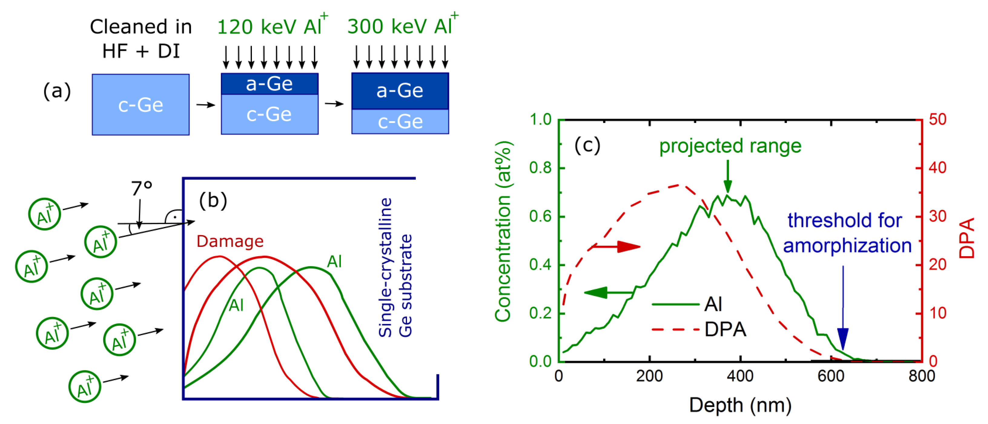
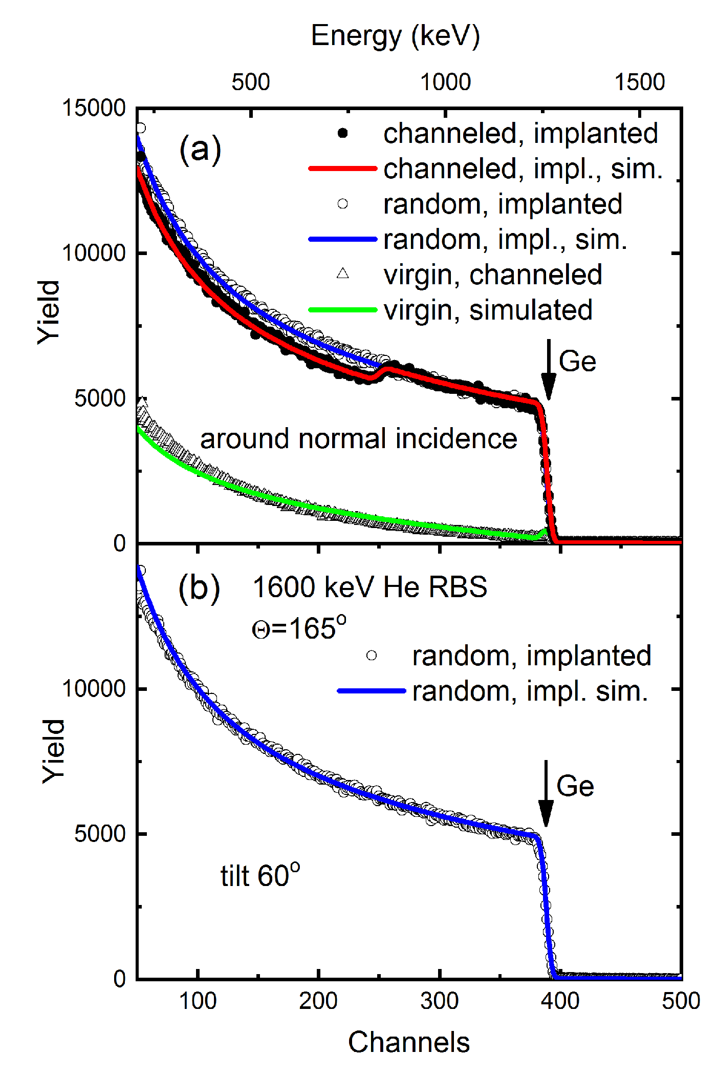
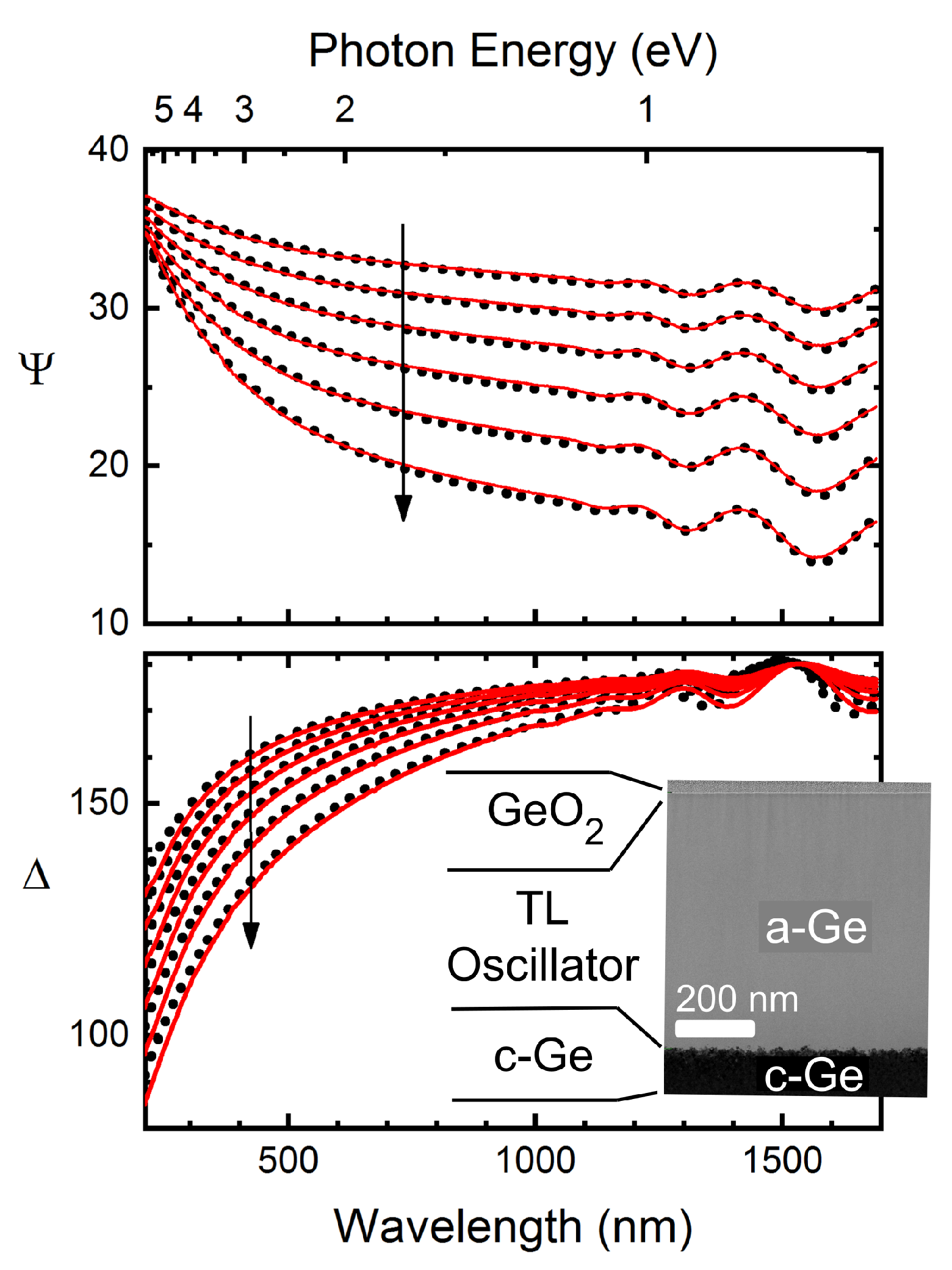
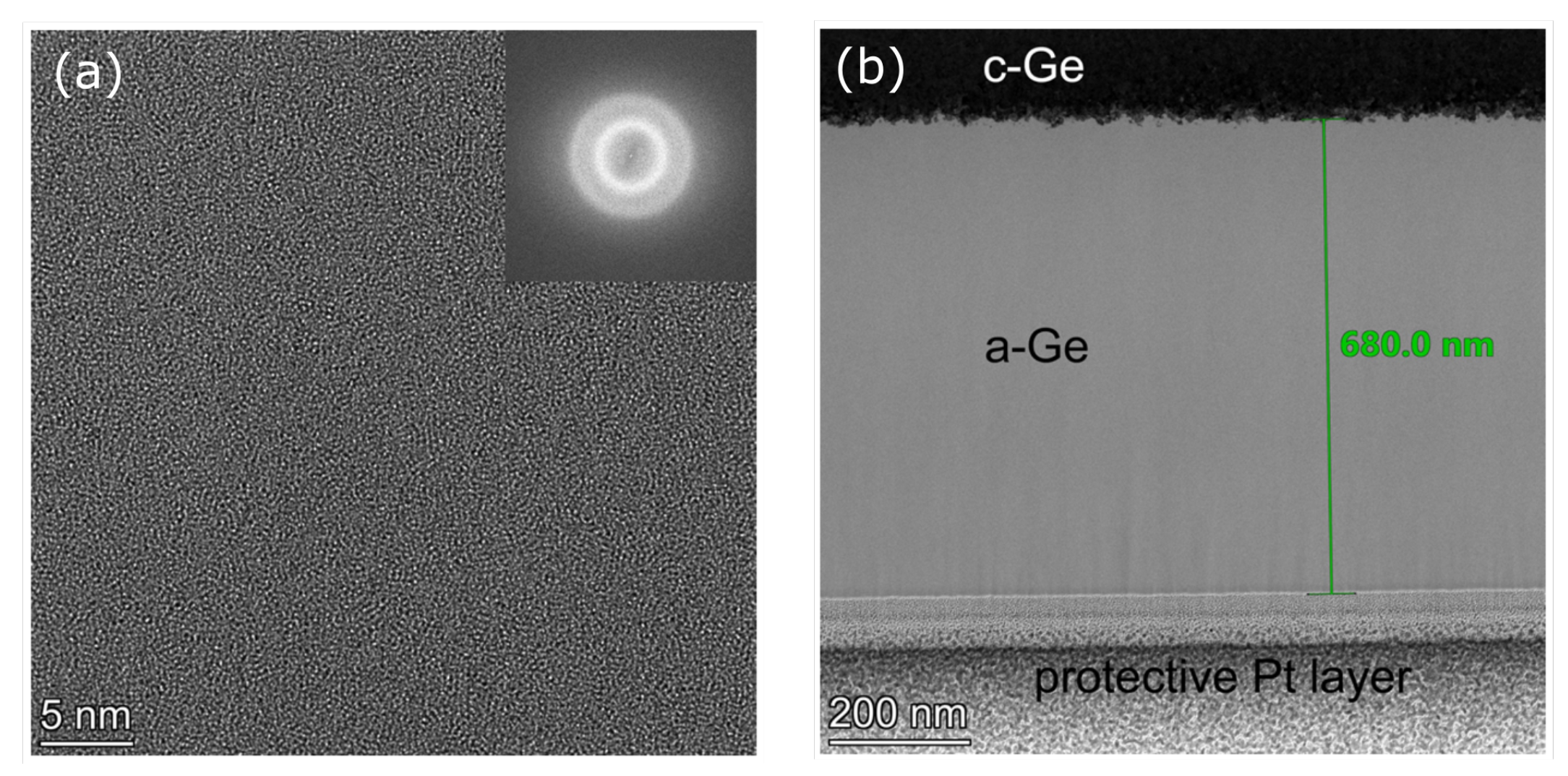
2. Experimental Details

A Ge wafer from Umicore (orientation of (100), resistivity of approx. 0.4 Ω cm, CAS Nr. 7440-56-4) was cleaned in diluted HF (CAS Nr. 7664-39-3) and rinsed in deionized (DI) water. After cutting it into small rectangular pieces, the samples were rinsed again in DI and dried in N gas. To produce a homogeneous amorphous layer from the surface to the buried crystalline-amorphous interface the amorphized layer was created by two step amorphization via ion implantation at room temperature (first step 120-keV Al + (CAS Nr. 7429-90-5) at a fluence of 1 × 10 16 atoms/cm 2 ; second step: 300-keV Al + 1 × 10 16 atoms/cm 2 ) using a heavy-ion cascade implanter (Figure 1a). To avoid the channeling effect during implantation, the sample was tilted by 7 with respect to the ion beam (Figure 1b). Although after the first implantation the Al ions may partially channelled even at tilt 7 [21], the amorphous layer formed by the first ion implantation ensured that the Al ions in the second ion implantation step couldn’t practically get channelled in the sample. The reason for selecting a relatively light mass projectile (Al) was to avoid void formation in case of implantation of heavy mass ions [22].
The damage level caused by ion implantation can be characterised by the displacements per atoms (DPA), i.e., the number of times that an atom is displaced for a given fluence. Figure 1c shows the Al and DPA distribution determined by the simulation software of Stopping and Range of Ions in Matter (SRIM) [23]. SRIM calculates the number of displacements per one implanted ion and per unit depth as a function of depth in the irradiated sample. Considering the implanted fluence (the number of implanted ions per unit area), the value of DPA can be determined for the applied fluence. At depths where the calculated DPA reaches the threshold value (0.3 DPA in our case [24]), the target is supposed to turn to an amorphous phase from crystalline. In our case the DPA value exceeds the threshold from the sample surface down to a depth of 630 nm. Therefore, based on the SRIM simulations, we suppose the position of the a-Ge/c-Ge interface to be at the depth of 630 nm.
The RBS analysis was performed in a scattering chamber equipped with a two-axis goniometer connected to the 5-MV Van de Graaff electrostatic accelerator of the Wigner Research Centre for Physics. The 1.6-MeV He + (CAS Nr. 7440-59-7) analyzing ion beam was collimated with two sets of four-sector slits to the spot size of 0.5 mm by 0.5 mm, while the beam divergence was kept below 0.05 . The beam current was measured by a transmission Faraday cup [25]. The backscattered He + ions were detected using an ORTEC surface barrier detector. The energy resolution of the detection system was 12 keV. The spectra were recorded in Cornell geometry at a scattering angle of 165 for two different sample tilt angles of 7 and 60 . For quantitative compositional analysis both the axial and planar channeling effects of the He + projectiles in the c-Ge substrate were avoided. The measured data were evaluated with the RBX spectrum simulation code [26].
For ex situ ellipsometric characterization a Woollam M-2000DI rotating compensator spectroscopic ellipsometer was used in the wavelength range of 210–1690 nm. The sample for the XTEM investigation was prepared by focused ion beam thinning method. The XTEM investigation was carried out using a Cs-corrected (S)TEM Themis type electron microscope with an operation voltage of 200 keV.

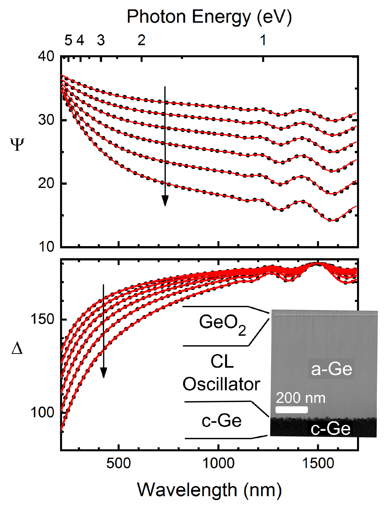
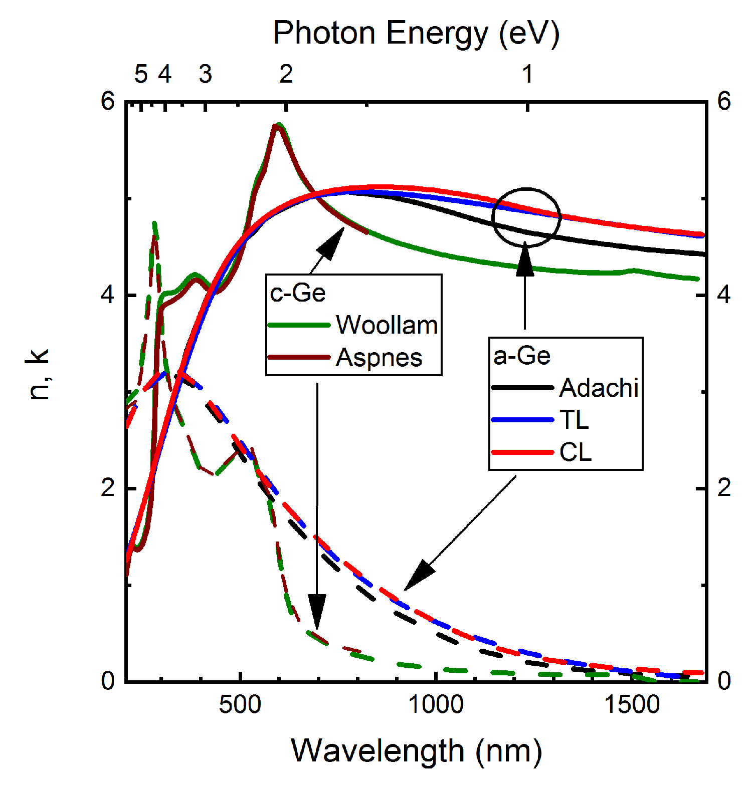
3. Results and Discussion

RBS/C measurements were performed for the analysis of the amorphized Ge layer. To simulate the channeled and random RBS spectra an ia-Ge layer with a thickness of 2.9 × 10 18 ± 1.5 × 10 17 Ge/cm 2 (i.e., 659 ± 33 nm using the density of 4.4 × 10 22 at/cm 3 and the 5% uncertainty of He stopping in Ge) was used. The amorphous Ge layer was formed on top of the c-Ge substrate. The recorded and generated ion beam analytical spectra are displayed in Figure 2. To simulate the dechanneling yield, a lattice strain was taken into account around the range of Al ions. The thickness of the ia-Ge layer agrees with the SRIM simulation within the experimental uncertainty of RBS. The RBS results reveal that the damaged layer is fully amorphized, because the leading edges of the recorded channeled and random spectra coincide.
The agreement between the implanted ion distributions determined by SRIM and RBS is usually much better, because SRIM and RBS use the same stopping powers. Here, besides the Al stopping power, the thickness of the damaged layer also depends on the threshold of amorphization, and therefore the uncertainty of the position of the crystalline-amorphous interface at the damage tail region is larger than that for the ion projected range (see Figure 1a).
The spectra obtained from the multiple-angle-of-incidence spectroellipsometric measurements were evaluated using a two-layer optical model. The evaluation was performed using the WVASE32 software [27]. The generated ellipsometric spectra were fitted on the measured ones using a regression algorithm. The measure of the fit quality is the mean square error (MSE) defined by the following equation [8]:
MSE = 1 2 N M i = 1 n Ψ i m o d Ψ i e x p σ Ψ i e x p 2 + Δ i m o d Δ i e x p σ Δ i e x p 2 ,
where N denotes the number of measured ( Ψ i e x p , Δ i e x p ) data pairs, M is the number of fit parameters, Ψ i m o d and Δ i m o d are the (optical model based) calculated ellipsometric angles at the photon energy E i , whereas Ψ i e x p and Δ i e x p are the measured ellipsometric angles at the photon energy of E i . The σ Ψ , i e x p and σ Δ , i e x p values are the random experimental errors. The unknown parameters are allowed to change until the minimum of MSE is obtained. In order to avoid the local minimum in the regression algorithm, a global search procedure has been applied.
The measured and fitted spectra, as well as the corresponding two-layer optical model are shown in Figure 3. The full-size version of the XTEM image is shown in Figure 4. We determined the optical properties of the native GeO 2 layer from a spectroellipsometric measurement on a 5 nm thick GeO 2 layer deposited by chemical vapor deposition on single crystalline Si. The thickness of the surface oxide layer was found to be less than 2 nm using the two different optical models described below. Using a stoichiometric oxide layer, neglecting a possible nanoscale roughness and the interface between the oxide and the amorphous layer is the usual simplification of the surface structure applied in ellipsometry. The small thickness reveals a high surface quality a-Ge layer, from which we can assume a negligible systematic error caused by the modeling of the a-Ge surface.
First, the TL dispersion relation [21] was applied for the description of the complex dielectric function of the ia-Ge layer (Figure 3). Note that the atomic ratio of the implanted Al is 0.3 percent assuming a homogeneous distribution, and not higher than 1 percent for the peak Al concentration. Therefore, no optical effect from a separate metallic phase has to be assumed. The dielectric function of the c-Ge substrate was from Ref. [15] (also included in the materials library of the WVASE32 software [28]). The thicknesses of the layers and the parameters of the TL model were fitted as free variables. The evaluation yielded a value of 23.2 for the MSE.
In the TL expression the imaginary part of the dielectric function is given as the product of the Tauc law and the Lorentz oscillator function in order to obtain appropriate near-gap and above-gap optical responses, respectively. The Tauc law formula was derived on the assumption of parabolic bands and a constant momentum matrix element. The real part of the dielectric function is obtained by applying the Kramers–Kronig transformation. The Tauc-Lorentz oscillator allows for a band gap, i.e., a non-absorbing region below the band gap energy E g and describes the onset of absorption close to the band gap.
The resulting fitted parameters of both optical models for the ia-Ge sample are shown in Table 1. Only five free parameters describe the dielectric function of the ia-Ge layer: the amplitude, the resonant energy (or peak transition energy), the broadening term, the bandgap energy and the offset parameter of the Kramers-Kronig transformation.
The high MSE value (23.2) and the imperfect agreement between the measured and generated SE spectra of the TL model in certain wavelength regions (see the wavelength range above 1300 nm for Δ ) motivated us to perform a new evaluation using the CL dispersion relation for the description of the complex dielectric function of the ia-Ge layer.
The two-layer optical model as well as the measured and fitted spectra using the CL dispersion relation is shown in Figure 5. Here, the thickness of the layers and the parameters of the CL model were fitted as free variables. The free parameters describe the thicknesses of the oxide and the ia-Ge layer, as well as the dielectric function by adding three more parameters to the TL oscillator model: the transition energy between the absorption onset and the Lorentz oscillator ( E p ), the demarcation energy between the Urbach tail transitions and the band-to-band transitions ( E t ), and the Urbach tail parameter ( E u )—see Table 1. Note that the MSE value is much better (9.7) than that of the TL model (23.2—also shown in Table 1) and the difference between the measured and generated SE spectra indicate a good agreement (see for example the improvement for Δ in the above-mentioned range of wavelengths larger than 1300 nm). When fitting on the Ψ and Δ ellipsometric angles, an MSE below 10 is usually acceptable [8]. It may be possible to improve when adding more oscillators to the model, but at the cost of increasing parameter correlations and uncertainties. The results show that the simple one-oscillator CL model fits the data perfectly in the wavelength range below ≈4.5 eV.
The n and k values obtained by the evaluation of the measured SE spectra using the CL and TL models are shown in Figure 6. For comparison, the data of c-Ge and evaporated a-Ge are also presented. There is only a small difference between the TL and CL dispersions. Moreover, the discrepancy between the ia-Ge and the evaporated a-Ge was found to be smaller than for amorphous silicon [29].
The thickness values of the ia-Ge layer determined by SE and the theoretical thickness of damaged region estimated by SRIM agree with the thickness value determined by RBS/channeling technique within the experimental uncertainty of RBS. However, SE gives a somewhat larger thickness value compared to RBS; probably SE is more sensitive to damage than the RBS/channeling technique.
The images obtained by XTEM investigation are shown in the insets of Figure 3 and Figure 5. The HRTEM image shown in Figure 4 and its fast Fourier transrom (FFT) obtained by XTEM method (as well as the insets of Figure 3 and Figure 5) show a completely amorphized germanium layer. This result justifies the appropriate choice of Al for the ion implantation, because a high quality, void-free, dense and completely amorphous Ge layer was formed. The density of the a-Ge layer found in our study is even higher than that was reported in Ref. [15]. This result is also reflected in our n and k values which are slightly higher than that shown in Ref. [15], especially at higher wavelengths.

4. Conclusions

The complex dielectric function of ia-Ge produced by ion implantation was determined by SE in the wavelength range from 210 to 1690 nm. It was found that the CL dispersion relation is more appropriate for the evaluation of the SE measurements on ia-Ge than the TL model. The thickness values yielded by the TL and by the CL type SE evaluations are close to the thickness value deduced from the ion beam analytical measurements and XTEM investigation. The obtained dielectric function spectra are in good agreement with those measured by Adachi et al. [15], providing a solid and reliable basis of further in situ investigations of amorphization processes in Ge.

Author Contributions

T.L. performed the ellipsometry measurements, the evaluations and wrote the manuscript; A.N. performed the ion irradiation; E.S., Z.Z., and E.K. measured and evaluated the RBS/C spectra; Z.F. and L.I. measured by electron microscopy; P.P. wrote the manuscript and coordinated the work; M.F. coordinated the work. All authors have read and agreed to the published version of the manuscript.

Funding

This research was funded by the National Development Agency grant OTKA K131515, VEKOP- 2.3.3-15-2016-00002 and grant NKFIH-OTKA 129009.

Conflicts of Interest

The authors declare no conflict of interest. The funders had no role in the design of the study; in the collection, analyses, or interpretation of data; in the writing of the manuscript, or in the decision to publish the results.

Abbreviations

The following abbreviations are used in this manuscript:
CL modelCody-Lorentz model
DIDeionized Water
DPADisplacements per Atoms
FFTFast Fourier Transform
MSEMean Square Error
RBSRutherford Backscattering Spectrometry
SESpectroscopic Ellipsometry
SRIMStopping and Range of Atoms in Matter
TL modelTauc-Lorentz model
XTEMCross-sectional Transmission Electron Microscopy

References

  1. Lohner, T.; Kalas, B.; Petrik, P.; Zolnai, Z.; Serényi, M.; Sáfrán, G. Refractive Index Variation of Magnetron-Sputtered a-Si1-xGex by ’One-Sample Concept’ Combinatory. Appl. Sci. 2018, 8, 826. [Google Scholar] [CrossRef] [Green Version]
  2. Kalas, B.; Zolnai, Z.; Safran, G.; Serenyi, M.; Agocs, E.; Lohner, T.; Nemeth, A.; Fried, M.; Petrik, P. Micro-combinatorial sampling of the optical properties of hydrogenated amorphous Si1-xGex for the entire range of compositions towards a database for optoelectronics. Sci. Rep. 2020. submitted. [Google Scholar]
  3. Cosentino, S.; Miritello, M.; Crupi, I.; Nicotra, G.; Simone, F.; Spinella, C.; Terrasi, A.; Mirabella, S. Room-temperature efficient light detection by amorphous Ge quantum wells. Nanoscale Res. Lett. 2013, 8, 128. [Google Scholar] [CrossRef] [PubMed] [Green Version]
  4. Leem, J.W.; Yu, J.S. Design and fabrication of amorphous germanium thin film-based single-material distributed Bragg reflectors operating near 2.2 μm for long wavelength applications. JOSA B 2013, 30, 838–842. [Google Scholar] [CrossRef]
  5. Colace, L.; Balbi, M.; Masini, G.; Assanto, G.; Luan, H.C.; Kimerling, L.C. Ge on Si p-i-n photodiodes operating at 10Gbit/s. Appl. Phys. Lett. 2006, 88, 101111. [Google Scholar] [CrossRef]
  6. Carletti, L.; Sinobad, M.; Ma, P.; Yu, Y.; Allioux, D.; Orobtchouk, R.; Brun, M.; Ortiz, S.; Labeye, P.; Hartmann, J.M.; et al. Mid-infrared nonlinear optical response of Si-Ge waveguides with ultra-short optical pulses. Opt. Express 2015, 23, 32202. [Google Scholar] [CrossRef] [Green Version]
  7. Bean, J. Silicon-based semiconductor heterostructures: Column IV bandgap engineering. Proc. IEEE 1992, 80, 571–587. [Google Scholar] [CrossRef] [Green Version]
  8. Fujiwara, H. Spectroscopic Ellipsometry: Principles and Applications; John Wiley & Sons Ltd.: Chichester, UK, 2007. [Google Scholar]
  9. Castriota, M.; Politano, G.G.; Vena, C.; De Santo, M.P.; Desiderio, G.; Davoli, M.; Cazzanelli, E.; Versace, C. Variable Angle Spectroscopic Ellipsometry investigation of CVD-grown monolayer graphene. Appl. Surf. Sci. 2019, 467–468, 213–220. [Google Scholar] [CrossRef]
  10. Nemeth, A.; Kozma, P.; Hülber, T.; Kurunczi, S.; Horvath, R.; Petrik, P.; Muskotál, A.; Vonderviszt, F.; Hos, C.; Fried, M.; et al. In Situ Spectroscopic Ellipsometry Study of Protein Immobilization on Different Substrates Using Liquid Cells. Sens. Lett. 2010, 8, 730–735. [Google Scholar] [CrossRef]
  11. Fricke, L.; Böntgen, T.; Lorbeer, J.; Bundesmann, C.; Schmidt-Grund, R.; Grundmann, M. An extended Drude model for the in-situ spectroscopic ellipsometry analysis of ZnO thin layers and surface modifications. Thin Solid Films 2014, 571, 437–441. [Google Scholar] [CrossRef]
  12. Al-Mahasneh, A.; Al Attar, H.; Shahin, I. Spectroscopic ellipsometry of single and multilayer amorphous germanium/aluminum thin film systems. Opt. Commun. 2003, 220, 129–135. [Google Scholar] [CrossRef]
  13. Beaglehole, D.; Zavetova, M. The fundamental absorption of amorphous Ge, Si and GeSi alloys. J. Non-Cryst. Solids 1970, 4, 272–278. [Google Scholar] [CrossRef]
  14. Rafla-Yuan, H.; Rancourt, J.; Cumbo, M. Ellipsometric study of thermally evaporated germanium thin film. Appl. Opt. 1997, 36, 6360–6363. [Google Scholar] [CrossRef] [PubMed]
  15. Adachi, S. Optical Constants of Crystalline and Amorphous Semiconductors: Numerical Data and Graphical Information; Springer: New York, NY, USA, 1999. [Google Scholar]
  16. Wei, P.; Xu, Y.; Nagata, S.; Narumi, K.; Naramoto, H. Structure and optical properties of germanium implanted with carbon ions. Nucl. Instrum. Methods Phys. Res. Sect. B: Beam Interact. Mater. Atoms 2003, 206, 233–236. [Google Scholar] [CrossRef]
  17. Aspnes, D.; Studna, A. An investigation of ion-bombarded and annealed 111 surfaces of Ge by spectroscopic ellipsometry. Surf. Sci. 1980, 96, 294–306. [Google Scholar] [CrossRef]
  18. Dekker, J.; Zandvliet, H.; van Silfhout, A. Low energy ion bombardment on c-Ge surfaces. Vacuum 1990, 41, 1690–1691. [Google Scholar] [CrossRef] [Green Version]
  19. Jellison, G.E.; Modine, F.A. Erratum: “Parameterization of the optical functions of amorphous materials in the interband region” [Appl. Phys. Lett. 69, 371 (1996)]. Appl. Phys. Lett. 1996, 69, 2137. [Google Scholar] [CrossRef]
  20. Ferlauto, A.S.; Ferreira, G.M.; Pearce, J.M.; Wronski, C.R.; Collins, R.W.; Deng, X.; Ganguly, G. Analytical model for the optical functions of amorphous semiconductors from the near-infrared to ultraviolet: Applications in thin film photovoltaics. J. Appl. Phys. 2002, 92, 2424–2436. [Google Scholar] [CrossRef] [Green Version]
  21. Nordlund, K.; Djurabekova, F.; Hobler, G. Large fraction of crystal directions leads to ion channeling. Phys. Rev. B 2016, 94, 214109. [Google Scholar] [CrossRef] [Green Version]
  22. Kaiser, R.; Koffel, S.; Pichler, P.; Bauer, A.; Amon, B.; Claverie, A.; Benassayag, G.; Scheiblin, P.; Frey, L.; Ryssel, H. Honeycomb voids due to ion implantation in germanium. Thin Solid Films 2010, 518, 2323–2325. [Google Scholar] [CrossRef]
  23. Ziegler, J.F.; Ziegler, M.; Biersack, J. SRIM – The stopping and range of ions in matter (2010). Nucl. Instrum. Methods Phys. Res. Sect. B: Beam Interact. Mater. Atoms 2010, 268, 1818–1823. [Google Scholar] [CrossRef] [Green Version]
  24. Birtcher, R. Energy dependence of amorphization of Ge by Kr ions. MRS Online Proc. Libr. Arch. 1993, 279, 129–134. [Google Scholar] [CrossRef] [Green Version]
  25. Pászti, F.; Manuaba, A.; Hajdu, C.; Melo, A.; Da Silva, M. Current measurement on MeV energy ion beams. Nucl. Instrum. Methods Phys. Res. B 1990, 47, 187–192. [Google Scholar] [CrossRef]
  26. Kótai, E. Computer methods for analysis and simulation of RBS and ERDA spectra. Nucl. Inst. Methods Phys. Res. B 1994, 85, 588–596. [Google Scholar] [CrossRef]
  27. Woollam Co. Inc. Available online: http://www.jawoollam.com (accessed on 15 April 2020).
  28. (Ge Tabulated from UNL (Multiple Data Sets Fit)—Data in the Woollam Software Library). Available online: /WVASE32new/mat/Ge.mat (accessed on 13 April 2020).
  29. Fried, M.; Lohner, T.; Aarnink, W.; Hanekamp, L.; Van Silfhout, A. Determination of complex dielectric functions of ion implanted and implanted-annealed amorphous silicon by spectroscopic ellipsometry. J. Appl. Phys. 1992, 71, 5260–5262. [Google Scholar] [CrossRef] [Green Version]
  30. Aspnes, D.E.; Studna, A.A. Dielectric functions and optical parameters of Si, Ge, GaP, GaAs, GaSb, InP, InAs, and InSb from 1.5 to 6.0 eV. Phys. Rev. B 1983, 27, 985–1009. [Google Scholar] [CrossRef]
Sample Availability: The dielectric function data determined for the amorphous Ge layer created by implantation of Al ions can be downloaded from https://seafile.it.energia.mta.hu/f/32291c1f099541ba855d/?dl=1.
Figure 1. (a) Process steps of sample preparation. From left to right: cleaning in HF and DI; implantation of 120 keV Al ions; finally, implantation of 300 keV Al ions. (b) Schematic drawing of the dual-energy ion implantation showing the damage (red curves) and Al (green curves) profiles. The blue box shows the c-Ge substrate into which Al ions (green circles at the left-hand side) are implanted at well-defined energies and tilt angles of 7 in order to avoid the channeling of the ions. (c) Simulated Al concentration and Ge damage profile caused by the implantation of Al into Ge using an energy of 300 keV and a fluence of 1 × 10 16 Al/cm 2 . The calculation was performed by the SRIM software. The threshold for the amorphization level of 0.3 DPA corresponds to a damaged layer thickness of 630 nm. Note, that the peak Al concentration is less than 0.7 at%.
Coatings 10 00480 g001
Figure 2. Comparison of measured (symbols) and simulated (lines) RBS spectra of the Al-implanted Ge sample (a) in channeling conditions around normal incidence. The channeling spectrum of virgin Ge is also shown (b) in random conditions at the sample tilt of 60 .
Coatings 10 00480 g002
Figure 3. Measured (solid lines) and generated (dotted lines) ellipsometric Ψ and Δ spectra for the Al-implanted Ge sample. The two-layer optical model and the corresponding XTEM micrograph is shown in the inset. The fitted thicknesses of the surface oxide (GeO 2 ) and a-Ge (TL oscillator) layers are 1.61 ± 0.03 and 679.4 ± 0.3 nm, respectively. Note that the top part of the XTEM image is the glue used for the sample preparation. The 1.6-nm oxide itself is not visible. The arrows show the direction of increasing angles of incidence from 53 in steps of 3 .
Coatings 10 00480 g003
Figure 4. (a) HRTEM image and its fast Fourier transform (FFT) showing a completely amorphized Ge layer. (b) Image obtained by XTEM method showing a completely amorphized germanium layer of 680 nm thickness on c-Ge.
Coatings 10 00480 g004
Figure 5. Measured and generated ellipsometric Ψ and Δ spectra for the Al-implanted Ge sample. The two-layer optical model and the corresponding XTEM micrograph revealing a completely amorphized layer with a thickness of 681 nm is shown in the inset. The fitted thicknesses of the surface oxide (GeO 2 ) and the amorphous Ge (CL oscillator) layers are 1.74 ± 0.01 and 678.9 ± 0.1 nm, respectively. Note that the top part of the XTEM image is the glue used for the sample preparation. The 1.7-nm oxide itself is not visible. The arrows show the direction of increasing angles of incidence from 53 in steps of 3 .
Coatings 10 00480 g005
Figure 6. n (solid lines) and k (dashed lines) spectra given by the evaluation of the measured SE data using the CL and TL dispersions. For comparison, the data of c-Ge [28,30] and evaporated a-Ge [15] (Adachi) are also presented.
Coatings 10 00480 g006
Table 1. Fitted parameters of both parametric models for the ia-Ge layer.
ParameterTL ModelCL Model
Oxide thickness (nm)1.61 ± 0.031.74 ± 0.01
a-Ge layer thickness (nm)679.4 ± 0.3678.9 ± 0.1
Amplitude142.4 ± 0.492.7 ± 0.2
Energy position (eV)3.042 ± 0.0043.355 ± 0.002
Broadening (eV)3.95 ± 0.014.08 ± 0.01
Band gap (eV)0.622 ± 0.0010.689 ± 0.002
Offset0.14 ± 0.020.62 ± 0.01
Ep (eV) 0.561 ± 0.004
Et (eV) 0.39 ± 0.05
Eu (eV) 0.189 ± 0.001
Mean Square Error23.29.7

