


Abstract
We numerically and experimentally investigate the phononic loss for superconducting resonators fabricated on a piezoelectric substrate. With the help of finite element method simulations, we calculate the energy loss due to electromechanical conversion into bulk and surface acoustic waves. This sets an upper limit for the resonator internal quality factor Qi. To validate the simulation, we fabricate quarter wavelength coplanar waveguide resonators on GaAs and measure Qi as function of frequency, power and temperature. We observe a linear increase of Qi with frequency, as predicted by the simulations for a constant electromechanical coupling. Additionally, Qi shows a weak power dependence and a negligible temperature dependence around 10 mK, excluding two level systems and non-equilibrium quasiparticles as the main source of losses at that temperature.
Export citation and abstract BibTeX RIS

Original content from this work may be used under the terms of the Creative Commons Attribution 4.0 licence. Any further distribution of this work must maintain attribution to the author(s) and the title of the work, journal citation and DOI.
1. Introduction
Superconducting coplanar waveguide (CPW) resonators in the microwave regime have been extensively used in circuit quantum electrodynamics (circuit-QED) because of their high performance (e.g. internal quality factors (Qi) can exceed 1 million [1]). Well established and consistent fabrication techniques lead to devices that match its designed parameters, allowing for the implementation of circuits with many multiplexed resonators [2]. Moreover, such resonators have a high spatial confinement of the electric field that enhances the zero point fluctuations, making the resonators suitable for strong coupling with other quantum systems [3, 4]. Nevertheless, energy losses still exist due to energy escaping to the environment.
Recently, a large effort has been made to understand and reduce the causes of energy loss in superconducting circuits. Primarily, the investigation has focussed on geometry [5], substrate and superconductor materials [6, 7], as well as fabrication methods [8, 9]. Additionally, other efforts have explored how wire bonding [10] and shielding of the sample box [11] affect the performance of the resonators. One finds the same aforementioned factors responsible for the energy loss of other devices in circuit QED, such as quantum bits (qubits) [12]. This is not surprizing since the resonators are fabricated with the same materials, following the same lithographic process, are measured in the same environment and with the same electromagnetic excitation.
Here, we find that despite well established processing and measurement techniques, CPW resonators fabricated on a piezoelectric substrate are not limited by any of the above factors. This type of substrate has recently been used for building devices that combine circuit QED with mechanical excitations at quantum level [13–18]. From a broader point of view, superconducting CPW resonators enable studies of semiconductor qubits realized on piezoelectric substrate [19, 20] and even to couple them to superconducting qubits [21]. In these hybrid systems, resonators typically have a Qi 100 times lower than in comparable devices on low dielectric loss and non-piezoelectric substrates, such as silicon or sapphire. Such observations strongly suggest that piezoelectricity introduces an additional loss channel due to its electromechanical coupling.
In this work, we investigate the mechanical loss channel of superconducting CPW resonators fabricated on gallium arsenide (GaAs). Firstly, we numerically study the dynamics of the mechanical wave generation. Using finite element method (FEM) simulations we show that an oscillating electric field in the resonator leads to the generation of bulk and surface acoustic waves (BAWs and SAWs). A numerical evaluation of the energy loss due to the electromechanical conversion is used to calculate the loss rate and the internal quality factor of the resonators. The simulations predict a linear increase of Qi with the resonator frequency.
Secondly, we measure the performance of CPW resonators, fabricated on GaAs substrates. We find that the measured quality factors agree well with the numerical simulation, following the predicted linear increase as a function of frequency.
Finally, we observe a weak dependence of Qi as a function of power and sample temperature. Using a two-level-systems (TLSs) loss model [22] for fitting the response of Qi as a function of input power, we find that the TLS loss is comparable to those on non-piezoelectric substrates. Furthermore, we measure the temperature dependence of Qi and the resonance frequency fr. Then, from these fits, we determine the loss rate to quasiparticles (QPs). We find both TLSs and QPs contribute significantly less to losses than the electromechanical conversion.
2. Method
2.1. Design and fabrication
The measurements are performed on three different designs of quarter wavelength ( ) CPW resonators. The first geometry (figure 1(a)), labelled vertical 1 and vertical 2, consists of two nominally identical chips, each containing six resonators with different frequencies. The second geometry (figure 1(b)), labelled horizontal 1 and horizontal 2, also consists of two nominally identical chip with eight different resonators. However, these chips have a perpendicular orientation with respect to the vertical samples (the crystallography directions are shown in figure 1). All resonators are multiplexed in a notch geometry with inductive coupling to a feedline. Their length is chosen such that the fundamental mode of each resonator lies in the 4–8 GHz band. The last design, sample harmonics, consists of a single long multimode-resonator, with the fundamental resonance frequency at 450 MHz, and a capacitive coupling to the feedline. The main features of all devices are summarized in table 1.
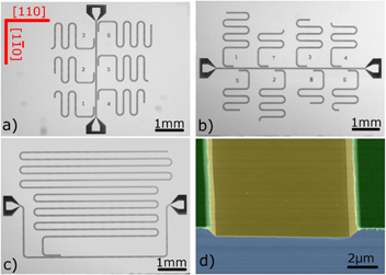
Figure 1. The measured devices and a cross-cut of the CPW structure. (a) Optical microscope image of a 5 × 7 mm2 chip of the type vertical: the brighter part is the 150 nm aluminium film deposited on the darker GaAs substrate. The crystallographic direction of the GaAs lattice are highlighted in red. (b) Optical microscope image of a horizontal chip. (c) Optical microscope image of a harmonics chip. (d) False colour scanning electron microscope image of the gap (GaAs, yellow) between the ground plane and the centre conductor (aluminium, both green). In the gap area, the GaAs substrate is etched to a depth of about 1–2 μm, creating trenches that slightly increase the resonator performance.
Download figure:
Standard image High-resolution imageTable 1. The five measured devices and their most important features are summarized. The corresponding chips are shown in figure 1. All chips are made of aluminium on gallium arsenide. The orientation refers to the direction of the longest straight segment in the meandering part of the resonators. In the last column the main coupling mechanism to the feedline is reported.
| Sample | Figure | Orientation | Trench (μm) | Coupling |
|---|---|---|---|---|
| Vertical 1 | 1(a) | [110] | 1.5 ± 0.3 | Inductive |
| Vertical 2 | 1(a) | [110] | 1.5 ± 0.3 | Inductive |
| Horizontal 1 | 1(b) | ![$\left[1\overline{1}0\right]$](https://content.cld.iop.org/journals/1367-2630/22/5/053027/revision2/njpab8044ieqn2.gif) | 0.6 ± 0.2 | Inductive |
| Horizontal 2 | 1(b) | ![$\left[1\overline{1}0\right]$](https://content.cld.iop.org/journals/1367-2630/22/5/053027/revision2/njpab8044ieqn3.gif) | 0.8 ± 0.2 | Inductive |
| Harmonics | 1(c) | ![$\left[1\overline{1}0\right]$](https://content.cld.iop.org/journals/1367-2630/22/5/053027/revision2/njpab8044ieqn4.gif) | 0.8 ± 0.2 | Capacitive |
The resonators are fabricated with a common lithography process on the (100) polished surface of a commercial epi-ready 2 inch GaAs wafer. The wafers come individually packaged in an air tight plastic package. Within the cleanroom, the package is opened and immediately placed in the load lock chamber of an electron-beam evaporator (Plassys MEB550S) and pumped to a pressure of 10−7mbar. While pumping the wafer is heated to 300 °C and kept at this temperature for 10 min. The wafer cools down while the system reaches its base pressure of 4 × 10⁻⁸mbar, which takes 10 h. A layer of 150 nm of 99.999% (5 N) pure aluminium is evaporated while the wafer rotates around its axis to increase the film homogeneity. The aluminium surface is oxidized after the evaporation by 10 mbar static pressure of 99.99% (4 N) pure oxygen in the chamber. After removing the metalized wafer from the Plassys MEB550S, a 1.3 μm thin AZ1512 resist layer is spun on the wafer and baked at 112 °C. The resist is then patterned with a laser writer (Heidelberg DWL2000). Prior to development, an additional thick protective layer of the same resist is spun on the back side of the wafer and baked in an oven at 110 °C for 2 min. The extra resist prevents the production of gallium arsenide dust due to etching of the back side of the wafer. The patterned resist is then developed with an AZ dev:H2O 1:1 solution followed by a mild ashing in an oxygen plasma. The design is then wet etched with the commercially available Transene type A aluminium etchant. When the exposed aluminium is etched away, the unprotected GaAs surface beneath is rapidly etched by the acid solution, as shown in figure 1(d), creating trenches of 1–2 μm under the gaps in the resonator electrodes.
2.2. Experimental setup
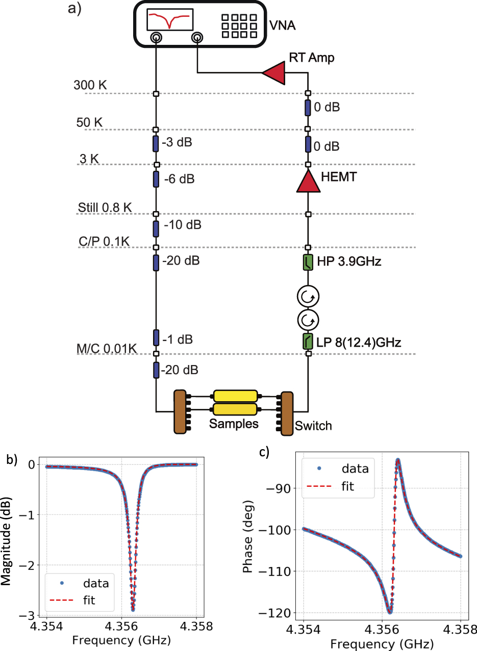
The chips are wire-bonded in an oxygen-free copper sample-box with aluminium wire. The sample-box is thermally and mechanically anchored at the mixing chamber stage of a Bluefors LD250 dilution refrigerator and cooled to a base temperature of 10 mK (see figure 2(a)). Two different setups are used to measure the resonators. For samples vertical 1 and vertical 2 a narrow-band 4–8 GHz HEMT amplifier is used. Samples horizontal 1, horizontal 2 and harmonics are measured with a wider band 3–12 GHz HEMT amplifier and wider circulators. After an additional stage of room temperature (RT) amplification, their transmission spectra are measured with a vector network analyzer (VNA).
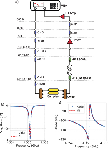
Figure 2. (a) Cryogenic and room temperature setup used in the resonator measurement. The presence of microwave switches at the mixing chamber stage allows the measurement of multiple chips during the same cooldown. (b) Magnitude and (c) phase as function of frequency of the transmitted signal measured for one of the resonators of the sample vertical 1 (blue dots). Qi is extracted with a global fit in quadrature space (red dashed line).
Download figure:
Standard image High-resolution imageThe resonators Qi, together with the coupling quality factor Qc and the resonance frequency, are extracted using the circle fit routine [23]. The measured and fitted amplitude and phase of one resonator transmission spectrum (sample vertical 1) are shown in figure 2. The routine globally fits the imaginary and real part of the resonator spectrum.
2.3. Numerical modelling
An experimental study of the mechanical waves generated by the resonators is difficult. A relatively large level of excitation, corresponding to 109 photons in the resonators or an electrical energy Eint ≈ 10−15 J (see equation (3)), produces a small potential between the superconductor electrodes  of the order of 10−1 V, where
  0 and r are the vacuum and relative dielectric constant respectively, d is the distance between the resonator electrodes, V0 = d2l is the volume where the electric field has the largest intensity and l the resonator length. This potential generates displacements that do not exceed
 ![$s={d}_{\mathrm{max}}\left[\frac{{e}_{ijk}}{{c}_{ijkl}}\right]E\approx 1{0}^{-13}$](https://content.cld.iop.org/journals/1367-2630/22/5/053027/revision2/njpab8044ieqn6.gif) m, where eijk is the piezoelectric tensor, cijkl the elasticity tensor and E is the electric field. Although there are techniques capable of detecting such a small displacement [24, 25], they are very hard to use at 10 mK, over a large area and within a closed sample-box.
m, where eijk is the piezoelectric tensor, cijkl the elasticity tensor and E is the electric field. Although there are techniques capable of detecting such a small displacement [24, 25], they are very hard to use at 10 mK, over a large area and within a closed sample-box.
We would like to remark that the largest average photon number that we are able to excite the cavity is slightly below 109 (see figure 6). Excitation levels with much lower photon number generate waves that cannot be detected with the mentioned methods.
Instead, in order to study and predict the behaviour of the resonators we develop a numerical model of the system. The model is realized using a commercial finite element analysis software (COMSOL Multiphysics, version 5.3a, piezoelectric module, time dependent study). We use this model to calculate the strain tensor sij and the velocity v at each point in a grid that discretizes the substrate, given an electrical excitation as an initial condition. From these quantities, using the COMSOL structural mechanics module [26], it is possible to calculate the mechanical energy released into the substrate:

where ρ is the substrate density and V its volume.
This calculation can be repeated at each time during the evolution of the system, and its time derivative represents the mechanical energy loss rate Lmech. As already mentioned, other sources of energy loss may contribute to the Qi of the resonator, in particular TLS and QP loss rates, denoted LTLS and LQP respectively. The internal Qi value is defined and divided into different terms as:

where additional unknown sources of losses have been taken into account in a residual loss rate Lresidual, and the corresponding quality factor Qresidual. We need to take all of them into account to determine the dominant one.
A full scale three-dimensional (3D) model is intractable on a desktop computer: the full chip is 5 × 7 × 0.35 mm3, and the mechanical wavelength at 6 GHz is about 0.5 μm. A good discretization would require at least 1014 elements, each with the mechanical and the electric degrees of freedom. In order to use a desktop computer we can instead exploit the cubic symmetry of the GaAs elastic tensor, and the tranlational invariance of the CPW resonator. The mechanical displacement produced by the transverse electric magnetic (TEM) mode in the resonator is confined in the transverse plane when the resonators electrodes direction is [110] or [ ]. Thus we can reduce our model to a two dimensional (2D) simulation [27].
Our model geometry consists of a 2D section perpendicular to the CPW resonator and the substrate surface near the electrode (the blue surface in the false colour SEM picture in figure 1(d)). The metallic layer of the electrodes and the vacuum are also included in the simulation.
The maximum element dimension for the mesh is dynamically adapted as a function of the simulation frequency: the wavelength λ of SAWs and BAWs can be calculated from their speed in GaAs for each frequency, and the element mesh size, δx, does not exceed 0.1λ.
The electric potential on the metallic layer is changed periodically following a harmonic oscillation V = V0sin(2πft). The simulation time consists of 10 oscillation periods, and the time discretization δt follows the Courant condition [28], i.e. the numerical speed  is larger than the wave propagation velocity. During this time the mechanical waves generated do not reach the edge of the substrate because the total dimension of the substrate is dynamically adapted to the frequency of the simulation to prevent this possibility.
2.4. Simulation limitations
The five orders of magnitude difference between the phononic and photonic wavelength limits the dimensions of the device (or device portion) that can be simulated. As already mentioned, we cannot simulate the full chip, and not even a single resonator in 3D. In a case where the elastic and the piezoelectric tensor have less symmetry than GaAs, our approach does not work and instead quasi-3D simulations are needed.
The large difference between light and sound speed allows us to simplify the full electromagnetic problem into an electrostatic one. The electrostatic equations are coupled to the mechanical dynamics ones, such that a solution is found for the electrostatic part and updated instantly to the full domain. This is justified since the slow mechanical dynamics behaves as quasi-static compared to the time scale of electromagnetic evolution.
Finally our simulations show that the steady state regime in the energy conversion is reached after a few oscillations. Nevertheless, this is not the real system steady state, because we are ignoring the back scattering at the boundaries of the chip. Unfortunately we cannot take this into account due to the dimensions of the substrate.
3. Simulations results
3.1. Bulk and surface acoustic waves conversion rate
The main result of the simulation is the calculation of the electrical energy converted into mechanical strain energy and kinetic energy. The total mechanical energy is subtracted from the electromagnetic energy stored in the resonator and it leaves the area close to the electrodes as surface and bulk acoustic waves: this is the mechanical part of the loss rate of the resonator.
Figure 3 shows the displacement of the substrate from its rest position six periods after the electric oscillating potential was applied to the electrodes. The larger displacements are due to BAWs that travel inside the substrate. The SAWs generated travel along the surface and the larger deformation is located in and under the metallic layer.
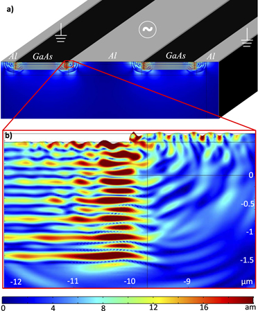
Figure 3. (a) Displacement of the substrate and the metal layer six periods after the 10 GHz electrical oscillation is applied. Following the colour scale, the points of larger displacement from the equilibrium condition are located in the red area, while the blue area represents the points that are at rest position. (b) Zoom in the edge of the electrode [red rectangle in (a)] highlights the piezoelectric conversion of electric field into BAWs generated on the surface propagating inside the substrate, while SAWs travel on the surface. The deformation in the plot has been amplified by 2 × 10⁹ times to make it visible. Additional details regarding the simulation, including the time evolution of the mechanical deformation, are shown in the supplementary material (http://stacks.iop.org/NJP/22/053027/mmedia).
Download figure:
Standard image High-resolution imageBy integrating the mechanical energy density on the substrate domain (see equation (1)), it is possible to estimate the loss rate due to the piezoelectric effect (see figure 4). The dominant loss is due to BAWs, the energy converted to SAWs represents only 2% of the total mechanical energy, and can be estimated by integrating only in a two wavelengths thick superficial layer, excluding the zone right below the CPW gap.

Figure 4. Numerical evaluation of the total mechanical energy density released in the substrate as acoustic waves (SAWs and BAWs), versus the number of oscillations of the electric field at different frequencies. The calculation of Qi takes into account the steady state slope of the electromechanical conversion rates, and it is extracted with a linear fit. The SAWs represents 2% of the total mechanical energy released into the substrate.
Download figure:
Standard image High-resolution imageIt is interesting to notice that the energy lost in an oscillation period decreases with frequency. This is easily understood if we consider that the electromechanical coupling is almost constant in the GHz range: on one hand, the energy converted in mechanical excitation has a constant rate but as the frequency increases the period gets shorter leading to a reduction of total energy lost per period. On the other hand, the electric energy stored in the resonator does not change with frequency. Therefore the Qi, their ratio, increases as a function of frequency.
The expected linear increase of the internal quality factor of a quarter-wavelength CPW resonator as a function of frequency [29] is usually overcome by a corresponding increase in the intrinsic loss tangent.
We simulate the wave generation with and without trenches under the electrodes gap, and calculate the conversion rates for different frequencies. The value of these loss rates is used to estimate the Qmech, and the results are shown in figure 5. From this quantity, we can extract the Qi as shown in equation (2). We find an almost linear increase of the internal Q-factor with respect to frequency.

Figure 5. Internal Q-factor (at 107 photons stored in the resonator) of the resonators fabricated on different samples and the values extracted from the simulations. Each point of sample vertical 1 and 2, horizontal 1 and 2, represents Q-factor at the fundamental resonance of each resonator, while the data of sample harmonics are the internal Q-factor of higher modes of a low frequency resonator. The green markers show the numerical results for the Q-factor for resonators with trenches 1 μm deep. The grey regions represent the band outside the HEMT amplifier bandwidth.
Download figure:
Standard image High-resolution image4. Experimental results
4.1. Frequency dependence of Qi
The main results are shown in figure 5, where the measured internal Qi is plotted for the 5 different samples and compared with the simulations results. Samples vertical 1 and 2 are fabricated with 90 degrees orientation compared to samples horizontal 1 and 2. Sample harmonics is a long multimode resonator, and in the plot we show the Qi of its different harmonics.
The predicted increase of Qi as a function of frequency is observed for all samples; the not perfect homogeneity among different resonators on a chip produces the scatter across the samples. In fact, nominally identical samples show a variation of similar magnitude. However, sample harmonics is a single multimode resonator, so all the Qi values for different frequencies are measured on the same resonator. Moreover, with this design, we have a free spectral range small enough to sample the full bandwidth of our measurement setup. The Qi's of the different modes show again a good agreement with the simulation results.
We expect no difference between the three geometries because of the symmetry of the GaAs lattice. The electric field produces the same mechanical displacement for the two orientations. Nevertheless in figure 5 we can see that the vertical samples present a sligthly larger internal Q factor. We attribute the variation of the Qi to deeper trenches on the samples vertical (as reported in table 1). The deeper trenches reduce the filling factor of the electric field, therefore a smaller fraction of electromagnetic energy is converted into mechanical energy.
4.2. Power dependence of Qi
Additional information on the nature of the loss can be inferred by studying the response of the resonator as a function of driving power (P). In figure 6 we plot the internal quality factor with respect to the average photon number  in the resonator. Its value is calculated as:

where  is the average electromagnetic energy stored in the resonator, fr is the resonance frequency, Z0 and Zr are the environment impedance (the feed transmission line) and the resonator impedance respectively. Both are designed to be close to 50Ω (the trenches will decrease the value of capacitance per unit length, resulting in a slightly larger impedance, for both resonator and transmission line). Ql and Qc are the loaded and the coupling Q of the resonator.
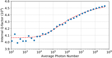
Figure 6. Internal Q-factor as a function of the average photon number occupation for the resonator with fundamental mode f = 6 GHz on sample vertical 1. The red dashed line shows a fit to a TLS power dependence. The weak change in Q indicates that the TLS have only a small contribution to the total loss rate even at the lowest powers.
Download figure:
Standard image High-resolution imageThe common TLS loss model [22] states that at high power (average number of photons much larger than the critical photon number,  ) the TLS loss rate becomes negligible compared to other losses. Moreover, a large temperature (T) compared with the resonator frequency can saturate the TLSs reducing their loss rate. The TLS loss as function of
  and T can be modelled as:

where  is the Q-factor due to the TLS at a very low temperature and photon number, and QA represents the Q due to all losses other than TLSs. The energy loss is due mainly to resonant TLSs, while non-resonant ones contribute to a frequency shift of the resonator frequency with respect to the temperature [30]).
From the fit shown in figure 6, we obtain  , close to the literature value for CPW resonators on low loss non-piezoelectric substrates such as silicon or sapphire. However, the value extracted for the high photon number is QA = 4.6 ± 0.5 × 10⁴, very far from the common values (≈106). This value is instead very close to our simulation of internal Qi from acoustic losses. The value β = 0.2 ± 0.02 is similar to those found in literature for non-piezoelectric substrates [31, 32]. A summary of these values for the different samples is reported in table 2.
Table 2. Average values and maximum dispersion errors resulting from the best fit function with equation (4).  is the internal quality factor due to the TLSs loss, nc is the average critical photon number and β is the exponent as shown in equation (4).
| Sample |  | β | nc (103) |
|---|---|---|---|
| Vertical 1 | 3.0 ± 1.4 | 0.19 ± 0.03 | 6 ± 6 |
| Vertical 2 | 3.3 ± 1.6 | 0.19 ± 0.06 | 10 ± 8 |
| Horizontal 1 | 1.2 ± 0.5 | 0.21 ± 0.02 | 4 ± 2 |
| Horizontal 2 | 1.2 ± 0.4 | 0.20 ± 0.04 | 6 ± 5 |
| Harmonics | 1.4 ± 0.03 | 0.16 ± 0.03 | 8 ± 9 |
Given these values, we can assume that the nature of resonant TLSs is the same as found on other substrates; and since the residual losses are larger than the TLS ones, we can conclude that the resonant TLSs are not the main loss mechanism for the resonators.
4.3. Temperature dependence of Qi and f
Finally, we study the temperature dependence of the internal quality factor and the resonator frequency. Here, the former provides information on the quasiparticle density, nqp, the latter has two contribution, non-resonant TLSs and quasiparticles.
Qi should decrease with an increase of temperature because nqp increases, leading to a larger resistive loss. Using the loss model from [11], Qi depends linearly on the density nqp:

where α is the ratio between the kinetic and total inductance of the resonator for kBT ≪ hfr, Δ is the aluminium superconducting gap, D(EF) is the density of states at the Fermi level, and QB is the quality factor due to all other losses than quasi particles.
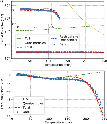
Figure 7(a) shows the fit of the measured Qi for a resonator of sample vertical 1 to equation (5) where also the TLS temperature dependence loss has been taken into account. We can extract the kinetic inductance ratio α = 1.35 × 10⁻³. Moreover the residual and mechanical losses dominate the dissipation with QB = 3.06 × 10⁴. Since this value is very close to the numerical evaluation of the mechanical Q factor, we can assume that the quasi particles are not the main loss factor for the resonators at low temperature.
Figure 7. Temperature dependence of Qi and resonance frequency of the resonator with fr = 4.356 GHz on sample vertical 1 measured at 107 photons: the increase in equilibrium quasiparticles produces a larger resistive loss rate (lower the internal Q) and an additional contribution to the total inductance (lowering the frequency). (a) The measured Qi values are fitted to an equilibrium quasiparticles distribution (orange dashed line). The green dashed line is the temperature depends TLS loss (equation (4)) with the parameters extracted from figure 6. The residual and mechanical contributions are shown in the blue dashed line. (b) Frequency shift of fr as a function of temperature; for T < 100 mK the main contribution to the frequency shift is due to non resonant TLS. The calculation of the TLS frequency shift (equation (6)) is shown in the plot (green dashed lines). For T > 100 mK the quasiparticles increase the kinetic inductance and become the main contributor to the frequency shift.
Download figure:
Standard image High-resolution image
The frequency fr of the resonators shifts because of two contributions: the first is due to the asymmetrically saturated spectral density that the TLSs give rise to. This effect is described by the TLS loss model [30]:

where Ψ is the digamma function. We can plot this function using the  extracted from the previous fit; the results are shown in figure 7(b). The second contribution is due to the equilibrium quasiparticle density that increases the kinetic inductance becoming the main factor for the frequency shift:

where  . An increase in temperature corresponds to an increase in quasiparticles density, causing a red shift in frequency.
In figure 7(b), we plot equation (7) using the kinetic inductance ratio obtained from the fit of equation (5). The result agrees well with the data for temperature above 100 mK. The sum of the two contributions is plotted with a red dashed line.
5. Discussion and conclusion
According to our results, the internal quality factor of CPW resonators on GaAs is mainly limited by the conversion of the photons stored in the resonator to mechanical waves (acoustic phonons) that dissipate energy into the substrate. We find that Qi increases as a function of frequency, as we numerically predicted. Although a direct measurement of the SAW and BAW generation was not performed, the match between the simulations and the measurements confirms our conclusion. In addition, we exclude the other most common loss sources by measuring the loss as a function of temperature and photon number in the resonator.
Future refinement of our simulation could include phonons scattering by the back surface of the chip. In our geometry, the very small difference between simulated and measured Qi suggests that this effect does not have a large contribution. Although, in general, this may not be the case for different geometries or devices.
We believe that this work can help improving designs and performance of superconducting devices built on piezoelectric substrates. We want to stress that, in the case of superconducting electronics, also in the single photon regime, an oscillating electric field generates mechanical waves due to the electromechanical coupling. Therefore, the lifetime of the excitations in these circuits will be limited by this conversion. According to our simulation, the magnitude of the photon to phonon conversion depends linearly on the electromechanical coupling and a geometry related factor. For example, similar simulations for resonators fabricated lithium niobate, have a much smaller internal quality factor than those we measured on GaAs.
One possible solution to limit this conversion is to design and fabricate phononic mode structures on the substrate to engineer phononic bandgaps. Alternatively, one can minimize the microwave circuitry fabricated on piezoelectric substrates to what is strictly needed in the experiment, either by using two chips in a flip chip geometry [16, 18] or by using piezoelectric thin films which can be selectively etched in designed regions [33].
Our model can simulate the generation of mechanical waves in all these configurations. Moreover, following the same procedure, we can calculate the reduction of the effective electromechanical coupling and consequently optimize the geometry that minimize the mechanical losses.
Acknowledgments
We wish to express our gratitude to Lars Jönsson for making the sample holder and to Avgust Yurgens for fruitful discussions regarding the manuscript. We gratefully acknowledge the financial support from the Swedish Research council and the Knut and Alice Wallenberg Foundation. This work was performed in part at Myfab Chalmers.