
Abstract
Adiabatic superconductor logic (ASL) families are energy-efficient because they can operate with a switching energy much less than the IcΦ0 product, where Ic is the critical current for Josephson junctions, Φ0 is the flux quantum, and IcΦ0 is generally on the order of 10–19 J. A switching energy of 0.03IcΦ0 has been demonstrated by adiabatic quantum-flux-parametron (AQFP) logic, which indicates the possibility of extremely energy-efficient digital circuits using ASL. ASL uses signal transformers to propagate and invert the signal current; otherwise, it is difficult to design inverters. However, signal transformers are generally difficult to miniaturize. Therefore, to realize high-density and energy-efficient superconductor circuits, ASL that does not use signal transformers is required. In this paper, we propose ASL without signal transformers, which we call directly coupled quantum-flux-parametron (DQFP). DQFP logic is based on AQFP, but it can invert signal current without using signal transformers. We conducted numerical simulation of a DQFP inverter chain to show that DQFP logic can invert signal current without signal transformers, and that DQFP logic can operate adiabatically. Then, we designed and fabricated basic DQFP circuits, such as an inverter chain and a full adder. All the circuits were found to have wide operating margins. Our results indicate that DQFP logic is suitable for high-density and energy-efficient superconductor circuits.
Export citation and abstract BibTeX RIS

Original content from this work may be used under the terms of the Creative Commons Attribution 4.0 license. Any further distribution of this work must maintain attribution to the author(s) and the title of the work, journal citation and DOI.
1. Introduction
Superconductor logic families [1–4] can operate with low power consumption at cryogenic temperatures, and thus are crucial in building cryogenic systems, such as single-photon image sensors [5–7] and quantum computers [8–10], in which superconductor digital circuits can be used as interface circuits for superconductor detectors or qubits. In general superconductor logic, the switching energy (energy dissipation per switching event) is approximately IcΦ0, where Ic is the critical current for Josephson junctions and Φ0 is the flux quantum; IcΦ0 is only 3.1 × 10⁻¹⁹ J for a typical Ic of 150 μA. To achieve even smaller switching energy, adiabatic superconductor logic (ASL) families, which adopt adiabatic switching [11, 12], have been proposed. ASL includes the parametric quantron [11, 13], quantum flux parametron (QFP) [14], negative-inductance superconducting quantum interference device (nSQUID) [15], and adiabatic QFP (AQFP) [16], which is a version of QFP that uses Josephson junctions with small characteristic times (on the order of sub-picoseconds) to reduce energy dissipation. In ASL, the potential energy of a logic gate changes gradually from a single well to a double well such that the logic state can change quasi-statically and adiabatically, which results in a switching energy much less than IcΦ0. A switching energy of 0.03IcΦ0 has been demonstrated with AQFP logic [17], indicating the possibility of extremely energy-efficient digital circuits using ASL.
ASL generally uses transformers (which we call signal transformers) to propagate and invert the signal current because magnetically coupled rf superconducting quantum interference devices (SQUIDs) are used as building blocks; otherwise, it is difficult to design inverters, as will be shown later. However, the signal transformers in ASL have the following problems. It is difficult to miniaturize transformers while maintaining coupling coefficients [18]. Also, in some logic such as AQFP, a signal transformer occupies a large part of the gate area [19]. Therefore, to realize high-density and energy-efficient superconductor circuits, ASL that does not use signal transformers is required. Rylov et al proposed DC powered parametric quantron [20] as ASL without signal transformers, which, however, was not practical due to narrow parameter margins. We showed that AQFP with π Josephson junctions can operate without using signal transformers [21], where rf-SQUIDs with π Josephson junctions are used to invert signal current. However, this approach is not possible using conventional fabrication processes for superconductor/insulator/superconductor Josephson junctions.
In this paper, we propose ASL without signal transformers, which we call directly coupled QFP (DQFP). DQFP logic is based on QFP/AQFP but can invert the signal current without using signal transformers. First, we show a typical schematic of an AQFP gate and explain why signal transformers are required in AQFP logic. Then, following an explanation of the operating principle of DQFP logic, we conduct numerical simulations of a DQFP inverter chain to show that the DQFP inverter can operate without signal transformers. We also show how other DQFP logic gates are designed. Finally, we demonstrate basic DQFP circuits, including an inverter chain, a buffer chain, a NOR gate, and a full adder.
2. Operating principle
Figure 1 schematically illustrates an AQFP gate. This gate is powered and clocked by an ac excitation current Ix, which produces an ac magnetic flux with an amplitude of 0.5Φ0. The combination of Ix and a dc offset current Id, which produces a dc magnetic flux of 0.5Φ0, allows AQFP circuits to be operated using only two ac current sources. The details of the excitation methods in AQFP logic can be found in the literature [19]. When Ix increases and a total magnetic flux of 0.5Φ0 is applied to the gate, either of the Josephson junctions J1 and J2 switches, depending on the polarity of the input current Iin. As a result, a state current Ist, the polarity of which represents the logic state, is generated through Lq; a positive Ist represents a logical 1, and a negative Ist represents a logical 0. Finally, the output current Iout is generated via a signal transformer composed of Lq, Lout, and kout. The logic function of this gate is determined by the polarity of kout. This gate operates as a buffer for a positive kout because the polarity of Iout is the same as that of Iin. Conversely, this gate operates as an inverter for a negative kout because the polarity of Iout is opposite to that of Iin. Without signal transformers, it is difficult to design inverters because the polarity of Ist is the same as that of Iin. This is why signal transformers are needed in AQFP logic gates.

Figure 1. AQFP gate. When Ix increases, either J1 or J2 switches depending on the polarity of Iin. For a positive (negative) kout, the direction of Iout is the same as (opposite to) that of Iin: this gate works as a buffer (inverter).
Download figure:
Standard image High-resolution imageFigure 2(a) illustrates a DQFP inverter, which does not include signal transformers. The operating principle of this gate is the same as that of AQFP gates. When an ac excitation current Ix increases, either of the Josephson junctions J1 and J2 switches depending on of the polarity of the input current Iin. The logic state for this gate is represented by the polarity of the state current Ist, as with AQFP logic. A marked difference from the AQFP gate shown in figure 1 is that a dc-SQUID composed of J1, J2, L1, and L2 is inserted between the input and output ports in figure 2(a), whereas a dc-SQUID is inserted between the input port and ground in figure 1. Therefore, Ist is output from the opposite side of the dc-SQUID to which the input current Iin is applied, whereas Ist and Iin share the same side of the dc-SQUID in the AQFP gate. As a result, the polarity of Ist is opposite to that of Iin after J1 or J2 switches: the DQFP gate shown in figure 2(a) operates as an inverter, even without signal transformers. It is noteworthy that Lq1 and Lq2 are added to make a closed loop composed of Lq1, Lq2, and the dc-SQUID; otherwise, the LIC product, or the potential energy shape, for the DQFP inverter changes significantly depending on the circuits connected to the DQFP inverter. Figure 2(b) illustrates a buffer used in DQFP logic, which is an AQFP gate with the signal transformer removed. The circuit parameters for the DQFP inverter and buffer are given in the caption of figure 2. The device parameters, such as sub-gap resistance, are based on the National Institute of Advanced Industrial Science and Technology (AIST) 10-kA cm−2 Nb high-speed standard process (HSTP) [19].

Figure 2. DQFP gates. (a) Inverter. L1 = L2 = 1.48 pH, Lq1 = Lq2 = 3.27 pH, Lin = 0.361 pH, and Lout = 0.806 pH. (b) Buffer, which is an AQFP gate without signal transformers. L1 = L2 = 1.44 pH, Lq = 5.40 pH, Lin = 11.9 pH, and Lout = 2.50 pH. The critical currents of J1 and J2 are 50 μA. J1 and J2 are not damped by resistors.
Download figure:
Standard image High-resolution image3. Numerical simulation
We conducted numerical simulations using the Josephson circuit simulator JSIM [22] to show that the DQFP inverter can invert a signal current without signal transformers. Figure 3(a) schematically illustrates the DQFP inverter chain used in the numerical simulations. This inverter chain is powered and clocked by a pair of ac excitation currents (Ix1 and Ix2) with a phase difference of 90° [19]. Ix1 and Ix2 cause an ac magnetic flux with an amplitude of 0.5Φ0 to be applied to each gate, and Id causes a dc magnetic flux of 0.5Φ0 to be applied to each gate. The frequency f of Ix1 and Ix2 corresponds to the given operating frequency. φ1 through φ4 represent excitation phases, by which logic operations are performed with a phase separation of 90°. Figure 3(b) shows the simulated waveforms of the DQFP inverter chain for f = 5 GHz, where Iin represents the input current to the first inverter and Ist1 through Ist4 represent the state currents [Ist in figure 2(a)] of the first through the fourth inverters, respectively. This figure shows correct operation because the logic state Ist is inverted by each DQFP inverter.

Figure 3. Transient analysis results for a DQFP inverter chain. (a) Schematic. The inverter chain is powered and clocked by Ix1 and Ix2. (b) Waveforms at 5 GHz. The logic signals are inverted by each DQFP inverter.
Download figure:
Standard image High-resolution imageWe also analyzed the switching energy for a DQFP inverter by integrating the product of the excitation currents and voltages over time [23]. Figure 4 shows the simulation results for the switching energy Esw as a function of f. The symbols are the simulation results, and the curve is a linear regression given by Esw = af, where f is in gigahertz and a = 1.14 × 10⁻²². This figure shows that Esw approaches zero as f decreases, that is, ΔF = W in the quasi-static limit, where ΔF is the free energy change of the DQFP inverter, and W is the work performed on the inverter by a power supply. Since the DQFP inverter does not conduct stochastic processes (i.e. entropy does not change), ΔF = ΔE, where ΔE is the energy change of the inverter. Thus, ΔE = W in the quasi-static limit, which indicates that the DQFP inverter can operate via quasi-static adiabatic processes.

Figure 4. Simulation results for the switching energy of a DQFP inverter. The switching energy approaches zero as the frequency decreases, which indicates that the DQFP inverter can operate adiabatically in the quasi-static limit.
Download figure:
Standard image High-resolution image4. Logic gate design
Since DQFP logic includes both inverters and buffers, DQFP logic gates can be designed in the minimalist way [24], where logic gates are designed using four types of building block cells: buffer, inverter, constant (which generates logical 0 s or 1 s), and branch (which is an inductor branch to merge or split the signal current). The constant cell can be designed by making the circuit parameters in the DQFP inverter (or buffer) asymmetrical [25]. Here we show an example of a minimalist design of DQFP logic gates. Figure 5(a) shows the layout of the DQFP inverter cell for the HSTP. The circuit parameters of the inverter were extracted using the 3D inductance extractor InductEx [26] and correspond to those shown in the caption of figure 2. This inverter adopts symmetrical layout to avoid unwanted parasitic magnetic coupling [24]. The area of this inverter is 20 μm (width) by 25 μm (height), which is only 62.5% of that of the AQFP inverter cell for the HSTP (width of 20 μm, height of 40 μm). This verifies that the gate area in ASL can be reduced by removing signal transformers. We also designed a DQFP buffer cell and a constant cell, the areas of which are the same as that of the DQFP inverter. Figure 5(b) shows how a three-input minority (MINO) gate cell, the output of which is determined by the minority vote of the inputs, is designed, where three DQFP inverter cells and a branch cell are put together. The output currents from the three inverter cells are merged by the branch cell, so that the output signal x is determined by x = (¬a ∧ ¬b) ∨ (¬b ∧ ¬c) ∨ (¬c ∧ ¬a), where a, b, and c are the input signals. Various logic gates can be designed on the basis of this MINO gate cell; for instance, a NOR gate can be designed by replacing one of the three inverter cells in the MINO gate with a constant-0 cell (which generates logical 0 s).

Figure 5. Layout of DQFP cells. (a) Inverter cell. The area is 20 μm (width) by 25 μm (height), which is 62.5% of that of an AQFP inverter. (b) MINO gate cell, which is composed of three inverter cells and a branch cell. The area is 60 μm (width) by 50 μm (height).
Download figure:
Standard image High-resolution image5. Experiment
We built a DQFP cell library that included various DQFP logic cells using minimalist design. Then, we designed basic DQFP circuits using the cell library, such as an inverter chain, a buffer chain, a NOR gate, and a full adder. This full adder was designed using three MINO gates in a way similar to previous studies [27, 28], which designed a full adder using three majority (MAJ) gates (which are complementary to MINO gates). Figure 6 shows a micrograph of these DQFP circuits fabricated using the HSTP, which includes Nb/AlOx/Nb Josephson junctions and four Nb layers on a Si substrate (more details can be found in the literature [19]). We have not designed readout circuits for DQFP logic, so we used AQFP circuits to read out the output signals of the DQFP circuits. The AQFP circuits receive the signal currents from the DQFP circuits, and the dc-SQUIDs coupled to the AQFP circuits generate voltage signals [16]. Ix1 and Ix2 are a pair of ac excitation currents to power and clock the DQFP circuits. Iina, Iinb, and Iinc are the input currents. The inverter and the buffer chains receive Iinc; the NOR gate receives Iinb and Iinc; and the full adder receives Iina, Iinb, and Iinc. Vinv, Vbuf, and Vnor are the output voltages of the inverter chain, buffer chain, and NOR gate, respectively; and Vcout and Vs are the carry-out and sum signals of the full adder, respectively. We operated the DQFP circuits at 4.2 K in liquid He. Figure 7 shows the waveforms measured at 100 kHz. All the circuits operated correctly with wide operating margins with regard to Ix1 and Ix2: ± 69% and ± 66% for the inverter chain, ± 41% and ± 39% for the buffer chain, ± 68% and ± 66% for the NOR gate, and ± 34% and ± 44% for the full adder. This experiment indicates that DQFP logic can operate robustly in actual circuits. Note that circuit performance is the same between AQFP and DQFP circuits because in both circuits the energy efficiency and operating frequencies are determined by junction parameters [29].
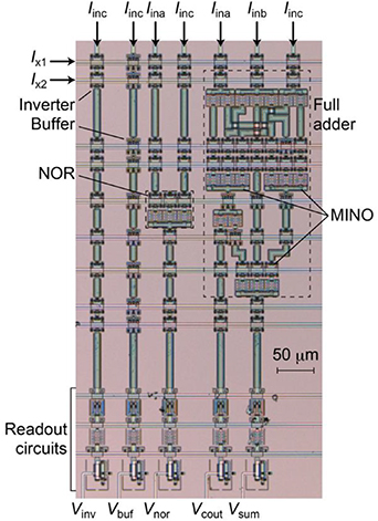
Figure 6. Micrograph of basic DQFP circuits, including an inverter chain, a buffer chain, a NOR gate, and a full adder. The circuits were fabricated using the HSTP.
Download figure:
Standard image High-resolution image
Figure 7. Measured waveforms at 100 kHz. All the circuits operated correctly with wide operating margins with regard to Ix1 and Ix2.
Download figure:
Standard image High-resolution image
6. Conclusion
We proposed ASL called DQFP, which does not have signal transformers. DQFP logic can achieve signal inversion without using signal transformers, which generally occupy a large area in conventional ASL gates and are difficult to miniaturize. The area of a DQFP inverter cell was only 62.5% of that of an AQFP inverter cell. Importantly, DQFP logic gates can be further miniaturized by adopting high-kinetic-inductance layers [30] in future fabrication processes, whereas the signal transforms in conventional ASL cannot use this approach because kinetic inductances do not couple to each other. Ultimately, the area of a DQFP inverter cell will be dominated by that of the dc-SQUID including J1 and J2 (approximately 15 μm by 10 μm) because the dc-SQUID requires a transformer to apply excitation flux; thus, it is estimated that the gate area will be reduced to only 19% of that of the current AQFP design (20 μm by 40 μm). We conducted numerical simulations to show that the DQFP inverter can operate without using signal transformers. We designed various DQFP logic gates using minimalist design to establish a cell library. We then designed and fabricated basic DQFP circuits, including an inverter chain, a buffer chain, a NOR gate, and a full adder. All the circuits were found to have wide operating margins with regard to excitation current. Our results indicate the possibility of creating high-density and energy-efficient superconductor circuits using DQFP logic.
Acknowledgments
The present study was supported by PRESTO (No. JPMJPR1528) from the Japan Science and Technology Agency (JST) and KAKENHI (No. 18H01493 and No. 19H05614) from the Japan Society for the Promotion of Science (JSPS). The circuits were fabricated in the Clean Room for Analog-digital superconductiVITY (CRAVITY) of the National Institute of Advanced Industrial Science and Technology (AIST). We would like to thank C J Fourie for providing the 3D inductance extractor InductEx.