

Abstract
This paper reports pulsed DC and RF characteristics of GaN high-electron-mobility transistors (HEMTs) on a silicon substrate under external mechanical tensile strain. Tensile strain enhanced two-dimensional electron gas (2DEG) density resulted in increasing ID, fT and fmax at CW measurement. Eliminating self-heating by pulse measurement, DC and RF characteristics between flat and bend devices were slightly increased for small-width devices, and decreased for wide-width devices. This was because maximum electron drift velocity was reduced by a hot phonon effect while 2DEG density increased by tensile strain for wide-width devices. Results indicated that the tensile strain on thinner substrates decreased the DC and RF performances of wide-width GaN-based RF power devices. This phenomenon should be considered while using GaN-based RF power devices for compact packages, especially in high-power applications.
Export citation and abstract BibTeX RIS
In recent years, GaN power transistors and integrated circuit technologies have been widely used in high-power and high-frequency communication systems. GaN devices can be grown on various substrates such as silicon carbide (SiC), sapphire, and silicon, which affect epilayer crystal quality of GaN and heat dissipation of transistor performance. Semi-insulating SiC has a very high thermal conductivity (4.9 W cm·K−1) and its lattice closely matches that of GaN, although it is costlier.1,2 A poor lattice match and lower thermal conductivity precludes the development of GaN on sapphire substrates.3,4 In recent years, the application of GaN to silicon substrate has become increasingly widespread due to its low cost, larger size, acceptable thermal conductivity, and ease of integration with complementary-metal-oxide semiconductor circuits.5,6 The challenges of GaN-on-silicon high-electron-mobility transistors (HEMTs) include lossy substrates and large thermal expansion coefficient mismatches between GaN and Si substrates.7 Several studies have reported the backgrind and backside metallization of HEMT on silicon substrate for compact packages and efficient heat dissipation.8–10 However, thin-down substrate results in wafer bowing and residual stress, affecting the piezoelectric polarization between GaN and AlGaN. Some literature has reported on the DC characteristic of HEMTs under mechanical tensile strain.11–13 Transient characteristics of HEMTs are also affected by external mechanical tensile strain.14,15 Strain-induced polarization change can be studied through examination of external mechanical strain. In this work, the mechanical tensile strain was applied by bending fixture to a curvature radii (r) of 2.5 and 1.5 cm. Deformation from external mechanical tensile strain of HEMT on 100 μm silicon substrate was studied using pulsed measurements of IV-characteristics and S-parameters. Wider width GaN transistors are widely used to provide high-power application; therefore, width dependence of HEMTs under tensile strain, including DC and RF performance, was also studied. Results showed external mechanical strain on wider width devices decreased the DC and RF performances should receive careful consideration, particularly in pulse measurement for high-power and high-frequency applications.
Device Structure and Mechanism
Figure 1a shows structures of the proposed HEMT grown on silicon using metalorganic chemical vapor deposition. The standard epilayers contained a 1.8-μm, unintentionally doped GaN buffer, a 0.8-μm GaN layer, an 18-nm Al0.27Ga0.73N barrier, and a 1-nm unintentionally doped GaN cap layer. Hall measurement showed a sheet carrier density of 1.03 × 1013 cm−2 and electron mobility of 1,534 cm2 V·s−1 at 300 K. The device was isolated by the mesa, which was constructed through an reactive-ion etching system. Ti-Al-Ni-Au multilayer metals were evaporated, followed by annealing to form ohmic contacts. A mushroom-shaped 0.5 μm gate was defined by a tri-layer resist scheme using Ni–Au metallization. Finally, the devices were protected with SiNx. After device fabrication was completed, the substrate was thinned to 100 μm, and the backside was ground-shielded using Aurum. Via-hole technology was used to connect the circuit ground to the backside. Five width devices with multi-finger topology (finger number (nr) × width: 2 × 25, 2 × 50, 2 × 75, 4 × 50, 4 × 75 μm) were used for measurements. Device characteristics were measured using pulsed-IV and pulsed-S-parameter on a flat and two bending fixtures in Fig. 1b. Figure 1c shows the schematic of the mechanical strain for measuring and calculating the mechanical strain of ε = 3 aF/btsub2E,16 where a is the shortest distance between the bending distance and the test device, F is the applied force for the die, b is the chip width, tsub is the wafer thickness, and E is the Young's modulus of the silicon (115 × 109 Pa). The curvature results in an additive tensile strain for devices on the top of bending fixture. The chip width of 1 cm on 100 μm Si substrate and 140 μm plastic under an applied tensile strain by bending fixture was calculated using ANSYS simulation software. The 15 mm and 25 mm radii of curvature give tensile strains of 0.034% and 0.02%, respectively.

Figure 1. (a) Cross-section view of AlGaN/GaN HEMT on silicon substrate. (b) The flexibility of the 100 μm thick Si substrate on bending fixture with curvature radius of 1.5 cm. (c) Schematic of the mechanical strain and the polarization fields in AlGaN and GaN layers applied by bending fixture. (d) Raman measurements for a GaN layer on silicon on a flat, r = 1.5 cm bending fixture.
Download figure:
Standard image High-resolution imageExternal mechanical strain of flat and bending GaN on silicon were characterized with Micro-Raman spectroscopy. Micro-Raman spectroscopy was performed to examined the strain effect, as shown in Fig. 1d. The E2 peaks of the GaN on silicon substrate were 568.8 and 567.6 cm−1 for flat and bending radius of 1.5 cm, respectively. The lower E2 was observed on r = 1.5 cm, which demonstrated that the mechanical strain applied in the GaN/AlGaN heterojunction was tensile. The external mechanical tensile strain affected the two-dimensional electron gas (2DEG) density of the devices, resulting in changing DC and RF performance, which requires further study.
Results and Discussion
DC characteristics
The difference in spontaneous polarization (PSP) due to strain from both band-discontinuous and piezoelectric polarization (PPE) between AlGaN and GaN heterojunctions induced 2DEG at the interface. The 2DEG density can be given as17
where P is total polarization, ε is the dielectric constant of AlGaN, d is the thickness of the AlGaN layer, ϕb is the Schottky barrier, EF is the Fermi level with respect to GaN conduction band edge energy, and ΔEC is conduction band offset at the AlGaN/GaN interface. Piezoelectric polarization is strain-induced because of the lattice mismatch between GaN and AlGaN. The strain from mechanical stress changes the atom locations resulting additional piezoelectric polarization.17 An additional mechanical strain that is proportional to strain and piezoelectric coefficients also generates piezoelectric polarization (PPEmech = eijε). The polarization fields in AlGaN and GaN layers applied by bending fixture are also shown in Fig. 1c. We assume the GaN layer is under full strain relaxation because the thickness of GaN layer is thicker than AlGaN layer (PPE,GAN = 0). Therefore, total polarization can be calculated by;18
The important HEMT parameter is saturated drain current, which can be written as17
where W is the channel width and vmax is maximum electron drift velocity. Therefore, saturated drain current is changed by 2DEG density, which is dependent on mechanical strain.
Figure 2 shows the drain current (ID) as a function of drain voltage (VD) using continuous-wave (CW) measurement for 2 × 50 μm- and 4 × 50 μm-wide AlGaN/GaN HEMT on a flat and two bending fixtures with r = 2.5 and 1.5 cm. ID was observed to increase as the radius decreased (strain increased) because the larger strain induced a higher 2DEG density, which corresponds with (3). According to obvious increased ID was inspected in larger strain, Fig. 3 shows CW and pulsed ID-VD for 2 × 50 μm- and 4 × 50 μm-wide devices on a flat and r = 1.5 cm bending fixture. To examine self-heating, pulsed-bias with CW and pulsed signals with pulse widths of 500 ns and 10 μs (fixed duty cycle at 0.1%) were compared. ID increased with decreasing pulse width because of improvement of the self-heating effect. ID was saturated at a pulse width of 500 ns, indicating that self-heating was eliminated. Figure 4a shows ID and normalized ID (ID to the device gate width, ID/W) at VD = 10 V and VG = 0 V as a function of gate width on a flat, r = 1.5 cm bending fixture. ID increased with pulse as width decreased. However, normalized ID slightly decreased with gate width due to a current crowding effect. The current crowding effect was also slightly improved as pulse width decreased.
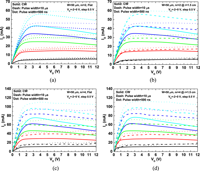
Figure 2. CW ID-VD of AlGaN/GaN HEMT on a flat and two bending fixtures with r = 2.5 and 1.5 cm for gate width of (a) 2 × 50 μm and (b) 4 × 50 μm.
Download figure:
Standard image High-resolution image
Figure 3. CW and pulsed ID-VD of AlGaN/GaN HEMT on silicon for 2 × 50 μm on a (a) flat, (b) r = 1.5 cm bending fixture and 4 × 50 μm on a (c) flat, (d) r = 1.5 cm bending fixture.
Download figure:
Standard image High-resolution image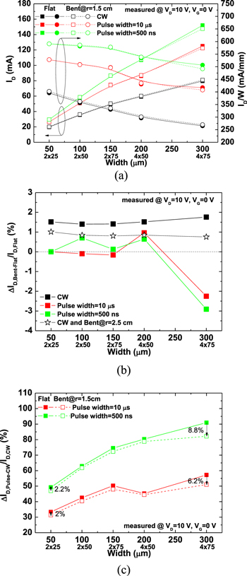
Figure 4. (a) ID and ID/W, (b) ΔID(Bent-Flat)/ID(Flat) (Stars stand for CW on r = 2.5 cm), (c) ΔID(pulse-CW)/ID(CW) as a function of gate width on a flat, r = 1.5 cm bending fixture for CW and pulse measurement.
Download figure:
Standard image High-resolution imageFigure 4b summarizes ΔID,Bent-Flat/ID,Flat vs gate width for strain analysis. ΔID,Bent-Flat/ID,Flat was calculated by subtracting ID measured by flat (ID,Flat) from ID measured by two bending fixtures (ID,Bent); ID,Flat was then normalized. For CW measurement, the average ΔID,Bent-Flat/ID,Flat for r = 2.5 and 1.5 cm were 0.85% and 1.52% and the standard deviations were 0.14% and 0.1% for all gate widths, respectively. ΔID,Bent-Flat/ID,Flat at CW increased with bending radius decreased, which demonstrates that 2DEG density increased with mechanical tensile strain increased. ΔID,Bent-Flat/ID,Flat at CW for all gate widths were close with small deviation, which indicates that the mechanical tensile strain dominates the increment rates of ID. For pulse measurements, ΔID,Bent-Flat/ID,Flat for r = 1.5 cm was nearly zero (even negative) at 10 μs pulse width for width = 50–150 μm (ID = 26–74 mA). A 0.96% ΔID,Bent-Flat/ID,Flat was obtained for 200 μm-wide device at 10 μs pulse width (ID = 87 mA). Even if self-heating was excluded (500 ns), ΔID,Bent-Flat/ID,Flat was still <1% for width = 50–200 μm (ID = 30–108 mA). ΔID,Bent-Flat/ID,Flat for pulse measurement was lower than that for CW measurement because trapping effect was observed.
However, ΔID,Bent-Flat/ID,Flat at 500 ns pulse was reduced to 0.65% for 200 μm-wide device, which is lower than that at 10 μs pulse width. ΔID,Bent-Flat/ID,Flat was also found to be lower at 500 ns (−2.9%) than that at 10 μs (−2.3%) for a 300 μm-width device. ΔID,Bent-Flat/ID,Flat was found to increase with pulse width decreasing for small-width devices (50–150 μm), whereas it was found to decrease with pulse width decreasing for wide-width devices (200 and 300 μm). These observations indicate that the hot phonon effect was occurred at high ID (≧108 mA) because the self-heating effect is significantly improved at shorter pulse width, resulting in lower ΔID,Bent-Flat/ID,Flat at 500 ns. Hot phonon caused stronger scattering effect and reduced drift velocity, thereby reducing ID.19,20 The stronger hot phonon effect for a 300 μm-width device (ID ≧ 125 mA) even resulted in the significant reduction in ID and a negative ΔID,Bent-Flat/ID,Flat. In addition, the hot phonon effect was not observed at low ID (<80 mA) for CW measurement, resulting in the increase in ID with tensile strain. The reduction in drain current via the hot phonon effect under larger tensile strain for wide-width devices cannot be neglected.
Figure 4c shows ΔID,pulse-CW/ID,CW as a function of gate width on a flat, r = 1.5 cm bending fixture. ΔID,pulse-CW/ID,CW was calculated by subtracting ID measured by CW (ID,CW) from ID measured by various pulse widths (ID,pulse), and then with a normalized ID,CW. Self-heating effect was significantly improved as device width increased and pulse width decreased. A 90.9% increment rate was even obtained on a flat device measured at a 500 ns pulse width. However, ΔID,pulse-CW/ID,CW was reduced by 1%–2% for devices with gate widths of 50–200 μm after bending. Significant degradation was also found with 300 μm-width devices. This observation indicates that trapping effect was occurred, resulting in lower ΔID,pulse-CW/ID,CW for bend devices. The difference of ΔID,pulse-CW/ID,CW between flat and bend devices were 6.2% and 8.8% at 10 μs and 500 ns pulse width, respectively. The larger degradation was found at shorter pulse width for wide-width devices. This, again, demonstrated that drift velocity was reduced at high 2DEG density by a hot phonon effect.19,20
RF characteristics
The unity gain cut-off frequency (fT) and maximum oscillation frequency (fmax) are two important parameters widely used to quantify transistor performance for RF applications. The following are well-known equations for fT and fmax21
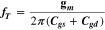
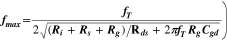
where gm is transconductance, Cgs and Cgd are the gate-to-source and gate-to-drain capacitances, and Ri, Rs, Rg, and Rds are channel, source, gate resistance, and output resistance, respectively. Figure 5 shows current gain and power gain as a function of frequency for AlGaN/GaN HEMT on silicon substrate, biased at maximum gm (gm,max) on a flat, r = 2.5 and 1.5 cm bending fixtures, measured by CW and a pulse width of 10 μs. We extracted fT and fmax at gm,max to ensure maximum value of fT and fmax for all gate width devices. The 500 ns cannot be shown due to instrument limitation for large-sized devices. Current gain followed the typical −20 dB sec−1 slope with increasing frequency, to extract fT at 0 dB, and power gain rolls to 1, to extract fmax. Figure 6 shows the fT and fmax as functions of gate width for comparison. At CW measurement, fT and fmax decreased with gate width, which was consistent with normalized ID. fT and fmax is slightly increased with tensile strain increasing at CW, which indicated that 2DEG density increased. The increment rates of fT between flat and bent at r = 1.5 cm devices (ΔfT,Bent-Flat/fT,Flat) at CW were very close (5.5 ± 1.7%) for gate widths from 50 μm–200 μm. Only a 1.2% increment rate of fT was found at CW for a 300 (4 × 75) μm-width device because of the significant self-heating effect. We do not discuss Δfmax here because fmax is estimated by the heterodyne method. For a 10 μs pulse width, fT and fmax for flat and bend devices were slightly increased with gate width increasing and was reduced for width ≧200 μm. This observation indicates that the self-heating effect is significantly improved, particularly for the gate width of 100–200 μm. Slightly higher fT and fmax were found after bending for small-width devices at 10 μs pulse width because the 2DEG density increased under tensile strain. Conversely, fT and fmax were slightly lower after bending for wide-width devices because hot phonon effect was observed, which was consistent with ID. fT can also be written as vmax/2πLg instead of gm to CgWvmax.22 Therefore, fT decreased with decreasing vmax because the larger tensile strain induced the hot phonon effect and reduce the drift velocity, as did fmax. Additionally, the rate of decrease of fmax as a function of gate width was larger than that of fT for CW and pulse measurement since ohmic losses related to resistive parasitic elements cannot be neglected,23 which corresponds with (5). Mechanical tensile strain increased 2DEG density as demonstrated by the increased DC and RF performances at CW measurement. However, DC and RF performances were degraded at pulse measurement because higher 2DEG density decreased maximum drift velocity through a hot phonon effect,20 this was significant for wider width devices. Tensile strain decreased the DC and RF performances of wide-width GaN-based RF power devices should be carefully controlled on thinner substrate for compact packages.
Figure 5. The frequency response of current gain and power gain for AlGaN/GaN HEMT with gate width of (a) 2 × 25 μm, (b) 2 × 75 μm, and (c) 4 × 75 μm for on a flat, r = 1.5 cm bending fixture for CW and pulse measurement. Symbols stand for CW on r = 2.5 cm.
Download figure:
Standard image High-resolution image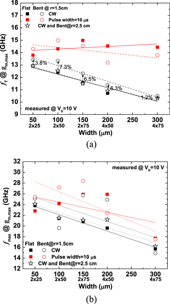
Figure 6. (a) ft and (b) fmax as a function of gate width on a flat, r = 1.5 cm bending fixture for CW and pulse measurement. Stars stand for CW on r = 2.5 cm.
Download figure:
Standard image High-resolution image
Conclusions
In this work, we analyzed tensile strain effect on GaN HEMT on silicon substrate using pulsed-IV and pulsed-S-parameter. These results demonstrated that 2DEG density increases with mechanical tensile strain at CW measurement. DC and RF performance improved via pulse measurement because of the improved self-heating effect. Lower increments, or even a degradation of DC and RF characteristics were found on tensile strain devices by a hot phonon effect while self-heating was excluded by pulse measurement. Hot phonon effect cannot be neglected for III-V compound semiconductors, especially for GaN-based RF power devices. This suggests that DC and RF characteristics should be monitored in GaN HEMTs for compact packages, especially in wide-width transistors for high-power applications.
Acknowledgments
The authors thank the Centre for Reliability Sciences and Technologies at Chang Gung University for their help. This work was partially supported by the Ministry of Science and Technology, Taiwan (no. 108-2221-E-182-024 & no. 108-2622-E-182-002-CC2) and the Chang Gung Memorial Hospital, Taiwan (BMRP957 & CMRPD2K0041).