
Abstract
We report on comparative studies of the optical vortex-induced structures of both Si(100) and Si(111) by irradiation with a single optical vortex picosecond pulse. Furthermore, we address the effects of the total angular momentum (TAM) on the optical vortex-induced microneedle. Si(111) allows for the faster growth of the microneedle, although this impacts the monocrystallization of the needle. The TAM then forces the melted silicon to spin axially, thereby yielding an efficient accumulation of melted silicon on the substrate for microneedle formation. These results provide new fundamental insights into the interactions between optical vortex fields and irradiated materials.
Export citation and abstract BibTeX RIS

Content from this work may be used under the terms of the Creative Commons Attribution 4.0 license. Any further distribution of this work must maintain attribution to the author(s) and the title of the work, journal citation and DOI.
Monocrystalline silicon (Si) is known as a standard material for general electronics and photonics, and it has been widely investigated. The formation of nano/microscale Si structures could potentially offer a novel degree of freedom for the development of various photonic devices, such as photonic crystals,1,2) photonic integrated circuits,3,4) and photovoltaic cells.5,6)
An optical vortex7–11) possesses various unique features, such as an orbital angular momentum (OAM) and an annular spatial form, due to its helical wavefront, which is characterized by a 2ℓπ azimuthal phase shift on-axis (ℓ is termed a topological charge). Optical vortices have thus been applied to various fields, not only in optical trapping and manipulation,12,13) quantum and optical communications,14,15) but also in materials sciences and related technologies.16–25)
The optical vortex enables radial inward mass transport of an irradiated material to be induced by vaporization-induced recoil pressure26) and thermal diffusion effects associated with its annular intensity profile, and the irradiated materials are collected within its dark vortex core to form nano/microscale structures, such as needles and helical structures. Several researchers have successfully demonstrated the formation of various Si structured materials by irradiation with optical vortices with pulse durations ranging from nanoseconds to femtoseconds.27–31) For instance, a single nanosecond to femtosecond optical vortex pulse with a low pulse energy (near ablation threshold) enables the formation of helical structures with the aid of spin angular momentum (SAM), characterized by s that originates from the circular polarization. A single picosecond optical vortex pulse with relatively high energy also allows for the fabrication of non-twisted nanoneedles.28)
Two types of Si substrates, oriented along (100) and (111), are employed as standard materials. The (100)-oriented Si substrate [Si(100)], mostly used in the previously cited studies, has a simple 2 × 1 reconstructed structure based on dimer structures. The resulting structured materials thus have rather high crystallinity, i.e. monocrystalline properties, as reported previously.27) The (111)-oriented Si substrate [Si(111)] has a rather complicated 7 × 7 constructed surface, the so-called dimer-adatom-stacking fault (DAS), with corner holes. Si(111) also allows for faster epitaxial growth than with Si(100), which is associated with its low surface free energy.
Here, we report comparative studies on the optical vortex-induced structures of both Si(100) and Si(111) by irradiation with a single optical vortex picosecond pulse. This research will provide fundamental insights in surface science and crystal engineering, and it may also offer entirely unique structured materials for industrial applications.
Figure 1 shows a schematic illustration of the experimental setup employed in this work. A monocrystalline Si(111) substrate (10 × 10 × 2 mm) was used as a target. A Q-switched, mode-locked Nd:YAG laser (B. M. Industries, Series 5000) was used with a wavelength of 1064 nm, a repetition frequency of 10 Hz, and a pulse width of 20 ps, and its output was converted to a right-handed (clockwise) circularly polarized optical vortex with ℓ = 1 and s = 1 [total angular momentum (TAM), assigned by J, is defined as the sum of OAM and SAM; J = ℓ + s = 2] using a spiral phase plate with a 2π azimuthal phase and a quarter wave plate (QWP). The circularly polarized optical vortex was loosely focused to be an annular spot with a diameter of approximately 70 μm by an objective lens (Mitutoyo M Plan Apo NIR 20×, NA = 0.2) onto the target at room temperature and atmospheric pressure. The effective NA of the focusing optics was thus estimated to be less than 0.1.

Fig. 1. (Color online) Schematic illustration of the setup for Si structure fabrication by irradiation with an optical vortex pulse.
Download figure:
Standard image High-resolution imageThe structured materials were then formed by irradiation with a single optical vortex pulse. All structures were observed by using a scanning electron microscope (SEM) with a spatial resolution of 8 nm.
Irradiation with the optical vortex pulse at an energy of >0.3 mJ enabled the fabrication of a Si(111) microneedle. It is worth noting that the polarization states of the irradiated optical vortex pulse did not contribute significantly to ablation performances, such as ablation threshold and melted volume of silicon,32) under this focusing condition. Irradiation of the circularly polarized optical vortex exhibited the ablation threshold (∼2.6 μJ) determined by employing the crater method.28) In fact, this value was almost the same as that (∼2.9 μJ) in irradiation of the linearly polarized optical vortex (Fig. 2).
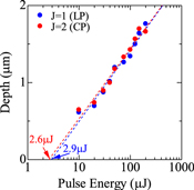
Fig. 2. (Color online) Measured depth of the fabricated crater versus the irradiated optical vortex pulse energy. Ablation threshold of the Si substrate was determined by employing the crater method.
Download figure:
Standard image High-resolution imageAs previously reported, Si(100) microneedles exhibit typically high crystallinity (monocrystalline properties); however, the Si(111) microneedle was formed of multiple domains, which were observed by employing X-ray diffraction (XRD) [Figs. 3(a) and 3(b)]. The optical vortex pulse energy was then measured to be 0.8 mJ.
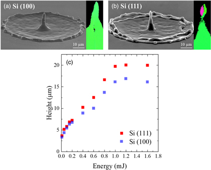
Fig. 3. (Color online) SEM and XRD images of fabricated Si needles. The colored region in XRD images indicates a crystal domain; therefore, the (a) Si(111) microneedle is polycrystalline, while the (b) Si(100) microneedle is monocrystalline. (c) Experimental height of the fabricated Si microneedles as a function of the irradiated vortex pulse energy. Figure (a) is reproduced with permission from28) © 2016, Springer Nature.
Download figure:
Standard image High-resolution imageThe increase of the irradiated pulse energy further caused an increase in the height of the fabricated microneedle. The microneedle had a height of 20 μm at a pulse energy of 1.6 mJ, which was approximately 1.25 times higher than that fabricated on Si(100) [Fig. 3(c)]. Further higher energy pulse deposition prevented the further growth of microneedle mainly owing to the vaporization of the silicon.
The free energy barrier generally required for nucleation under thermal equilibrium is proportional to the cube of the surface energy.33) Si(111) enables the fast growth of a defect-rich needle associated with its relatively low surface energy (1.24 J m−2, cf. 1.40 J m−2 on Si(100)34,35)). Si(111) with DAS will impact the monocrystallization of the microneedle. The resulting microneedle is thus polycrystalline with multiple domains. Helical cone-shaped structures with rich defects on the conical surface can also be fabricated by employing a relatively high energy pulse of 0.2–0.3 mJ. In comparison, only low pulse energy below 0.2 mJ permitted the formation of a helical Si(100) structure. Helical rate was defined as the number of fabricated helical structures divided by the number (30) of fabricated structures, and it represented the probability (%) of fabricating helical structures with respect to total number of fabricated structures. In fact, the helical rate was 1.1–3.1 times higher than that of Si(100) at pulse energies within the range of 0.01–0.2 mJ [Figs. 4(a)–4(c)].
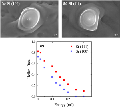
Fig. 4. (Color online) SEM images of helical structures of (a) Si(100) and (b) Si(111) fabricated by irradiation with a right-handed optical vortex pulse. (c) Measured helical rate of fabricated structures as a function of the irradiated optical vortex pulse energy.
Download figure:
Standard image High-resolution imageThe overlaid vortex pulses further accelerated the growth of the microneedle, as shown in Fig. 5. The pulse energy was then fixed to 0.8 mJ. The resultant microneedle had a height of approximately 47 μm, and its thickness, defined as the full-width at 50% height of the needle, was approximately 16 μm by irradiation with 24 overlaid pulses. The corresponding volume of the microneedle was estimated to be 2.7 times that of the Si(100) microneedle, which is also supported by the low surface energy of Si(111). The fabricated microneedle should be brittle after undergoing several melting and crystallization processes. Thus, the excessive overlaid pulses induced the breaking or ablation of microneedle owing to the local heating effects, thereby preventing the further growth of microneedle. The further growth of microneedle might be possible by optimizing the focusing optics, for instance, further loosely focusing with high energy pulse to avoid the excessive local heating, as a future work.

Fig. 5. (Color online) (a) Experimental height and (b) thickness of the needles versus a number of overlaid optical vortex pulses.
Download figure:
Standard image High-resolution imageWe previously reported36) that the TAM typically determines the shape of fabricated microneedles. Experiments were performed by utilizing the optical vortex pulses with J = 0. The QWP was then reversed so that OAM and SAM cancelled each other to give zero TAM. Further growth of the microneedle was suppressed, and the height of the microneedle was limited to be 13 μm, even with an increase of the pulse energy. The experimental results are summarized in Fig. 6. These results suggest that the TAM of the optical vortex pulses causes the melted silicon to spin axially, thereby yielding an efficient accumulation of melted silicon on the substrate for microneedle formation.

Fig. 6. (Color online) SEM images of Si(111) microneedles fabricated by irradiation with optical vortex pulses with TAM of (a) J = 2 and (b) J = 0. (c) Measured height of Si microneedles as a function of the irradiated optical vortex pulse energy.
Download figure:
Standard image High-resolution imageIt is worth mentioning that the irradiated optical vortex produced HAZ with a width of ∼10 μm outside the ablated zone [see Fig. 6(b)], thereby inhibiting the fabrication of microneedles with high density of >1/(10 × 10 μm2). The microneedles with low density (∼50 μm pitch) can be easily fabricated only by translating the silicon substrate as shown in Fig. 7. High repetition frequency picosecond laser with PRF > 100 kHz might allow the mass-production of microneedles. As mentioned in our previous publication,28) the microneedle formation requires typically a microsecond time scale. Thus, the undesired residual heat on the substrate by high repetitive pulse deposition might impact the efficient solidification (crystallization) of the microneedle. Further investigation of such residual heat effects should be studied as a future work, though it is beyond the scope of this letter.

Fig. 7. (a) Side and (b) top views of microneedle array fabricated by irradiation of twelve overlaid optical vortex pulses with TAM of J = 2 and a pulse energy of 0.8 mJ.
Download figure:
Standard image High-resolution image
We have investigated the microneedle structuring of Si(111) by irradiation with picosecond optical vortex pulses. The Si(111) microneedle consists of multiple crystal domains and exhibits significantly faster growth than the Si(100) microneedle due to its low surface energy and defect-rich surface. The overlaid vortex pulses further accelerate growth of the microneedle. It should be noted that the fabricated Si(111) microneedle was twisted by irradiation with an optical vortex pulse with a pulse energy less than 0.3 mJ. These results provide new fundamental and advanced insight into the interaction between light fields with OAM and materials in crystal engineering.
Acknowledgments
The authors acknowledge financial support in the form of KAKENHI Grants-in-Aid (Nos. JP16H06507, JP17K19070, and JP18H03884) from the Japan Society for the Promotion of Science (JSPS) and a CREST grant (No. JPMJCR1903) from the Japan Science and Technology Agency (JST).