Pulsed Laser Deposition of In0.1Ga0.9N Nanoshapes by Nd:YAG Technique

1
Electronic Materials Research Department, Advanced Technology and New Materials Research Institute, City of Scientific Research and Technological Applications (SRTA-City), Alexandria 21934, Egypt
2
National Institute of Laser Enhanced Science, Laser Interaction with Matter Department, Cairo University, Cairo 94142, Egypt
*
Author to whom correspondence should be addressed.
Coatings 2020, 10(5), 465; https://doi.org/10.3390/coatings10050465
Submission received: 8 March 2020
/
Revised: 25 April 2020
/
Accepted: 5 May 2020
/
Published: 10 May 2020
(This article belongs to the Special Issue Design, Fabrication, and Characterization of Thin Films for Photonic Applications)
Abstract
:In0.1Ga0.9N thin film was grown on a cheap glass substrate by the Nd:YAG pulsed laser deposition technique. The In0.1Ga0.9N thin films show the semi-crystalline structure as observed with X-ray diffraction (XRD). The surface morphology has a non-dense layer with both scattered nanospheres and agglomerated particles. These nanospheres tended to grow randomly on the glass substrate, as observed with field emission scanning electron microscopy (FESEM). The direct bandgap energy for In0.1Ga0.9N thin film was 2.08 eV, which is calculated using photoluminescence (PL) measurements. The Raman measurements illustrated two sets of phonon modes as A1(LO) and E2 high vibrational modes that are observed. The resonance behavior of the A1(LO) mode is experimentally verified and studied under laser light energy of 532 nm.
1. Introduction
The III-nitrides, such as InN, GaN and AlN, have recently received great attention because of their major contribution to various optoelectronic applications such as light-emitting and laser diode applications [1]. The structures of these materials depend on the stoichiometry of the elements and preparation conditions [2]. The InxGa1−xN was driven by tailoring their bandgap according to the composition x [3]. The binary nitrides crystallize in the wurtzite (wz) structure and show the lowest direct optical transition across their fundamental band gaps of 0.7 eV (InN), 3.5 eV (GaN) and 6 eV (AlN) [4]. Thus, these alloys cover the electromagnetic spectrum from the infrared to the ultraviolet [5]. The InxGa1−xN thin films have been prepared by several techniques such as molecular beam epitaxy (MBE), hybrid vapor phase epitaxy (HVPE), and pulsed laser deposition (PLD) [6]. PLD is a highly non-equilibrium evaporation process, which can be operated at low temperature to increase indium incorporation [7]. Most of the InxGa1−xN targets used in PLD are fabricated by pressing the alloy powders at high pressure, followed by sintering at high temperatures [8]. From our previous work [9], InxGa1−xN bulk alloys have been prepared as a target by a simple novel method. III-nitride group has been deposited on sapphire (Al2O3), silicon, Sic and GaN which play an important role in the stoichiometry of the thin film substrates [10]. In this work, InxGa1−xN will be deposited for the first time by an Nd:YAG laser technique on glass substrate, giving a yellow emission that could be used in LED applications.
2. Material and Method
In0.1Ga0.9N film is grown on a glass substrate under a heating temperature of 250 °C in nitrogen plasma by an Nd:YAG laser technique. The target consists of In0.1Ga0.9N alloy mounted on a holder and it is prepared as illustrated in our previous work [11]. An Nd:YAG laser (Nd:YAG, Continuum Company pl9000, Boston, MA, USA) at λ = 532 nm was employed as the ablation source, and operated with a repetition rate of 10 Hz and pulse energy of 60 mJ. The working pressure was 1.13 × 10⁻⁴ Torr with the injection of N2 plasma, and the deposition time was 10 min. During the deposition process, the target was rotated at 25 rpm. The ablation laser was directed onto the target to generate In0.1Ga0.9N vapor. The structure and morphology of the In0.1Ga0.9N thin film were systematically analyzed by X-ray diffraction (XRD-Shimadzu XRD 7000 maxima powder diffractometer, Kyoto, Japan), field emission scanning electron microscopy (FESEM-Quanta 250, Hillsboro, OR, USA), photoluminescence (PL-Perkin Elmer Luminescence Spectrometer Model LSS, Waltham, MA, USA) and Raman spectroscopy (Raman Senterra II, Karlsruhe, Germany).
3. Results and Discussion
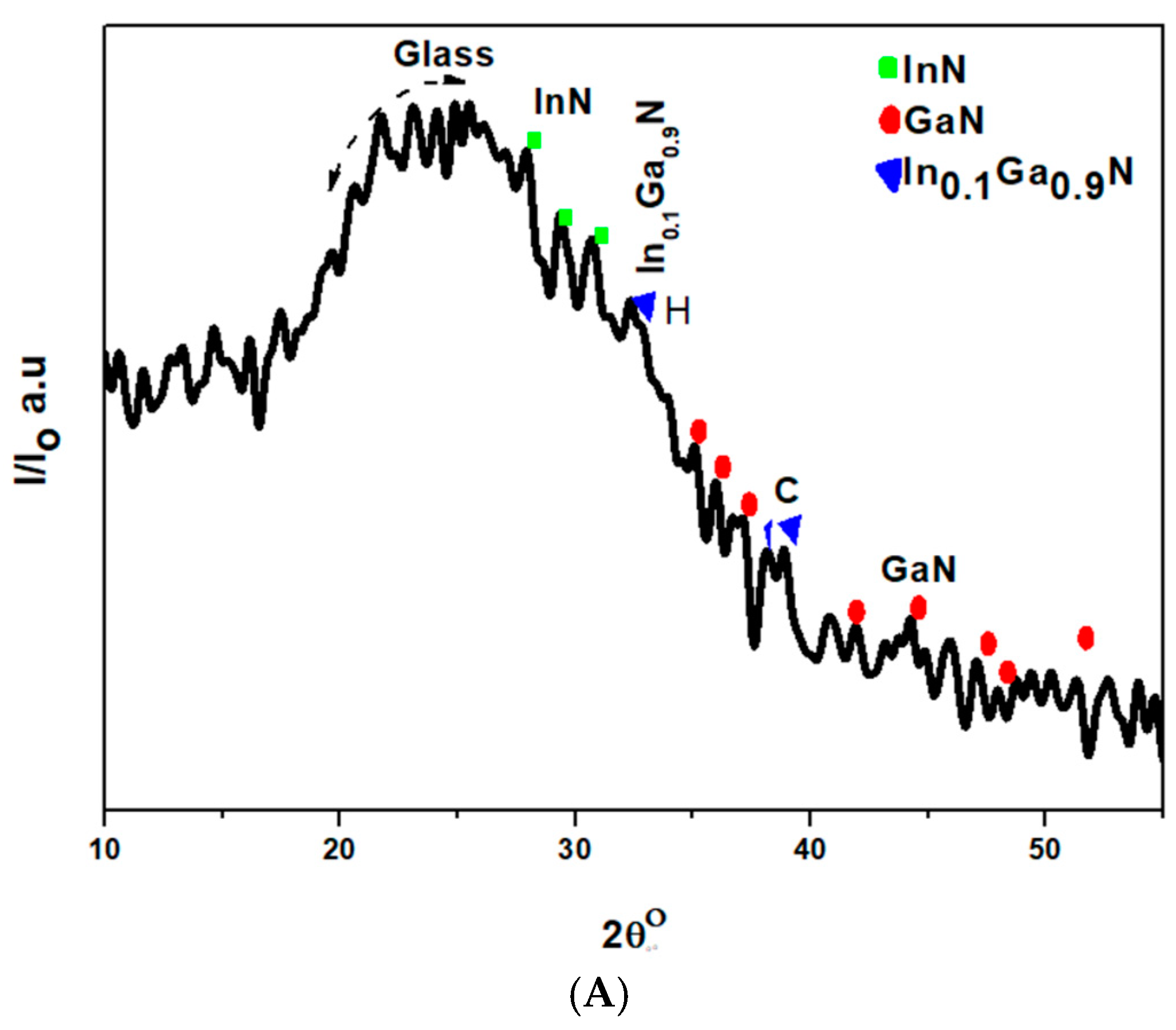
Semi-crystalline nature is observed for the studied material as shown in Figure 1A. The thin film exhibits diffraction peaks located at different angles for (GaN, InN, and In0.1Ga0.9N). GaN is located at 2Ɵ = 35.14°, 35.94°, 36.98°, 38.56° [PDF CARD 01-080-0011, Cubic]; [PDF CARD 01-079-2499, Hexagonal], [PDF CARD 01-076-0703,Hexagonal]; [01-079-2499, Hexagonal]. InN is located at 2Ɵ = 29.33° [PDF CARD 01-088-2362, Hexagonal] and In0.1Ga0.9N is located at 2Ɵ = 32.39° (Hexagonal), 38.18° (Cubic), 38.81° (Cubic), which is matched with the results of other works [12,13,14]. In PLD, a pulse from the ablation laser is impacted with the In0.1Ga0.9N target which is dissociated, so In and Ga vapors were reacted with the nitrogen plasma, resulting in the formation of InN, GaN and In0.1Ga0.9N as a result of the reaction between indium and Gallium vapors [15]. The average crystallite size of the particles is 1.17 nm, which is calculated for 2Ɵ = 32° by Scherer’s equation [16]:
D = 0.9 λ/β cosθ
Figure 1B shows the Raman spectra peak at 437.41 cm−1 for InN, which is slightly shifted from 431.41 to 437 cm−1 [17]. A broad peak at 538.9 cm−1 is observed, which is corresponding to GaN formation that is shifted from 533.9 cm−1.Two other peaks are observed; one peak at 621.98 cm−1 belongs to In0.1Ga0.9N (cubic), which is shifted from 617.98 cm−1 [18] and the second peak at 694.94 cm−1 belongs to In0.1Ga0.9N (cubic), which is shifted from 690.94 cm−1 [19]. The broad peak of 746.2 cm−1 belongs to In0.1Ga0.9N (hexagonal), which is shifted from 742.2 cm−1 [19]. The shifting process of Raman peaks may be referring to the strain in GaN, InN and In0.1Ga0.9N samples [20].
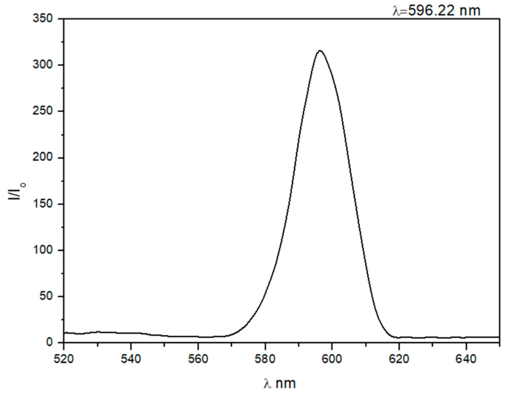
Figure 2 shows the PL spectra, which present one strong emission peak of In0.1Ga0.9N centered at 596.22 nm with a band gap of 2.08 eV. The PL peak is observed in the yellow region. The deposited In0.1Ga0.9N (with energy bandgap of 2.08 eV) shows a red shift of the visible PL form the bulk target alloy (Eg = 2.65 eV) [9]. This shift may be related to application of the Nd:YAG technique. Through the deposition process, the bulk material is heated and transferred into vapor phase with the same composition, and the nucleation process is started, and crystal growth [21] occurs on the glass substrate but with disordered distribution of elements on sites of the parent lattice. This disorder distribution has a deep effect on the band gap, which caused this reduction in the band gap value from its bulk state [22]. Thus, the conduction band edge is pushed down while the valence band edge is pushed upward, which causes a reduction of the band gap from 2.65 to 2.08 eV. Additionally, the strain and relaxation may cause a mismatch between the deposited layer and substrate and have an effect on the energy gap of the deposited thin film [22].
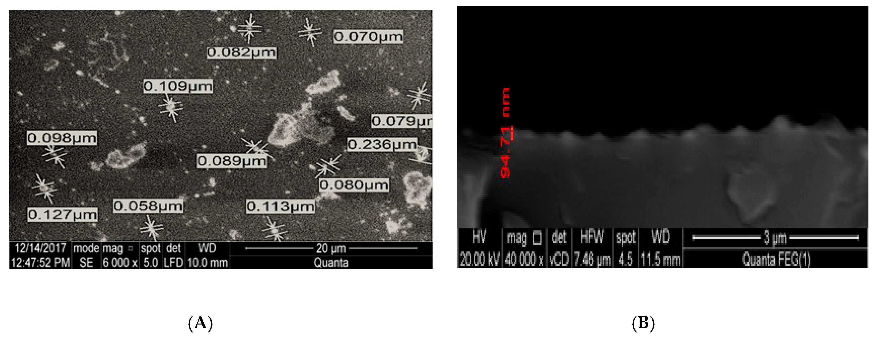
Figure 3A shows the surface morphology of the In0.1Ga0.9N Bulk alloy (order distribution) [9] and deposited layer on glass substrate, with bright spots standing out against a darker background (disorder distribution). From our previous work [9], the bulk material had a nanowire structure with diameter of 69 nm and length of 341 nm. Moreover, the morphology of the film is not very dense, is free of cracks and has a relatively inhomogeneous distribution. The average grain sizes are in the range of 79.43 nm, which is determined by using image analyzer software. The film thickness is 94.7 nm. The difference between the XRD crystallite size calculated and FESEM may be due to the nature of the particles themselves that are agglomerated, having dense particles in some areas of the thin film.
The chemical composition of the film is examined using EDX analysis as shown in Table 1. The weight percent of the composition of In0.1Ga0.9N is doubled to the calculated one. There is an excess of indium and a decrease of gallium, because the evaporation temperature of In is less than the evaporation temperature of gallium, which appears clearly in the difference between the large lattice mismatch between InN and GaN. This is confirmed by the XRD results according to the semi-crystalline nature of the thin film [23,24].
4. Conclusions
We reported the fabrication of In0.1Ga0.9N thin film using a Nd:YAG laser technique, which preserved a semi-crystalline structure with both hexagonal and cubic phases. FESEM images show agglomerated nanoparticles with an average grain size of 79.43 nm. PL concludes that there is a large emission peak with a distinctive yellow band. Raman spectra prove the strain of the In0.1Ga0.9N through the peak shift from 746.2 to 742.2 cm−1. Future work will involve the use indium composition (x ≥ 0.2) in order to tolerate the InxGa1−xN band gaps, which are of importance for optoelectronic, sensor and photovoltaic applications.
Author Contributions
A.E.-H.B.K. and M.F. proposed the research procedure and the characterization plan; S.G. conducted the experiments; A.E.-H.B.K., M.F., and S.G. designed and constructed figures and table; Y.B. supervised the Nd:YAG experiments; A.E.-H.B.K., M.F., Y.B., and S.G. analyzed and interpreted the data, and wrote the manuscript. All authors have read and agreed to the published version of the manuscript.
Funding
This research received no external funding.
Acknowledgments
This work was carried out at City for Scientific Research and Technological Applications (SRTA-City) and collaboration research with the National Institute of Laser Enhanced Science. The work of Nd:YAG laser supported by National Research Centre DrAymanDarwish.
Conflicts of Interest
The authors declare no conflict of interest.
References
- Xue, J.; Cai, Q.; Zhang, B.; Ge, M.; Chen, D.; Chen, J.; Zhib, T.; Wang, L.; Zhang, R.; Zheng, Y. Structural characterization of InGaN multi-quantum-wells grown on high indium content InGaN template with {1 0 1¯m} faceted surface. Mater. Lett. 2017, 208, 19–22. [Google Scholar] [CrossRef]
- Amano, H. Progress and prospect of the growth of wide bandgap group III nitrides: Development of the growth method for single-crystal bulk GaN. Jpn. J. Appl. Phys. 2013, 52, 050001. [Google Scholar] [CrossRef] [Green Version]
- Specht, P.; Kisielowski, C. On the chemical homogeneity of InxGa1−xN alloys—Electron microscopy at the edge of technical limits. Mater. Sci. Semicond. Process. 2017, 65, 24–34. [Google Scholar] [CrossRef]
- Li, J.; Nam, K.; Nakarmi, M.; Lin, J.; Jiang, H. Band structure and fundamental optical transitions in wurtzite AlN. Appl. Phys. Lett. 2003, 83, 5163–5165. [Google Scholar] [CrossRef] [Green Version]
- Zou, Y.; Zhang, Y.; Hu, Y.; Gu, H. Ultraviolet detectors based on wide bandgap semiconductor nanowire: A review. J. Sens. 2018, 18, 2072. [Google Scholar] [CrossRef] [PubMed] [Green Version]
- Rahman, M.; Hasan, M. Compound semiconductor epitaxial growth techniques. IJTFST 2016, 5, 45–49. [Google Scholar]
- Sanguino, P.; Niehus, M.; Melo, L.; Schwarz, R.; Koynov, S.; Monteiro, T.; Soares, J.; Alves, H.; Meyer, B.K. Characterisation of GaN films grown on sapphire by low-temperature cyclic pulsed laser deposition/nitrogen rf plasma. Solid-State Electron. 2003, 47, 559–563. [Google Scholar] [CrossRef]
- Shen, K.; Wang, T.; Wuu, D.; Horng, R. High indium content InGaN films grown by pulsed laser deposition using a dual-compositing target. Opt. Exp. 2012, 20, 15149–15156. [Google Scholar] [CrossRef] [PubMed]
- Kashyout, A.B.; Fathy, M.; Gad, S.; Badr, Y.; Bishara, A.A. Synthesis of nanostructure InxGa1−xN bulk alloys and thin films for LED devices. Photonics 2019, 6, 44. [Google Scholar] [CrossRef] [Green Version]
- Chen, C.C.; Yeh, C.C.; Chen, C.H.; Yu, M.Y.; Liu, H.L.; Wu, J.J.; Chen, K.H.; Chen, L.C.; Peng, J.Y.; Chen, Y.F. Catalytic growth and characterization of gallium nitride nanowires. J. Am. Chem. Soc. 2001, 123, 2791–2798. [Google Scholar] [CrossRef]
- Wang, X.; Yoshikaw, A. Molecular beam epitaxy growth of GaN, AlN and InN. Prog. Cryst. Growth Charact. Mater. 2004, 48, 42–103. [Google Scholar] [CrossRef]
- Itoh, T.; Hibino, S.; Sahas, T.; Kato, Y.; Koiso, S.; Ohashi, F.; Nonomura, S. InXGa1−XN films deposited by reactive RF-sputtering. J. Non-Cryst. Solids 2012, 358, 2362–2365. [Google Scholar] [CrossRef]
- Murthy, V.; Srivani, A.; Raghavaiah, G. Physical studies in III-nitride semiconductor alloys. Int. J. Thin Film. Sci. Technol. 2017, 6, 15–27. [Google Scholar] [CrossRef]
- Guarneros, C.; Espinosa, J.; Sánchez, V.; López, U. Study of InxGa1−xN layers growth on GaN/Al2O3 by MOCVD at different pressures. Superf. Y Vacío 2013, 26, 107–110. [Google Scholar]
- Ohta, J.; Fujioka, H.; Honke, T.; Oshima, M. Epitaxial growth of InN on c-plane sapphire by pulsed laser deposition with r.f. nitrogen radical source. Thin Solid Film 2004, 457, 109–113. [Google Scholar] [CrossRef]
- Uvarov, V.; Popov, I. Metrological characterization of X-ray diffraction methods for determination of crystallite size in nano-scale materials. Mater. Charact. 2007, 58, 883–891. [Google Scholar] [CrossRef]
- Hernández, S.; Cuscó, R.; Pastor, D.; Artús, L.; O’Donnell, K.; Martin, R.; Watson, I.; Nanishi, Y.; Calleja, E. Raman-scattering study of the InGaN alloy over the whole composition range. J. Appl. Phys. 2005, 98, 1–5. [Google Scholar] [CrossRef] [Green Version]
- Abata, A.; Leite, J.; Lima, A.; Silveira, E.; Lemos, V.; Frey, T.; As, D.; Schikora, D.; Lischk, K. Raman scattering study of zinc blende InxGa1−xN alloys. Phys. Status Solidi 1999, 216, 1095–1097. [Google Scholar]
- Talnishnikh, N.; Ivanov, A.; Smirnov, A.; Shmidt, E.S.N. The contribution of the in distribution in InGaN/GaN MQW to the “green gap” phenomenon. J. Phys. Conf. Ser. 2019, 1199, 012015. [Google Scholar] [CrossRef]
- Sun, W.; Tan, C.; Tansu, N. III-nitride digital alloy:electronics and optoelectronics properties of the InN/GaN ultra-short period. Sci. Rep. 2017, 7, 1–8. [Google Scholar]
- Li, J.; Zhu, H. Chapter 1— Advances in III-V semiconductor nanowires and nanodevices. In Advances in III-V Semiconductor Nanowires and Nanodevices; Li, J., Wang, D., LaPierre, R., Eds.; Bentham eBooks: Sharjah, United Arab Emirates, 2011; pp. 3–21. [Google Scholar]
- Zhao, C.; Yu, L.; Tang, C.; Li, M.; Zhang, J. The factors influencing the band gap bowing of III nitride alloys. Adv. Mater. Res. 2011, 298, 13–19. [Google Scholar] [CrossRef]
- Sklute, E.; Kashyap, S.; Dyar, M.; Holden, J.; Tague, T.; Wang, P.; Jaret, S. Spectral and morphological characteristics of synthetic nanophase iron (oxyhydr)oxides. Phys. Chem. Miner. 2018, 45, 1–26. [Google Scholar] [CrossRef] [PubMed]
- Wall, C.; Stampf, C.; Neugebauer, J. Theory of doping and defects in III-Vnitrides. J. Cryst. Grow. 1998, 189, 505–510. [Google Scholar] [CrossRef] [Green Version]
Figure 1.
(A) XRD pattern and (B) RAMAN spectra (excited at 514 nm) of In0.1Ga0.9N thin film.


Figure 2.
PL of In0.1Ga0.9N thin film.

Figure 3.
(A) FESEM of In0.1Ga0.9N thin film prepared by Nd:YAG laser and (B) the cross section of the deposited thin film.
Figure 3.
(A) FESEM of In0.1Ga0.9N thin film prepared by Nd:YAG laser and (B) the cross section of the deposited thin film.


Table 1.
EDX results of In0.1Ga0.9N film.
| EDX | In% | Ga% | N% |
| 20.34 | 70.85 | 8.80 |
© 2020 by the authors. Licensee MDPI, Basel, Switzerland. This article is an open access article distributed under the terms and conditions of the Creative Commons Attribution (CC BY) license (http://creativecommons.org/licenses/by/4.0/).
Share and Cite
MDPI and ACS Style
Gad, S.; Fathy, M.; Badr, Y.; Kashyout, A.E.-H.B. Pulsed Laser Deposition of In0.1Ga0.9N Nanoshapes by Nd:YAG Technique. Coatings 2020, 10, 465. https://doi.org/10.3390/coatings10050465
AMA Style
Gad S, Fathy M, Badr Y, Kashyout AE-HB. Pulsed Laser Deposition of In0.1Ga0.9N Nanoshapes by Nd:YAG Technique. Coatings. 2020; 10(5):465. https://doi.org/10.3390/coatings10050465
Chicago/Turabian StyleGad, Sara, Marwa Fathy, Yehia Badr, and Abd El-Hady B. Kashyout. 2020. "Pulsed Laser Deposition of In0.1Ga0.9N Nanoshapes by Nd:YAG Technique" Coatings 10, no. 5: 465. https://doi.org/10.3390/coatings10050465
Note that from the first issue of 2016, this journal uses article numbers instead of page numbers. See further details here.