Infrared Absorption Study of Zn–S Hybrid and ZnS Ultrathin Films Deposited on Porous AAO Ceramic Support


1
Institute of Optoelectronics, Military University of Technology, Str. gen. Sylwestra Kaliskiego 2, 00-908 Warsaw, Poland
2
Department of Chemistry, University of Helsinki, P.O. Box 55, FI-00014 Helsinki, Finland
3
Institute of Materials Science and Engineering, Military University of Technology, Str. gen. Sylwestra Kaliskiego 2, 00-908 Warsaw, Poland
*
Author to whom correspondence should be addressed.
Coatings 2020, 10(5), 459; https://doi.org/10.3390/coatings10050459
Submission received: 21 April 2020
/
Revised: 5 May 2020
/
Accepted: 6 May 2020
/
Published: 9 May 2020
(This article belongs to the Special Issue Recent Advances in Metal, Ceramic, and Metal-Ceramic Composite Films/Coatings)
Abstract
:Infrared (IR) spectroscopy is a powerful technique to characterize the chemical structure and dynamics of various types of samples. However, the signal-to-noise-ratio drops rapidly when the sample thickness gets much smaller than penetration depth, which is proportional to wavelength. This poses serious problems in analysis of thin films. In this work, an approach is demonstrated to overcome these problems. It is shown that a standard IR spectroscopy can be successfully employed to study the structure and composition of films as thin as 20 nm, when the layers were grown on porous substrates with a well-developed surface area. In contrast to IR spectra of the films deposited on flat Si substrates, the IR spectra of the same films but deposited on porous ceramic support show distinct bands that enabled reliable chemical analysis. The analysis of Zn-S ultrathin films synthesized by atomic layer deposition (ALD) from diethylzinc (DEZ) and 1,5-pentanedithiol (PDT) as precursors of Zn and S, respectively, served as proof of concept. However, the approach presented in this study can be applied to analysis of any ultrathin film deposited on target substrate and simultaneously on porous support, where the latter sample would be a reference sample dedicated for IR analysis of this film.
1. Introduction
Thin-film materials are becoming increasingly important in many technological fields, such as electronics, optics and biotechnology [1,2,3]. The broad application of thin films has become possible thanks to the constant development of deposition techniques which have enabled the fabrication of thin films with controllable thickness, composition and structure. One of the most advanced methods to fabricate thin films is atomic layer deposition (ALD), which is distinguished from other techniques by its high conformability. Thanks to the self-limiting reaction at the surface between gaseous precursor molecules and chemical groups at a substrate [4,5], uniform layers can be grown on a high aspect ratio and three dimensionally structured materials. The ALD technique allows the film thickness and architecture to be controlled down to the molecular level. Nowadays, ultrathin films play a major role in devices such as microelectronic components, solar cells, LED displays, and sensors [6,7,8,9]. ALD-like surface-limiting reactions are also applied for organic compounds, enabling the molecular layer deposition (MLD) of polymers and hybrid inorganic thin films [10]. In ultrathin films (thickness ranging from ca. 1 to 100 nm) the physical and chemical properties of the surface and interfaces are strongly enhanced compared to the bulk materials. In these systems, the phenomena such as quantum size effect and/or tunnelling effect for electron transfer [11] and shorter diffusion length for carriers [12], changes in transition temperature [13], crystallization [14], anisotropy of thermal conductivity [15] can occur. These properties are, in turn, strictly related to the crystal structure and chemical composition of ultrathin-film materials. Therefore, characterizing the structural parameters of thin films is of high significance, both scientifically and technologically.
Infrared (IR) absorption spectroscopy is a powerful technique, commonly applied to characterize the chemical structure and dynamics of almost all types of sample (liquids, powders, films). It is based on the absorption of IR light by the vibration states of molecules when the energy difference between the vibrations states matches that of the incident light. The absorption peaks, with a specific position usually within the 400–4000 cm−1 range, are called the “chemical fingerprints” of the molecules. Moreover, the technique is non-invasive, label-free (no special sample preparation is needed), and is able to quickly obtain desired structural information, e.g., types of functional groups within a sample, with high spectroscopic precision. However, the IR spectroscopy is more effective at longer wavelengths since the penetration depth (dp) is proportional to the wavelength. This principle can generate serious problems in the measurement of very thin films, because the signal-to-noise-ratio drops rapidly when the sample thickness gets much smaller than the dp. To address those problems, advanced methods and instrumentations were developed, including infrared reflection−absorption spectroscopy (IRRAS) [16,17], polarization modulation-IRRAS (PM-IRRAS) [18,19], the application of special filters such as a non-scattering metal grid [20] or, quite recently, photothermal nanomechanical IR sensing (NAM-IR) [21,22], which push infrared spectroscopic techniques to new limits. These techniques are, however, expensive, time consuming, and usually require complicated sample preparation or post-processing treatments. Hence, there is still a need for a simple, reliable, and nondestructive method to analyze thin films by standard IR spectroscopy without the necessity of using the sophisticated technical approaches.
Here, we present a simple approach to study ultrathin (20–60 nm) films by standard IR spectroscopy. The approach relies on using a ceramic support with a nanoporous structure with a high specific surface area to increase the signal-to-noise-ratio. The ceramic support was fabricated by aluminum anodization. As an example, the chemical and structural properties of Zn–S ultrathin films, prepared by low-temperature ALD from diethylzinc and 1,5-pentanedithiol (PTD), are studied [23]. It was shown previously that the low deposition temperature results in amorphous ZnS films with high carbon content [24]. It is, therefore, expected that difunctional 1,5-pentanedithiol can react at the surface, leading to MLD-like films [10]. However, there are no published results of the IR spectroscopic data of these films. In this work, long and parallel channels of anodic alumina (AAO) were uniformly covered by the Zn–S thin films, thus enhancing the effective optical path length and the interaction of the Zn–S film with incident light. As a result, the Zn–S layers as thin as 20 nm were successfully analyzed by a standard IR spectroscopy. The IR spectral response from the same layers but deposited on a flat support was below the detection limit. Moreover, it was observed that the signal-to-noise ratio increases as the thickness of the Zn–S layer increases, and as the diameter of the AAO channels and interpore distance increase. The approach can be applied to study any thin film deposited on a target surface and, at the same time, on porous support, where the latter sample would be used as a reference sample to study the chemical behavior and structure of this thin film by standard IR spectroscopy, without the need to use sophisticated IR spectrometers or technical approaches, which are not always readily available.
2. Materials and Methods
AAO porous substrates were fabricated by aluminum (Al) anodization. High-purity Al foil (99.9995% Al, Goodfellow), with a thickness of about 0.25 mm, was cut into rectangular specimens (2 cm × 1 cm). Before the anodization process, the Al foils were degreased in acetone and ethanol and subsequently electropolished in a 1:4 mixture of 60% HClO4 and ethanol at 0 °C, constant voltage of 25 V, for 2.5 min. Next, the samples were rinsed with distilled water, ethanol and dried. As prepared Al specimens were insulated at the back and the edges with acid-resistant tape, and serve as the anode. A Pt grid was used as a cathode and the distance between both electrodes was kept constant (ca. 5 cm). A large, 1 L electrochemical cell and cooling bath thermostat (model MPC-K6, Huber company, Offenburg, Germany) were employed in the anodizing process. An adjustable DC power supply with a voltage range of 0–300 V and current range of 0–5 A, purchased from NDN, model GEN750_1500 TDK Lambda, TDK Co. Tokyo, Japan, was used to control the applied voltage. The AAO_phosphoric substrates were prepared using a hard anodization (HA) method at voltage 150 V in a 0.3 M H2C2O4 ethanol-modulated solution with 4:1 v/v water to EtOH, at 0 °C. The samples were pre-anodized at 40 V for 5–8 min prior to the application of a given voltage. Then, the voltage was slowly increased to a target value (150 V) at a rate ranging from around 0.04 to 0.06 V/s, and the samples were anodized for 2 h. Alumina was chemically removed using a mixture of 6 wt.% phosphoric acid and 1.8 wt.% chromic acid at 60 °C for 120 min. The second anodization, which was performed in 0.1 M phosphoric acid solution with 1:4 v/v mixture of ethanol and water as a solvent, for 1 h and at 0 °C under the same anodizing voltage as used in the first step. The AAO_oxalic substrates were prepared by two-step anodization in 0.3 M H2C2O4 water-based solution at temperature of 35 °C for 2 h (both first and second anodization). To obtain the geometrical parameters of the fabricated samples, Fast Fourier transforms (FFTs) were generated based on three SEM images taken at the same magnification for every sample, and were further used in calculations with WSxM software (version 5.0) [25]. The average interpore distance (Dc) was estimated as an inverse of the FFT’s radial average abscissa from three SEM images for each sample. The average pore diameter (Dp) was estimated from three SEM images for each analyzed sample, using NIS-Elements software provided by Nikon Company, Tokyo, Japan.
The ZnS thin films were deposited by ALD using Picosun SUNALETM R-200 ALD reactor (Picosun Oy, Espoo, Finland) in a single wafer mode. Depositions were carried out at 150 °C with diethylzinc (DEZ, Strem Chemicals >95%) and 1,5-pentanedithiol (PDT, Merck 96%) as precursors. DEZ was kept at 20 °C, whereas PDT was evaporated from Picohot 200 hot source and held at 55 °C in order to obtain sufficient vapor pressure. N2 (purity 99.999%) from liquid nitrogen gas (LNG) was used as a carrier gas. The ALD deposition cycle consisted of DEZ pulse/purge/PDT pulse/purge with 0.2/4/0.3/4 s timing, respectively. Zn–S film deposition rate was 0.09 Å/cycle when measured after 500–2500 deposition cycles, resulting in film thicknesses of ca. 20, 40 and 60 nm. The ZnS films were deposited on AAO porous substrates and on reference silicon (Si) (Siltronic AG, Münich, Germany). Thicknesses of the deposited films were measured by ex-situ ellipsometry (Sentech SE400adv, SENTECH Instruments GmbH, Berlin, Gemany).
Microanalysis of chemical composition was made using a field-emission scanning electron microscope FE-SEM (AMETEK, Inc., Montvale, NJ, USA) equipped with energy dispersive X-ray spectrometer (EDS). The chemical composition analysis was performed at 20 kV, magnification of 500, spot of 2.0, and with a constant distance of samples to the detector (WD = 10). Each measurement was repeated three times and an average of the three measurements was taken to determine the chemical composition of a studied samples.
Coated AAO was subjected to an XRD phase and structural analysis using a Rigaku Ultima IV diffractometer (Co-Ka λ = 179,003 Å) (Rigaku, Tokyo, Japan) with operating parameters of 40 mA and 40 kV in a continuous mode, with a speed of 1 deg/min. Parallel beam geometry was used together with a fast linear detector (DeteX Ultra). The slit sizes were kept constant during the investigation (fixed slit mode). The phase identification of the base structure was performed with PDXL (Rigaku, version 2.8.4.0) software and the PDF4 database.
Fourier-transform infrared spectroscopy (FTIR) spectra were recorded using Spectrum GX Optica spectrometer from Perkin-Elmer, Waltham, MA, USA with diffuse reflectance accessory. Light scattered from surface of the sample was collected in a full π steradian angle. The angle of incidence was 38°. For films deposited on Si substrate, clean Si was used as a 100% reflectance reference. For films deposited on AAO transmissive substrate, aluminum sheet was used as a 100% reflectance reference.
3. Results and Discussion
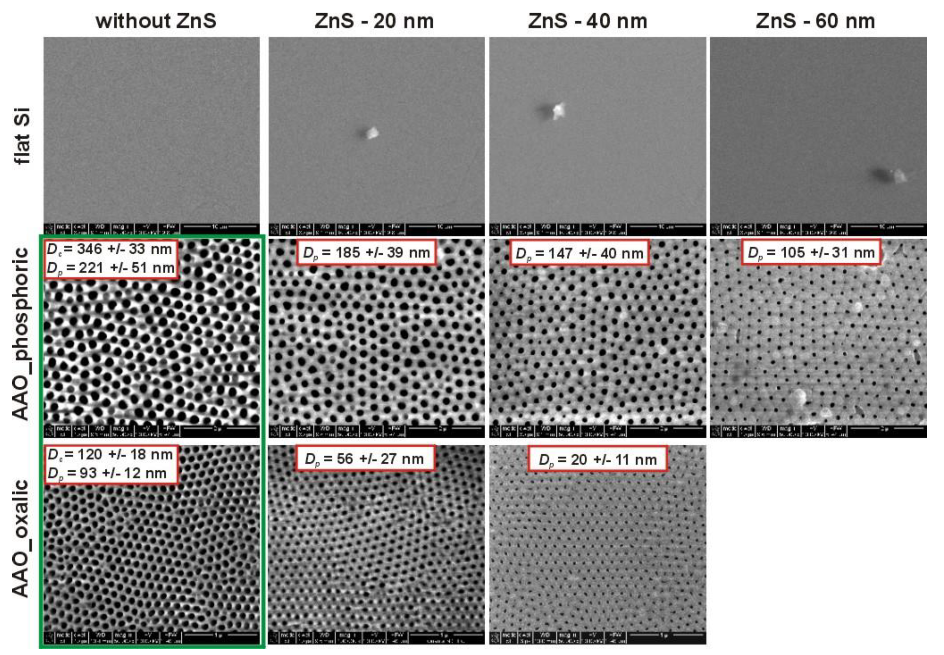
Two groups of samples were analyzed by a standard IR spectroscopy: the Zn–S layers directly after the ALD process (before annealing), and the same samples after annealing. The samples were annealed under argon (99.999%) atmosphere at 400 °C for 1 h. The annealing conditions were chosen based on our previous work [24] to crystallize the amorphous ZnS material. The ZnS layers with the thicknesses of 20, 40, and 60 nm (ZnS–20 nm, ZnS–40 nm, and ZnS–60 nm, respectively) were deposited on flat Si and on porous AAO substrates with an interpore distance (Dc) of ~346 nm (AAO-phosphoric). The 20 and 40 nm thick ZnS layers were also deposited on the porous AAO substrates characterized by about three times smaller Dc ~ 120 nm (AAO-oxalic). The 60-nm thick ZnS thin film was not deposited on the AAO_oxalic because, in this case, the pore diameter was too small (Dp ~ 90 nm) to allow for a uniform coverage of the AAO channels by the Zn–S material. In Figure 1, SEM images of the top view of the samples before annealing are demonstrated. The deposition of ZnS films causes the gradual filling of pores in both AAO_phosphoric and AAO_oxalic porous substrates. As a result, the pore diameter observed in the SEM images decreases with increasing thickness of the ZnS films.
In Figure 2a, an SEM image of a cross-sectional view of the AAO-phosphoric substrate covered with the 60 nm thick Zn–S layer before annealing (AAO_phosphoric-ZnS-60 nm sample), together with EDS elemental mapping images of Al, O, Zn, S, and C (K lines), are presented. The images demonstrate that Zn, S, and C elements are evenly distributed along the entire pore cross-section. After the dissolution of AAO, bundles of ZnS nanotubes were obtained (Figure 2b), which further confirms the homogeneous and complete coverage of the interior of the AAO channels by ZnS material during ALD process. In the EDS spectrum shown in Figure 2c, there are peaks from Zn, S, and C (O and Si elements come from NOA 61 optical adhesive by which the ZnS nanotubes were attached to glass [26]), but no peak from Al was recorded, proving a selective and total dissolution of anodic alumina (in 0.1 M NaOH solution) in the AAO_phosphoric-ZnS-60 nm sample.
In Figure 3, the EDS spectra of the AAO_phosphoric-ZnS-60 nm sample before (a) and after annealing (b) are shown (the spectra were acquired until comparable total number of counts). The spectra demonstrate an apparent increase in Zn lines in the expense of the C line after annealing process. A collective EDS elemental analysis of the AAO_phosphoric-ZnS-20 nm, AAO_phosphoric-ZnS-40 nm, AAO_phosphoric-ZnS-60 nm samples before and after annealing is demonstrated in Figure 3c. The graphs in Figure 3c present the atomic concentration (at.%) of all elements as a function of the ZnS layer thickness. It can be noticed that the concentration of Zn, S, and C elements evidently increases with the increase in the ZnS layer thickness, except the C content in the samples after annealing, which stays on a similar level (~3 at.%). As the amount of all elements adds up to 100% in the EDS analysis, the at.% concentration of all other elements (Al, O, and P; P is present in the AAO matrix due to the incorporation of PO43− ions during anodization in 0.1 M H3PO4 electrolyte [27,28]) tends to decrease with the increase in Zn, S, and C elements. As observed previously [24], before annealing the amount of S is about two times higher than the amount of Zn. The higher amount of S is accompanied by a relatively large amount of C (from ca. 9 to about 14 at.% for the increasing ZnS film thickness) in the samples before annealing. We observed earlier by TOF-ERDA that as-deposited films had a 1:2 Zn:S ratio and 51% C and 27% of H [24]. After annealing, the amount of Zn and S was equalized to similar values and the amount of C dropped significantly to about 3 at.% for all samples. The large amount of carbon, hydrogen and 1:2 Zn:S suggest the presence of unreacted organic precursor in as-deposited film, indicating MLD-type growth of inorganic-organic hybrid materials, while a significant decrease in C in the samples after annealing indicates the removal of the carbon-containing species. Moreover, almost stoichiometric composition of the Zn and S obtained after annealing may indicate the crystallization of the amorphous ZnS material. In order to find out more information about the composition and structure of the ZnS thin films before and after the annealing process, the material was further investigated by XRD, and subsequently by IR spectroscopy.
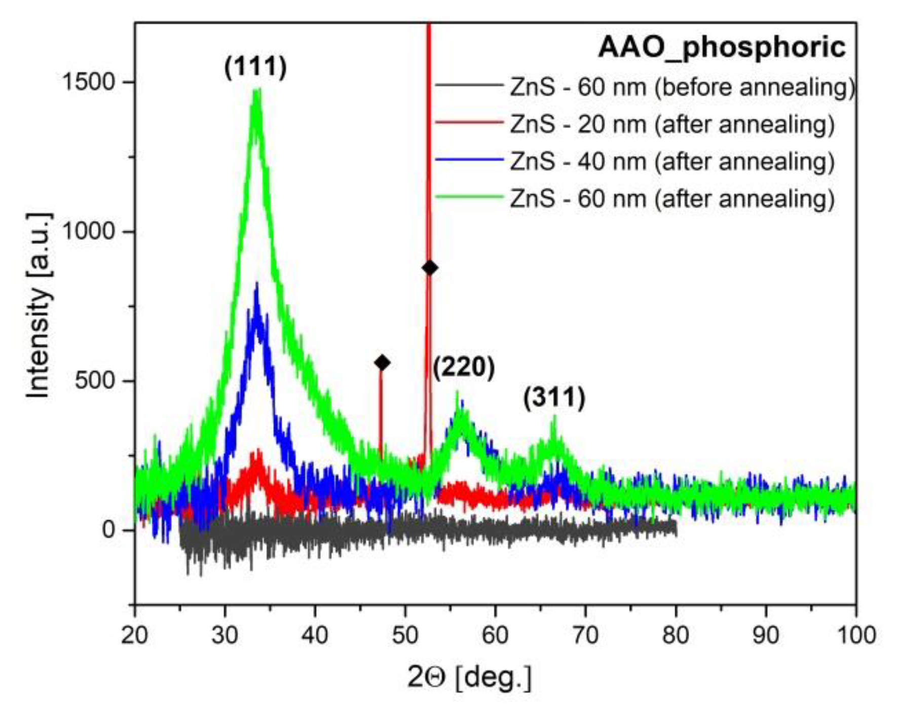
In Figure 4, the XRD patterns of the AAO_phosphoric-ZnS-20 nm, AAO_phosphoric-ZnS-40 nm, AAO_phosphoric-ZnS-60 nm samples after annealing are demonstrated. As shown in the example of the AAO_phosphoric-ZnS-60 nm sample, the ZnS material was amorphous before the annealing process (directly after ALD). After the process, the ZnS crystallizes into cubic form with clearly visible reflections from (111), (220), and (311) crystallographic planes (PDF Number 01-072-4841). The thicker the ZnS film, the more intensive are the peaks in the XRD patterns. A similar transformation of the ZnS material upon heating was observed in the ZnS layer deposited on a flat Si substrate [24]. However, as compared to the XRD profiles of the latter films, the peaks in the Figure 4 are broader. For instance, the FWHM of the (111) reflection is ~6.1° in the XRD pattern of the 60 nm-thick ZnS layer deposited on an AAO_phosphoric porous substrate, while the full width at half maximum (FWHM) of the (111) reflection is around 2.2° in the XRD pattern of the corresponding ZnS layer deposited on the non-porous Si substrate. The peak broadening can be due to smaller crystal size and greater microstrain induced by a porous substrate. In the XRD pattern of the AAO_phosphoric-ZnS-20 nm sample, the lines corresponding to Al are also visible (the AAO was not detached from Al foil after anodization), most probably due to a slightly different sample positioning in the diffractometer and/or larger penetration depth of the X-ray beam, owing to the smaller ZnS film thickness, and thus lower material density.
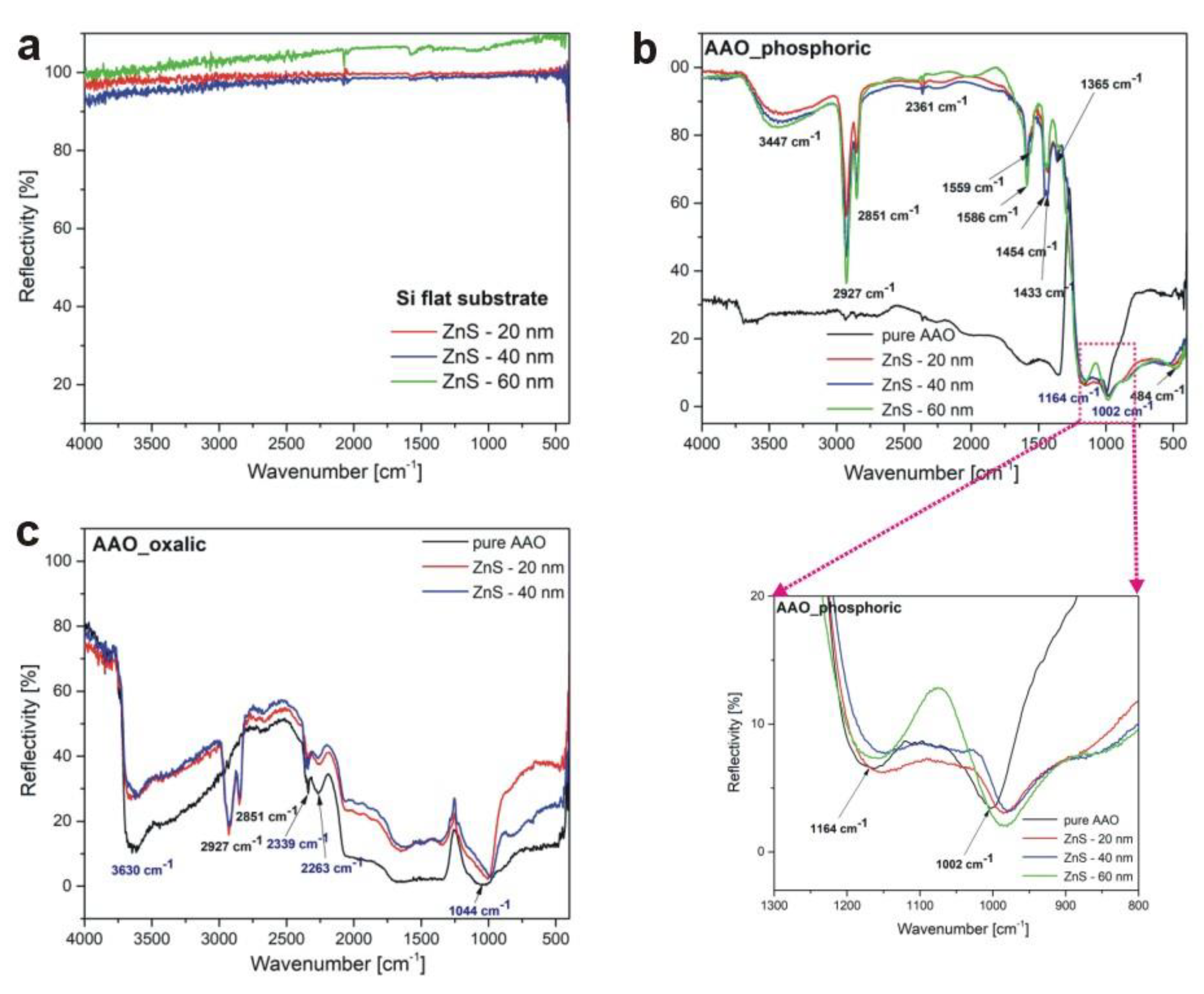
In Figure 5, the IR spectrum of the studied samples are presented. The IR spectra of the amorphous ZnS layers deposited on flat Si substrates display no peaks: the signal was below the detection limit of IR spectroscopy (Figure 5a). In the IR spectra of the same ZnS layers but deposited on porous AAO substrates (Figure 5b,c), distinct absorption peaks are visible, which enable chemical and structural analysis of the layers. A broad vibration centered at ~3450–3650 cm−1, present both in Figure 5b,c, is due to the stretching vibrations of O–H bond (v(OH)) of adsorbed water [29,30,31,32,33]. The vibration confirms the presence of moisture on the surface of ZnS thin films. In the spectral range extending from about 3000 to ca. 1300 cm−1, there are many absorption peaks which cannot originate from chemical groups in the AAO substrate (since they are absent in the IR spectrum of pure AAO in Figure 5b). Zn–S ultrathin films were prepared by low-temperature ALD from diethylzinc (DEZ) and 1,5-pentanedithiol (PDT) as precursors of Zn and S, respectively. Characteristic peaks of IR spectra for 1,5-pentanedithiol can be attributed from each as-deposited Zn–S films on AAO indicating MLD type growth [34,35]. The strongest dips at 2927 and 2851 cm−1 were ascribed before to the CH2 asymmetric (va(CH2)) and symmetric (vs(CH2)) stretching vibrational modes, respectively [29,30,36,37,38]. These dips are also the most intensive ones in the IR spectrum of pure PDT [34,35] and can thus be regarded as chemical fingerprints of this compound. Clearly, with the increase in the thickness of the ZnS layers, the intensity of those two dips increases (Figure 5b). The dips at 1454, 1433 and 1365 cm−1 can be ascribed to the CH or CH2 bending modes [29,30,31,39]. It can be thus concluded that IR analysis provided evidence for the presence of Zn–S-pentanedithiol type MLD hybrid materials, which was already envisaged based on the EDS analysis. Apart from the bands that can be associated with PDT chemical groups, in the IR spectra there are dips that originate from other functional groups. For instance, a weak band at 2361 cm−1 can be attributed to the C=O stretching mode (v3(CO2)) of absorbed CO2 [32,36,40]. The bands at 1559 and 1586 cm−1 were previously associated with C=O stretching vibrations of the absorbed CO2 as well [29,41,42], but could also come from the products of the DEZ and PDT surface reaction. Moreover, there are two dips in the 900–1200 cm−1 spectral range that are also present in the IR spectrum of the pure AAO_phosphoric sample. Both dips are characteristic for phosphonates, which display bands due to the P–O stretching vibration [43,44]. The dip at ~1002 cm−1 can be assigned to the symmetric vibration of the P–O chemical bond (νsP–O) of PO32− group, whereas the one at 1164 cm−1 corresponds most probably to the P=O vibrations. These bands confirm the incorporation of phosphonate ions into the AAO framework during anodization (see the EDS analysis in Figure 3c). After ZnS deposition, the dips tend to shift towards a lower energy (enlarged part of the IR spectra in Figure 5b, marked by dotted magenta frame). A weak and broad band appearing at around 484 cm−1 may originate from the Zn–O stretching vibration [33,36,37,45].
In the ZnS thin films deposited on the AAO_oxalic (Figure 5c), only the bands at 2927 and 2851 cm−1, characteristic for PTD, are clearly visible, while the other bands (at 1454, 1433 and 1365 cm−1) are missing. Moreover, the bands at 2927 and 2851 cm−1 are much weaker in the ZnS film deposited on AAO_oxalic with smaller Dc and Dp parameters as compared to the ones deposited on AAO_phosphoric. Besides, in the IR spectra there are other peaks related to the AAO porous ceramic anodized in oxalic acid solution [46,47]. The bands at 2339 and 2263 cm−1 in pure AAO_oxalic sample may come from v(CH) vibrations of the absorbed hydrogen [48]. The peak at around 1044 cm−1 can be assigned to the coupling of the C–C stretching vibration and the O–C=O bending vibration [49].
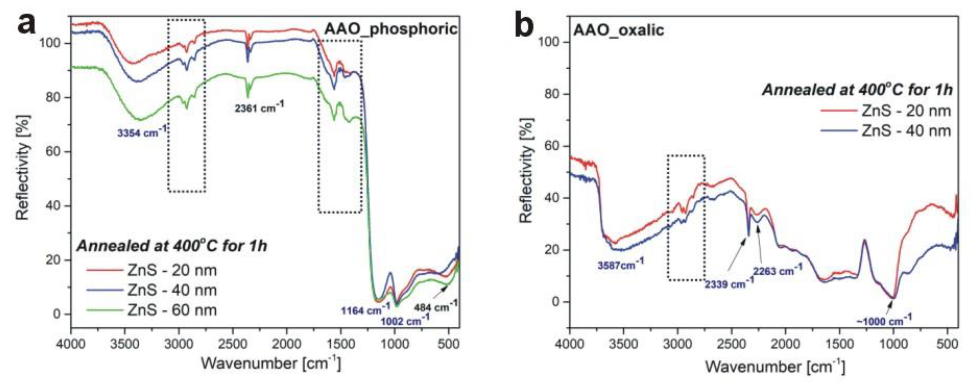
After annealing, the structure of the ZnS films changes substantially (Figure 6). The peaks that were related to the 1,5-pentanedithiol have gone or weakened significantly (dotted, squared frames in Figure 6a,b). On the other hand, the peaks that were ascribed to chemical groups in AAO porous substrates are preserved in the IR spectra. Likewise, a weak and broad peak at around 484 cm−1 that was associated with Zn–O stretching vibration, indicating a partial oxidation of surface Zn. The IR analysis confirmed thus that the low-temperature ALD/MLD process resulted in the synthesis of amorphous Zn–S-1,5-pentanedithiol hybrid materials. Heating of the layers at 400 °C for 1h is sufficient to improve the composition and structure of ZnS. The analysis of the same ZnS layers deposited on flat Si substrate was not possible by a standard IR spectroscopy due to the constraints related to small layer thickness. Long and parallel channels of anodic alumina (AAO), uniformly covered by the ZnS thin films, enhanced the effective optical path length and the interaction of the ZnS film with incident IR light, thus enabling a reliable chemical analysis of the ZnS layers as thin as 20 nm.
4. Conclusions
In this work, it was demonstrated that ultrathin films (20–60 nm) can be successfully investigated by standard IR spectroscopy when deposited on porous substrates with a well-developed surface area. As an example, hybrid Zn–S-1,5-pentanedithiol and ZnS thin films were analyzed which were deposited on flat Si and porous AAO substrates. In contrast to the films deposited on the porous AAO substrates, the same films on a flat Si substrate could not be analyzed by IR spectroscopy: in the IR spectrum, no bands were detected. Thanks to the application of the AAO porous support, it was possible to study the structure and composition of the Zn–S-1,5-pentanedithiol and ZnS ultrathin films synthesized by ALD/MLD from diethylzinc (DEZ) and 1,5-pentanedithiol (PDT) as precursors of Zn and S, respectively. According to IR analysis, it was revealed that the low temperature ALD deposition of 150 °C resulted in the production of amorphous hybrid material with 1,5-pentanethiol. Moreover, it was observed that the signal-to-noise ratio increases as the thickness of the Zn–S layer increases, and as the diameter of the AAO channels and interpore distance increase. After annealing at 400 °C for 1 h, the amorphous films transformed into cubic ZnS form, which was also indicated in the IR spectra: the bands related to the unreacted precursors disappeared or weakened substantially. The approach presented in this study can be applied to study any ultrathin films, where the porous ceramic support can serve as a reference substrate for the film to be studied by a standard IR spectroscopy.
Author Contributions
Conceptualization, M.N.; methodology, M.P.; investigation, M.W. and M.P.; measurements, M.W. and M.N.; writing—original draft preparation, M.N.; writing—review and editing, M.P.; All authors have read and agreed to the published version of the manuscript.
Funding
The work was supported by the statutory research funds of the Department of Functional Materials and Hydrogen Technology, Military University of Technology, Warsaw, Poland. M.P. acknowledges funding from the Academy of Finland by the profiling action on Matter and Materials, Grant No. 318913.
Conflicts of Interest
The authors declare no conflict of interest.
References
- Wetzig, K.; Schneider, C.M. Metal Based Thin Films for Electronics, 2nd ed.; Wiley-VCH Verlag GmbH & Co. KGaA: Weinheim, Germany, 2006. [Google Scholar]
- Piegari, A.; Flory, F. Optical Thin Films and Coatings: From Materials to Applications, 2nd ed.; Woodhead Publishing: Cambridge, UK, 2018. [Google Scholar]
- Grandin, G.M.; Textor, M. Intelligent Surfaces in Biotechnology: Scientific and Engineering Concepts, Enabling Technologies, and Translation to Bio-Oriented Applications; John Wiley & Sons, Inc.: Hoboken, NJ, USA, 2012. [Google Scholar]
- Johnson, R.W.; Hultqvist, A.; Bent, S.F. A brief review of atomic layer deposition: From fundamentals to applications. Mater. Today 2014, 17, 236–246. [Google Scholar] [CrossRef]
- Knez, M.; Nielsch, K.; Niinisto, L. Synthesis and Surface Engineering of Complex Nanostructures by Atomic Layer Deposition. Adv. Mater. 2007, 19, 3425–3438. [Google Scholar] [CrossRef]
- Wang, K.X.; Yu, Z.; Liu, V.; Cui, Y.; Fan, S. Absorption Enhancement in Ultrathin Crystalline Silicon Solar Cells with Antireflection and Light-Trapping Nanocone Gratings. Nano Lett. 2012, 12, 1616–1619. [Google Scholar] [CrossRef] [PubMed] [Green Version]
- Islam, R.; Saraswat, K. Limitation of Optical Enhancement in Ultra-thin Solar Cells Imposed by Contact Selectivity. Sci. Rep. 2018, 8, 8863. [Google Scholar] [CrossRef] [PubMed]
- Tchoe, Y.; Chung, K.; Lee, K.; Jo, J.; Chung, K.; Hyun, J.K.; Kim, M.; Yi, G.-C. Free-standing and ultrathin inorganic light-emitting diode array. NPG Asia Mater. 2019, 11, 377. [Google Scholar] [CrossRef] [Green Version]
- Youngquist, R.C.; Nurge, M.A.; Fisher, B.H.; Malocha, D.C. A Resistivity Model for Ultrathin Films and Sensors. IEEE Sens. J. 2014, 15, 2412–2418. [Google Scholar] [CrossRef]
- Sundberg, P.; Karppinen, M. Organic and inorganic–organic thin film structures by molecular layer deposition: A review. Beilstein J. Nanotechnol. 2014, 5, 1104–1136. [Google Scholar] [CrossRef]
- Zhao, J.; Bradbury, C.R.; Huclova, S.; Potapova, I.; Carrara, M.; Fermin, D.J. Nanoparticle-Mediated Electron Transfer Across Ultrathin Self-Assembled Films. J. Phys. Chem. B 2005, 109, 22985–22994. [Google Scholar] [CrossRef]
- Tang, C.; Yan, Z.; Wang, Q.; Chen, J.; Zhu, M.; Liu, B.; Liu, F.; Sui, C. Ultrathin amorphous silicon thin-film solar cells by magnetic plasmonic metamaterial absorbers. RSC Adv. 2015, 5, 81866–81874. [Google Scholar] [CrossRef]
- Koh, Y.P.; McKenna, G.B.; Simon, S.L. Calorimetric glass transition temperature and absolute heat capacity of polystyrene ultrathin films. J. Polym. Sci. Part B Polym. Phys. 2006, 44, 3518–3527. [Google Scholar] [CrossRef]
- Harada, K.; Sugimoto, T.; Kato, F.; Watanabe, K.; Matsumoto, Y. Thickness dependent homogeneous crystallization of ultrathin amorphous solid water films. Phys. Chem. Chem. Phys. 2020, 22, 1963–1973. [Google Scholar] [CrossRef] [PubMed]
- Yang, W.; Zhao, Z.; Wu, K.; Huang, R.; Liu, T.; Jiang, H.; Chen, F.; Fu, Q. Ultrathin flexible reduced graphene oxide/cellulose nanofiber composite films with strongly anisotropic thermal conductivity and efficient electromagnetic interference shielding. J. Mater. Chem. C 2017, 5, 3748–3756. [Google Scholar] [CrossRef]
- Hoffmann, F.M.; Levinos, N.J.; Perry, B.N.; Rabinowitz, P. High-resolution infrared reflection absorption spectroscopy with a continuously tunable infrared laser: CO on Ru(001). Phys. Rev. B 1986, 33, 4309–4311. [Google Scholar] [CrossRef] [PubMed]
- Jiang, E.Y. Advanced FT-IR Spectroscopy; Thermo Electron Corporation: Madison, WI, USA, 2003; p. 58. [Google Scholar]
- Wang, C.; Zheng, J.; Zhao, L.; Rastogi, V.K.; Shah, S.S.; DeFrank, J.J.; Leblanc, R.M. Infrared reflection-absorption spectroscopy and polarization-modulated infrared reflection-absorption spectroscopy studies of the organophoshorus aicd anhydrolase langmuir monolayer. J. Phys. Chem. B 2008, 112, 5250–5256. [Google Scholar] [CrossRef] [PubMed]
- Monyoncho, E.; Zamlynny, V.; Woo, T.K.; Baranova, E.A. The utility of polarization modulation infrared reflection absorption spectroscopy (PM-IRRAS) in surface and in situ studies: New data processing and presentation approach. Analytics 2018, 143, 2563–2573. [Google Scholar] [CrossRef]
- Baldassarre, M.; Barth, A. Pushing the detection limit of infrared spectroscopy for structural analysis of dilute protein samples. Analytics 2014, 139, 5393–5399. [Google Scholar] [CrossRef]
- Andersen, A.; Yamada, S.; Pramodkumar, E.; Andresen, T.L.; Boisen, A.; Schmid, S. Nanomechanical IR spectroscopy for fast analysis of liquid-dispersed engineered nanomaterials. Sensors Actuators B Chem. 2016, 233, 667–673. [Google Scholar] [CrossRef] [Green Version]
- Larsen, T.; Schmid, S.; Villanueva, L.G.; Boisen, A. Photothermal Analysis of Individual Nanoparticulate Samples Using Micromechanical Resonators. ACS Nano 2013, 7, 6188–6193. [Google Scholar] [CrossRef]
- Ko, D.; Kim, S.; Jin, Z.; Shin, S.; Lee, S.Y.; Min, Y.-S. A Novel Chemical Route to Atomic Layer Deposition of ZnS Thin Film from Diethylzinc and 1,5-Pentanedithiol. Bull. Korean Chem. Soc. 2017, 38, 696–699. [Google Scholar] [CrossRef]
- Włodarski, M.; Chodorow, U.; Jóźwiak, S.; Putkonen, M.; Durejko, T.; Sajavaara, T.; Norek, M. Structural and Optical Characterization of ZnS Ultrathin Films Prepared by Low-Temperature ALD from Diethylzinc and 1.5-Pentanedithiol after Various Annealing Treatments. Materials 2019, 12, 3212. [Google Scholar] [CrossRef] [Green Version]
- Horcas, I.; Fernández, R.; Gomez-Rodriguez, J.M.; Colchero, J.W.; Gómez-Herrero, J.W.; Baro, A.M. WSXM: A software for scanning probe microscopy and a tool for nanotechnology. Rev. Sci. Instruments 2007, 78, 13705. [Google Scholar] [CrossRef] [PubMed]
- Harding, D.R.; Goodrich, H.; Caveglia, A.; Anthamatten, M. Effect of temperature and volume on the tensile and adhesive properties of photocurable resins. J. Polym. Sci. Part B Polym. Phys. 2014, 52, 936–945. [Google Scholar] [CrossRef]
- Ofoegbu, S.U.; Fernandes, F.A.O.; Pereira, A.B. The Sealing Step in Aluminum Anodizing: A Focus on Sustainable Strategies for Enhancing Both Energy Efficiency and Corrosion Resistance. Coatings 2020, 10, 226. [Google Scholar] [CrossRef] [Green Version]
- Xu, Y.; Thompson, G.; Wood, G.; Bethune, B. Anion incorporation and migration during barrier film formation on aluminium. Corros. Sci. 1987, 27, 83–102. [Google Scholar] [CrossRef]
- Qu, H.; Cao, L.; Su, G.; Liu, W.; Gao, R.; Xia, C.; Qin, J. Silica-coated ZnS quantum dots as fluorescent probes for the sensitive detection of Pb2+ ions. J. Nanoparticle Res. 2014, 16, 2762. [Google Scholar] [CrossRef]
- Kharazmi, A.; Faraji, N.; Hussin, R.M.; Saion, E.; Yunus, W.M.M.; Behzad, K. Structural, optical, opto-thermal and thermal properties of ZnS–PVA nanofluids synthesized through a radiolytic approach. Beilstein J. Nanotechnol. 2015, 6, 529–536. [Google Scholar] [CrossRef] [Green Version]
- Xaba, T.; Moloto, M.J.; Al-Shakban, M.; Malik, M.A.; O’Brien, P.; Moloto, M.J. The influences of the concentrations of “green capping agents” as stabilizers and of ammonia as an activator in the synthesis of ZnS nanoparticles and their polymer nanocomposites. Green Process. Synth. 2017, 6, 173–182. [Google Scholar] [CrossRef]
- Shanmugam, N.; Cholan, S.; Viruthagiri, G.; Gobi, R.; Kannadasan, N. Synthesis and characterization of Ce3+-doped flowerlike ZnS nanorods. Appl. Nanosci. 2013, 4, 359–365. [Google Scholar] [CrossRef] [Green Version]
- Estévez-Hernández, O.; Hernandez, M.P.P.; Farías, M.H.; Rodríguez-Hernández, J.; Gonzalez, M.M.; Reguera, E. Effect of Co-Doping on the Structural, Electronic and Magnetic Properties of CoxZn1–xO Nanoparticles. Mater. Focus 2017, 6, 371–381. [Google Scholar] [CrossRef]
- ChemicalBook. Available online: https://www.chemicalbook.com/SpectrumEN_928-98-3_IR1.htm (accessed on 12 January 2020).
- Öztürk, N.; Çırak, Ç.; Bahçeli, S. FT-IR Spectroscopic Study of 1,5-Pentanedithiol and 1,6-Hexanedithiol Adsorbed on NaA, CaA and NaY Zeolites. Zeitschrift für Naturforschung A 2014, 60, 633–636. [Google Scholar] [CrossRef]
- Segala, K.; Dutra, R.L.; Franco, C.V.; Pereira, A.S.; Trindade, T. In Situ and Ex Situ Preparations of ZnO/Poly-{trans-[RuCl2(vpy)4]/styrene} Nanocomposites. J. Braz. Chem. Soc. 2010, 21, 1986–1991. [Google Scholar] [CrossRef] [Green Version]
- Hosseini, S.A.; Mashaykhi, S.; Babaei, S. Graphene oxide/zinc oxide nanocomposite: A superior adsorbent for removal of methylene blue—Statistical analysis by response surface methodology (RSM). South Afr. J. Chem. 2016, 69, 105–112. [Google Scholar] [CrossRef]
- Gärd, R.; Sun, Z.-X.; Forsling, W. FT-IR and FT-Raman Studies of Colloidal ZnS. J. Colloid Interface Sci. 1995, 169, 393–399. [Google Scholar] [CrossRef]
- Thottoli, A.K.; Achuthanunni, A.K. Effect of polyvinyl alcohol concentration on the ZnS nanoparticles and wet chemical synthesis of wurtzite ZnS nanoparticles. J. Nanostructure Chem. 2013, 3, 31. [Google Scholar] [CrossRef] [Green Version]
- Pandey, B.K.; Sukla, A.; Sinha, A.K.; Gopal, R. Synthesis and Characterization of Cobalt Oxalate Nanomaterial for Li-Ion Battery. Mater. Focus 2015, 4, 333–337. [Google Scholar] [CrossRef]
- Mote, V.D.; Purushotham, Y.; Dole, B.N. Structural, morphological and optical properties of Mn doped ZnS nanocrystals. Cerâmica 2013, 59, 614–619. [Google Scholar] [CrossRef] [Green Version]
- Chen, Y.; Kim, M.; Lian, G.; Johnson, M.B.; Peng, X. Side Reactions in Controlling the Quality, Yield, and Stability of High Quality Colloidal Nanocrystals. J. Am. Chem. Soc. 2005, 127, 13331–13337. [Google Scholar] [CrossRef]
- Zenobi, M.C.; Luengo, C.; Avena, M.J.; Rueda, E.H. An ATR-FTIR study of different phosphonic acids in aqueous solution. Spectrochim. Acta Part A Mol. Biomol. Spectrosc. 2008, 70, 270–276. [Google Scholar] [CrossRef]
- Gong, W. A real time in situ ATR-FTIR spectroscopic study of linear phosphate adsorption on titania surfaces. Int. J. Miner. Process. 2001, 63, 147–165. [Google Scholar] [CrossRef]
- Wang, L.; Wu, Y.; Chen, F.; Yang, X. Photocatalytic enhancement of Mg-doped ZnO nanocrystals hybridized with reduced graphene oxide sheets. Prog. Nat. Sci. 2014, 24, 6–12. [Google Scholar] [CrossRef] [Green Version]
- Onija, O.; Borodi, G.; Kacso, I.; Pop, M.N.; Dadarlat, D.; Bratu, I.; Jumate, N.; Lazar, M.D. Preparation and characterization of urea-oxalic acid solid form. Process. Isotopes Mol. PIM 2012, 35, 35–38. [Google Scholar] [CrossRef]
- Pan, Y.-T.; Wang, D.-Y. Fabrication of low-fire-hazard flexible poly (vinyl chloride) via reutilization of heavy metal biosorbents. J. Hazard. Mater. 2017, 339, 143–153. [Google Scholar] [CrossRef] [PubMed]
- Varghese, M.; Jochan, J.; Sabu, J.; Varughese, P.A.; Abraham, K.E. Spectral properties of cadmium malonate crystals grown in hydrosilica gel. Ind. J. Pure Appl. Phys. 2009, 47, 691–695. [Google Scholar]
- de Azevedo, W.M.; de Oliveira, G.B.; da Silva, E.F., Jr.; Khoury, H.J.; Oliveira de Jesus, E.F. Highly sensitive thermoluminescent carbon doped nanoporous aluminum oxide detectors. Radiat. Protect. Dosimet. 2006, 119, 201–205. [Google Scholar] [CrossRef] [PubMed]
Figure 1.
SEM images of the ZnS layers with a thickness of 20, 40, and 60 nm deposited on flat Si substrates (first row; scale bar = 10 μm), porous anodic alumina (AAO) substrates with Dc ~ 346 nm (second row; scale bar = 2 μm), and the porous AAO substrates with Dc ~ 120 nm (third row, scale bar = 1 μm).

Figure 2.
SE image of a cross-sectional view of the AAO_phosphoric-ZnS-60 nm sample before annealing, and corresponding EDS elemental mapping of Al, O, Zn, S, and C (scale bar = 2 μm) (a); SEM image of the ZnS nanotubes after dissolution of AAO in the AAO_phosphoric-ZnS-60 nm sample (b) and corresponding EDS spectrum (c).

Figure 3.
EDS spectrum of the AAO_phosphoric-ZnS-60 nm sample before (a) and after annealing (b); EDS elemental analysis of the samples AAO_phosphoric-ZnS-20 nm, AAO_phosphoric-ZnS-40 nm, AAO_phosphoric-ZnS-60 nm before and after annealing (c).
Figure 3.
EDS spectrum of the AAO_phosphoric-ZnS-60 nm sample before (a) and after annealing (b); EDS elemental analysis of the samples AAO_phosphoric-ZnS-20 nm, AAO_phosphoric-ZnS-40 nm, AAO_phosphoric-ZnS-60 nm before and after annealing (c).

Figure 4.
XRD patterns of the AAO_phosphoric-ZnS-60 nm sample before annealing and the samples AAO_phosphoric-ZnS-20 nm, AAO_phosphoric-ZnS-40 nm, AAO_phosphoric-ZnS-60 nm after annealing (the black diamond symbols signify the reflections originating from the Al substrate).
Figure 4.
XRD patterns of the AAO_phosphoric-ZnS-60 nm sample before annealing and the samples AAO_phosphoric-ZnS-20 nm, AAO_phosphoric-ZnS-40 nm, AAO_phosphoric-ZnS-60 nm after annealing (the black diamond symbols signify the reflections originating from the Al substrate).

Figure 5.
IR spectrum of the Zn–S-1,5-pentanedithiol layers deposited on flat Si substrate (a) and on AAO_phosphoric (b) and AAO_oxalic (c) porous substrates before annealing process.
Figure 5.
IR spectrum of the Zn–S-1,5-pentanedithiol layers deposited on flat Si substrate (a) and on AAO_phosphoric (b) and AAO_oxalic (c) porous substrates before annealing process.

Figure 6.
IR spectrum of the ZnS layers deposited on AAO_phosphoric (a) and AAO_oxalic (b) porous substrates after annealing at 400 °C for 1 h.
Figure 6.
IR spectrum of the ZnS layers deposited on AAO_phosphoric (a) and AAO_oxalic (b) porous substrates after annealing at 400 °C for 1 h.

© 2020 by the authors. Licensee MDPI, Basel, Switzerland. This article is an open access article distributed under the terms and conditions of the Creative Commons Attribution (CC BY) license (http://creativecommons.org/licenses/by/4.0/).
Share and Cite
MDPI and ACS Style
Włodarski, M.; Putkonen, M.; Norek, M. Infrared Absorption Study of Zn–S Hybrid and ZnS Ultrathin Films Deposited on Porous AAO Ceramic Support. Coatings 2020, 10, 459. https://doi.org/10.3390/coatings10050459
AMA Style
Włodarski M, Putkonen M, Norek M. Infrared Absorption Study of Zn–S Hybrid and ZnS Ultrathin Films Deposited on Porous AAO Ceramic Support. Coatings. 2020; 10(5):459. https://doi.org/10.3390/coatings10050459
Chicago/Turabian StyleWłodarski, Maksymilian, Matti Putkonen, and Małgorzata Norek. 2020. "Infrared Absorption Study of Zn–S Hybrid and ZnS Ultrathin Films Deposited on Porous AAO Ceramic Support" Coatings 10, no. 5: 459. https://doi.org/10.3390/coatings10050459
Note that from the first issue of 2016, this journal uses article numbers instead of page numbers. See further details here.