Article

Optimization of Ultra-Thin Pulsed-DC Magnetron Sputtered Aluminum Films for the Technology of Hyperbolic Metamaterials

1
Institute of Microelectronics and Optoelectronics, Warsaw University of Technology, Koszykowa 75, 00-662 Warsaw, Poland
2
Institute of Physics, Polish Academy of Sciences, Al. Lotników 32/46, 02-668 Warsaw, Poland
3
Faculty of Physics, Warsaw University of Technology, Koszykowa 75, 00-662 Warsaw, Poland
*
Author to whom correspondence should be addressed.
Crystals 2020, 10(5), 384; https://doi.org/10.3390/cryst10050384
Submission received: 8 April 2020 / Revised: 5 May 2020 / Accepted: 7 May 2020 / Published: 8 May 2020
(This article belongs to the Special Issue Metamaterials)

Abstract

:
The future applications of hyperbolic metamaterials demand stacks of materials with alternative ultra-thin conductive/dielectric films with good homogeneity of the thickness and reduced roughness level. In this work, the technology of pulsed-DC magnetron sputtering of aluminum was optimized using the Taguchi method in order to fabricate Al films with improved roughness level. The performed structural characterization proved the smaller Al domains and better homogeneity of the surface. The optimized process was used to fabricate a multilayer structure of Al/HfOx as the metamaterial media. The fabricated structures were optically characterized in the UV/VIS range. The presented findings demonstrated the tunability effect of the effective reflectance of the examined stacks. The presented results are promising for the future application of multilayer structures in novel photonic devices based on hyperbolic metamaterials.

1. Introduction

Conductive materials fabricated from aluminum films are commonly used in current semiconductor technologies in the form of connections or inter-metal dielectric layers [1,2]. Aluminum films also find numerous applications in optoelectronics and photovoltaics as anti- or reflective coatings and lateral current collective materials [3,4]. While inhomogeneities of thickness are of little importance in these applications, the modern technologies of nanoelectronic and photonic devices demand the fabrication of conductive films in the thin, and ultra-thin regime (up to 20 nm). The roughness of such films is becoming increasingly important, as it influences the optical properties and integrity of multi-layer structures which are the basis for the fabrication of novel nano-engineered media known as metamaterials, i.e., materials with a negative refractive index called left-handed [5,6].
These kinds of materials offer unique electromagnetic responses that can be obtained neither in conventional media nor in nature. The specific class of metamaterials, which became particularly important at THz, as well as mid-infrared (MIR), near-infrared (NIR), and optical frequencies, are hyperbolic metamaterials (HMMs) [7]. Such structures are typically composed of periodically arranged metallic/dielectric sub-wavelength planar bilayers. These structures are commonly known in the literature as 1D-HMM since its spatial periodicity is observed in a single (1D) direction.
The most striking feature of HMMs that comes from the hyperboloidal shape of their iso-frequency contour in the k-wavevector space is the existence of unique states with large magnitude wavevectors (the high-k states), which decay exponentially in conventional media [8]. This feature gives rise to many device applications ranging from imaging to quantum nanophotonics [9], obtaining broadband Purcell effect [10] or controlling spontaneous emission rate of emitters [11,12]. Moreover, HMM-based waveguides offer unusual properties including the absence of fundamental modes, double degeneracy of the modes, the sign-varying energy flux [13], as well as slowing down the speed of light, enabling possible applications as optical buffers and delay lines in integrated optical circuits [14]. Recent studies have shown the possibility of tuning their optical properties in THz, infrared, and optical frequency ranges by applying an external electric field [15,16,17].
This study presents optimization results of thickness inhomogeneity of aluminum films fabricated through pulsed-DC magnetron sputtering process for the application in multilayer structures that are the basis for the hyperbolic metamaterials. In this work, the experimental runs were designed according to the Design of Experiments (DoE) method, namely Taguchi orthogonal tables [18]. DoE is a methodology for systematically applying statistics to experimentation [19]. It can be also defined as a series of tests in which purposeful changes are made to the input variables of a process or system so that the reasons for these changes in the output response may be observed and identified [20]. Numerous case studies in different areas of application prove the advantages and potential of DoE methods, such as Block Designs, Two-Level/General/Fractional Factorial Experiments, Response Surface Methodology, or Evolutionary Algorithms [21,22,23]. However, the use of orthogonal tables employing the Taguchi approach is easy to implement and quite effective, allows for a large saving in an experimental effort, and is simple to analyze. Therefore, orthogonal tables have already found number of implementations in environmental [24], and agricultural sciences [25], physics [26], chemistry [27], statistics [28], management and business [29], or medicine [30].
The DoE method used in this study allowed for the investigations of dependencies between variables of process’ parameters, i.e., magnetron sputtering, and output parameters, i.e., the properties of the examined material [31]. Within this work, the effective optimization of the homogeneity of aluminum films was performed. As a consequence of the optimization process, the set of variables of the magnetron sputtering process was designed resulting in the Al film with the controllable thickness and smooth surface. This finding allowed for the successful fabrication of multilayer structures based on Al and hafnium oxide (HfOx) ultra-thin films. Finally, we present the preliminary experimental results of the tunability of Al/HfOx stacks that might have found the practical application in photonic structures based on HMMs [32,33,34].

2. Materials and Methods

In this study, aluminum and hafnium oxide films were fabricated using a pulsed-DC magnetron sputtering method using a PlasmaLab System 400 made by Oxford Instruments Plasma Technology (Yatton, Bristol, UK). All processing steps were performed at room temperature using the 8-inch Al and Hf targets with 99.999% purity level. While the aluminum films were deposited in argon (Ar) atmosphere, the hafnium oxide films were formed in reactive mode with argon and oxygen-based plasma. The substrates were positioned on-axis of the sputtering beam and the target-to-substrate distance was of the order of 20 cm. Before the fabrication of conductive and dielectric films, Si substrates were cleaned by means of modified Radio Corporation of America (RCA) method (piranha + SC1 + SC2 + BHF dipping). A three-stage optimization procedure was performed to achieve satisfying results and a significant decrease in the roughness of investigated Al films. During the optimization, all processing steps of the fabrication of Al films were conducted on silicon substrates, as they are characterized by a perfect smoothness level. Thus, during the optimization procedure, all inhomogeneities of the aluminum thickness appeared after the fabrication of conductive film and must originate from the deposition process conditions.
The first stage was aimed to investigate the influence of sputtering process’ parameters on the kinetics growth and roughness of aluminum films. The set of input (process’) parameters was designed using L9(43) and L25(45) orthogonal tables. These orthogonal tables assume the investigation of the influence of four process parameters, each with three or five variables, respectively, onto the output properties. The number of processing steps was 9 and 25, respectively. The aim of the use of the L25(45) table was to compare the obtained trends between two different designs of the experimental runs and to prove the correctness of the obtained trends with the use of a higher number of processes. The influence of pressure in the reactive chamber, power applied to the electrodes, argon flow, and time of the sputtering on the thickness and roughness of fabricated films were considered in this study. Table 1 and Table 2 present the selected values of the process’ parameters for the optimization of aluminum thin films within both examined experimental designs.
The obtained results allowed for the selection of the most promising parameters to obtain the conductive layer with tailored properties, i.e., a good homogeneity of the surface and controllable thickness. Thus, in the second stage of the experimental part, the verification of the optimization procedure was carried out and the two sets of sputtering parameters were designed in order to form a conductive material, i.e., (1) with the possible best, and (2) the worst roughness level. This procedure was aimed to show that the optimization using the Taguchi approach was performed successfully and the fabrication of conductive film is controllable.
In the third stage, the multilayer structures were fabricated using the optimized process of Al sputtering. The fabricated stacks were composed of alternating layers of hafnium oxide and aluminum films. In the end, the optical properties of obtained films were examined and the possibility to tune the optical properties of examined stacks was demonstrated.
The thickness and structural properties of investigated Al films were characterized using spectroscopic ellipsometry, Atomic Force Microscopy (AFM), Scanning Electron Microscopy (SEM), and High-Resolution Transmission Electron Microscopy (HR-TEM). The thickness of investigated aluminum thin films was determined using Horiba Jobin-Yvon UVISEL spectroscopic ellipsometer (Glasgow, UK), in a wavelength range from 190 nm to 850 nm. The ellipsometry was also used to characterize the optical properties of Al/HfOx stacks. The surface homogeneity and morphology characterization were done using the Bruker Dimension Icon microscope (Coventry, UK), in tapping mode using additionally ScanAsyst algorithm. It allows automatic optimization of scan parameters (e.g., gain) during scanning, which results in an ultra-low noise level. The apparatus ensure quantitative and qualitative atomic force measurements with a resolution of the order of 0.03 nm in Z-direction and 0.15 nm in X,Y-direction. The images of areas sized 1 μm × 1 μm or 10 μm × 10 μm were collected to evaluate the topography of examined materials and calculate their roughness as root-mean-square (RMS) values. The RMS noise in the vertical dimension was equal to 0.03 nm. The samples for the HR-TEM examinations were prepared using a Focused Ion Beam (FIB) device (NB5000 Hitachi) (Mannheim, Germany), and ultimate structuring was performed using a Linda GenteMill low-voltage ion thinner. During FIB preparation, a thin layer of carbon was evaporated employing electron-gun sputtering, followed by tungsten evaporation using a gallium ions source. Ion milling was carried out on both sides of the samples at 0.5 kV. Then, the samples were analyzed using a Hitachi HD2700 HR-TEM (Mannheim, Germany). The investigated samples were analyzed using the bright-field STEM (BF-STEM) mode, where diffraction contrast is dominant, and the high-angle annular dark-field STEM (HAADF-STEM) mode, where mass contrast is dominant.

3. Results and Discussion

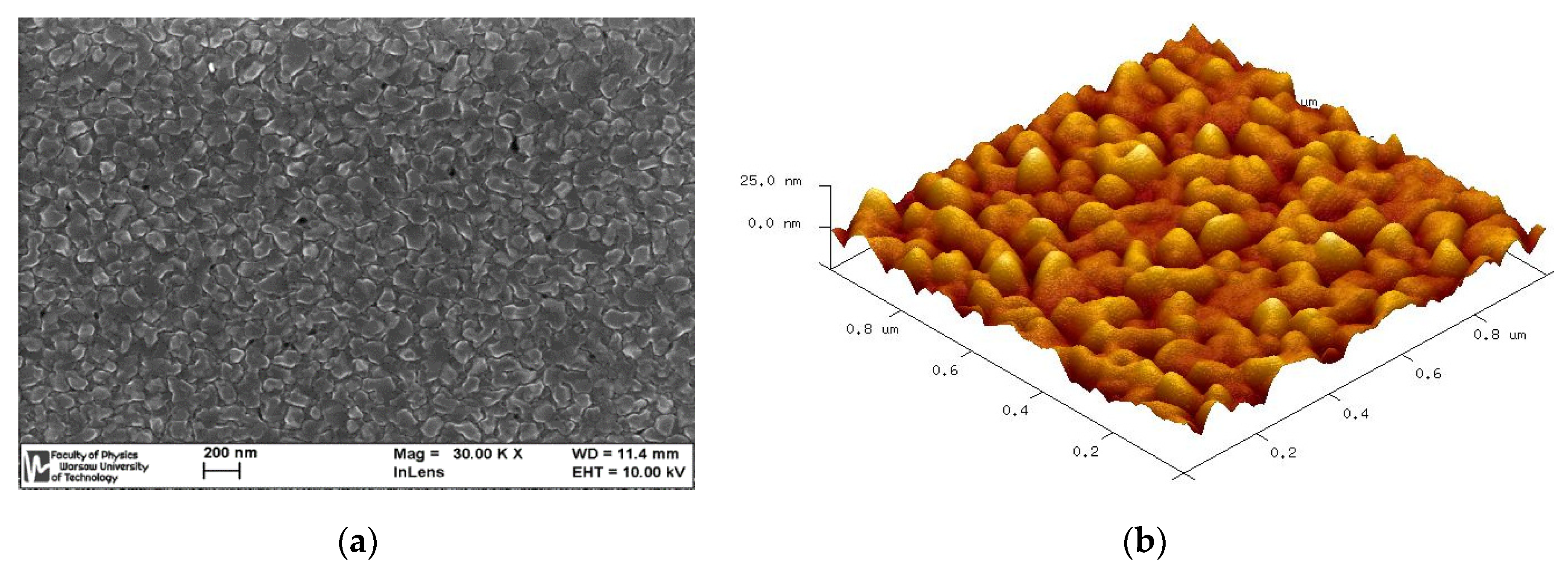
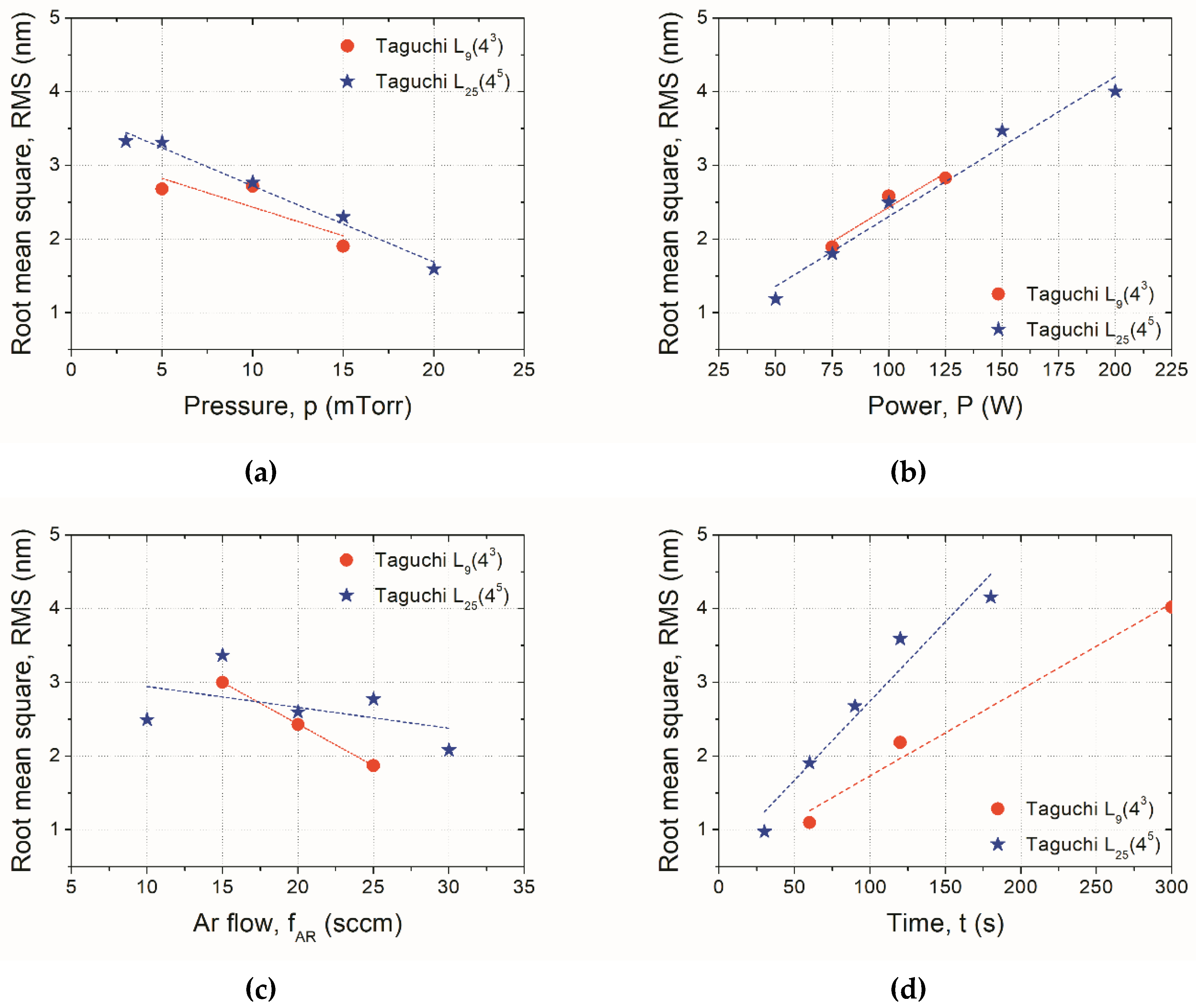
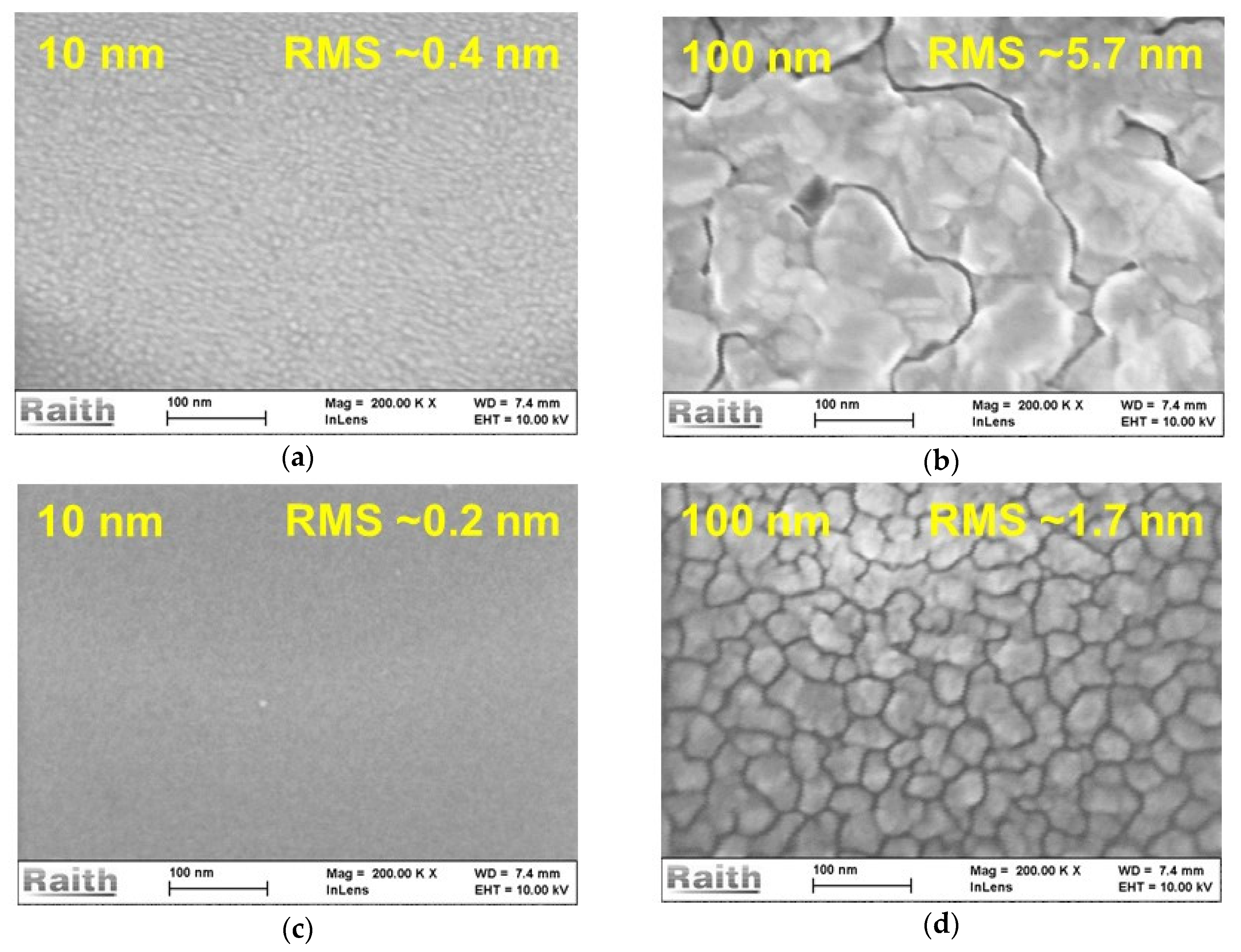
3.1. Investigations of the Influence of Sputtering Process’ Parameters onto the Kinetic Growth and Homogeneity of Aluminum Films

It is commonly known that the typical sputtered aluminum films can be characterized by inhomogeneity of thickness and a high level of surface roughness [35]. The AFM and SEM micrographs presented in Figure 1 show topography of 30 nm Al film formed by magnetron sputtering. It is visible that a conductive material is characterized by a high degree of polycrystalline and a multi-domain structure. The estimated RMS factor is of the order of 6.2 nm. The surface roughness limits the fabrication of structures based on thin and ultra-thin multilayers as the formation of consecutive layers results in duplication and enlargement of the heterogeneity of the initial topography and significantly multiplies errors of the ultimate surface.
The cross-section of Al/HfOx stack obtained by the TEM method is presented in Figure 2. The presented stack was fabricated as the example and comparison of the structure’s homogeneity and composition of two different materials, i.e., dielectric, and conductive one. It is worth noting the high level of roughness of Al film on top of very homogenous and smooth ultra-thin hafnium oxide dielectric film. The presented micrograph proves that it is almost impossible to determine the location of the interface between bulk material and a surface.
In the first stage of optimization, to limit the roughness of Al films the influence of the input process’ parameters on output parameters (i.e., RMS factor of obtained conductive films) was analyzed. It allowed for the selection of the most promising values of sputtering to fabricate the Al films with the possibly low surface roughness. The influence of the sputtering’s parameters onto the RMS factor of conductive material is depicted in Figure 3. The results presented in Figure 3 were shown according to the analysis of data in the DoE method and depict the comparison of obtained trends from both examined experimental designs.
The data presented in Figure 3 indicates that all parameters of the sputtering process have a reasonable effect on the roughness of aluminum films; however, the power applied to the electrodes is the most influential on the ultimate homogeneity of Al layer as the RMS factor changes in the range of 1 nm to 4 nm (Figure 3b). The time of process also has a large effect on the roughness; however, because the growth of the conductive material results in duplication and enlargement of the heterogeneity of the initial topography, and the roughness is increased with the time (Figure 3d). Furthermore, the shadowing of the arriving atomic flux leading to hillock growth and the increase in ridge height can be another reason for the deterioration of the RMS factor, as was observed in [36]. The pressure and the argon flow need to be taken also in the account during the design of the ultimate process (Figure 3a,c); however, the influence of those parameters has a lower impact as compared to DC power and time. It is also reasonable to conclude that both trends obtained using L9(43) and L25(45) orthogonal tables are very similar. It proves that using an orthogonal table that assumes a lower number of processes, i.e., L9(43), experimental efforts can be saved to get satisfying results.
In the next stage of the performed study, the conclusions from the analysis of the obtained trends were used to choose and design the set of recipes with the values of parameters that allow the deposition of a conductive film with the controllable roughness. From the results presented in Figure 3 it can be anticipated that the Al layer characterized by the low level of roughness should be formed at lower DC power values, higher pressure, and higher argon flow. Based on this assumption, two sets of experimental runs were designed as follows: (1) with the lowest possible roughness (i.e., ‘optimal’ process), and (2) high level of roughness (i.e., ‘non-optimal’ process). Such a methodology allowed for the verification of obtained trends in the first stage of optimization. The following values of pressure, DC power, and Ar flow were selected for each set of parameters: (1) 20 mTorr, 50 W, 30 sccm, and (2) 3 mTorr, 150 W, 10 sccm, in the case of ‘optimal’ and ‘non-optimal’ processes, respectively. In Figure 4 the comparison of the roughness level of aluminum films that were fabricated using both sets of process’ parameters is presented and compared to the best results from the 1st stage of optimization. Moreover, for the sake of comparison, the AFM micrographs of Al samples fabricated by the ‘non-optimal’ and ‘optimal’ process is also presented.
As the consequence of the analysis of dependencies between process parameters and obtained properties of investigated films, the control of the roughness of conductive films was demonstrated. The presented dependencies prove that the roughness level of Al films fabricated using the ‘optimal’ procedure is much lower compared to both the best experimental run from the 1st stage of optimization, as well as the ‘non-optimal’ process that was designed intentionally to get a high level of roughness. The depicted AFM micrographs support the above conclusion as it is worth noting the reasonably smaller dimensions of Al domains after fabrication using the ‘optimal’ process as compared to ‘non-optimal’ recipe. The RMS factor significantly decreased from 4.8 nm to 1.7 nm for the ‘non-optimal’, and ‘optimal’ process, respectively.
It is believed that in the case of the ‘optimal’ process, higher pressure in the reactive chamber together with higher argon flow provides a higher ions density in comparison with the ‘non-optimal’ process. Correspondingly, with a lower power of the Ar-ions, the values of these parameters result in a ‘gentle’ process of ions bombardment and an efficient sputtering of the high-density of Al particles with smaller dimensions. As a consequence, the deposited film is characterized by smaller Al domains and improved roughness level. Contrary to this case, lower pressure during the ‘non-optimal’ process results in a larger mean free path of Al particles sputtered from the target. However, large power applied to the electrodes provides large energy to the Ar-ions. Thus, during the target bombardment, Al-clusters with large dimensions may be formed. While the density of the particles in the chamber is much lower due to the lower pressure, the deposited Al film is characterized by a higher roughness level with bigger domains of the aluminum film.
Obtaining further improvement in the homogeneity of the fabricated films may be expected. However, in this case, the limitation of the sputtering equipment was reached, as the setting of the process’ parameters with higher pressure in the reactive chamber and the lower DC power applied to the electrodes results in the plasma region instabilities. As a consequence, the ‘arcing’ effect and lack of sputtering repeatability are observed, which disqualifies the further steps of optimization.
As discussed above, the duration of the process strongly affects the homogeneity of the deposited film. Thus, to prove the correctness of the optimization, Al samples were fabricated using ‘non-optimal’ and ‘optimal’ recipes with a thickness of 10 nm and 100 nm. The comparison of HR-SEM micrographs of the Al film surface after sputtering using selected recipes is depicted in Figure 5.
The micrographs that are shown in Figure 5 confirm that the sputtering using ‘non-optimal’ recipe results in the conductive film with a higher crystallinity level and larger Al domains as compared to the ‘optimal’ process. The presented comparison also depicts that conductive film fabricated through the ‘optimal’ recipe with either lower, or higher thickness can be characterized by a better homogeneity compared to the ‘non-optimal’ film. Taking into account the results of optimization performed in this stage of the study, it can be concluded that the application of the DoE method in the form of Taguchi orthogonal tables allowed for the fabrication of ultra-thin Al films with an improved level of roughness as compared to the initial stage of examinations. The designed set of parameters of the magnetron sputtering process was used in the fabrication of structures based on alternative deposited dielectric and conductive ultra-thin films.
The optimization result obtained in this work is quite competitive to the roughness level presented in other studies related to the investigations and evaluations of aluminum thin films. As an example, in the case of 100 nm-thick Al layer, the RMS of the order of ~2nm was obtained [35,36] which is slightly higher compared to the current study. In the other work, the superior roughness level of the order of 1.5 nm, and 0.9 nm for 15 nm-thick Al layer deposited at 50 °C, and 100 °C, respectively, was demonstrated. However, the formation of aluminum films was performed through the ion beam sputtering at high pressure (i.e., ~900 mTorr), with a very slow deposition rate (i.e., 0.1 nm/s) that results in a very small roughness level [37]. These technological conditions are not available in the system used in this work; however, the reduction of the RMS factor with the increased level of the pressure in the reactive chamber was also proved in our study.

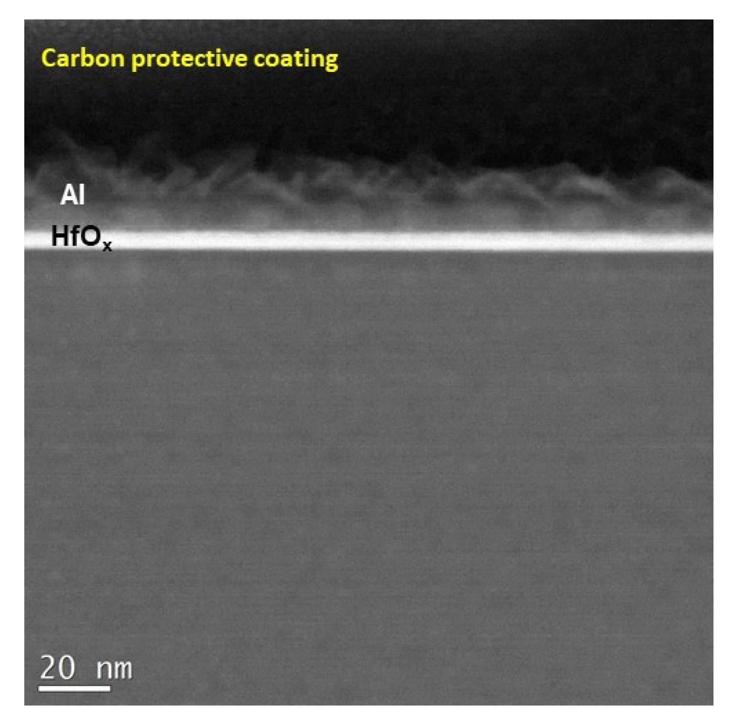
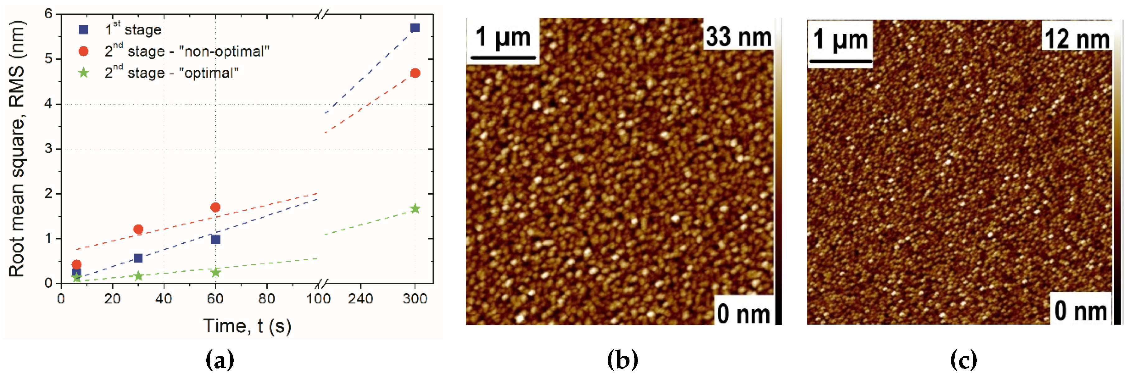
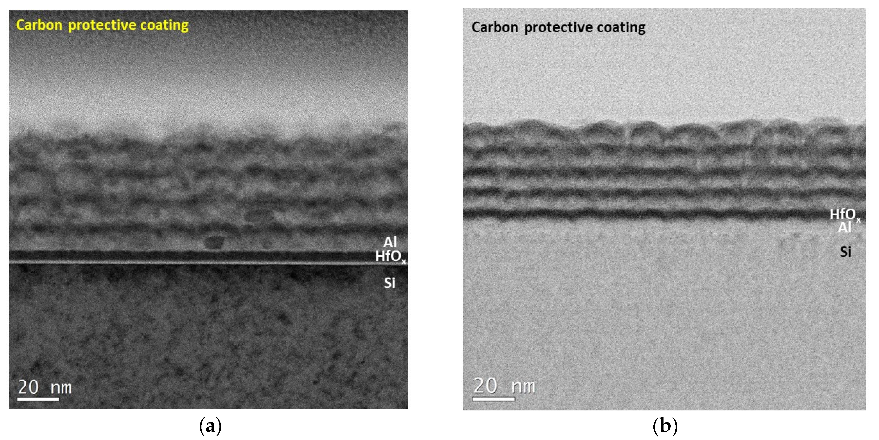
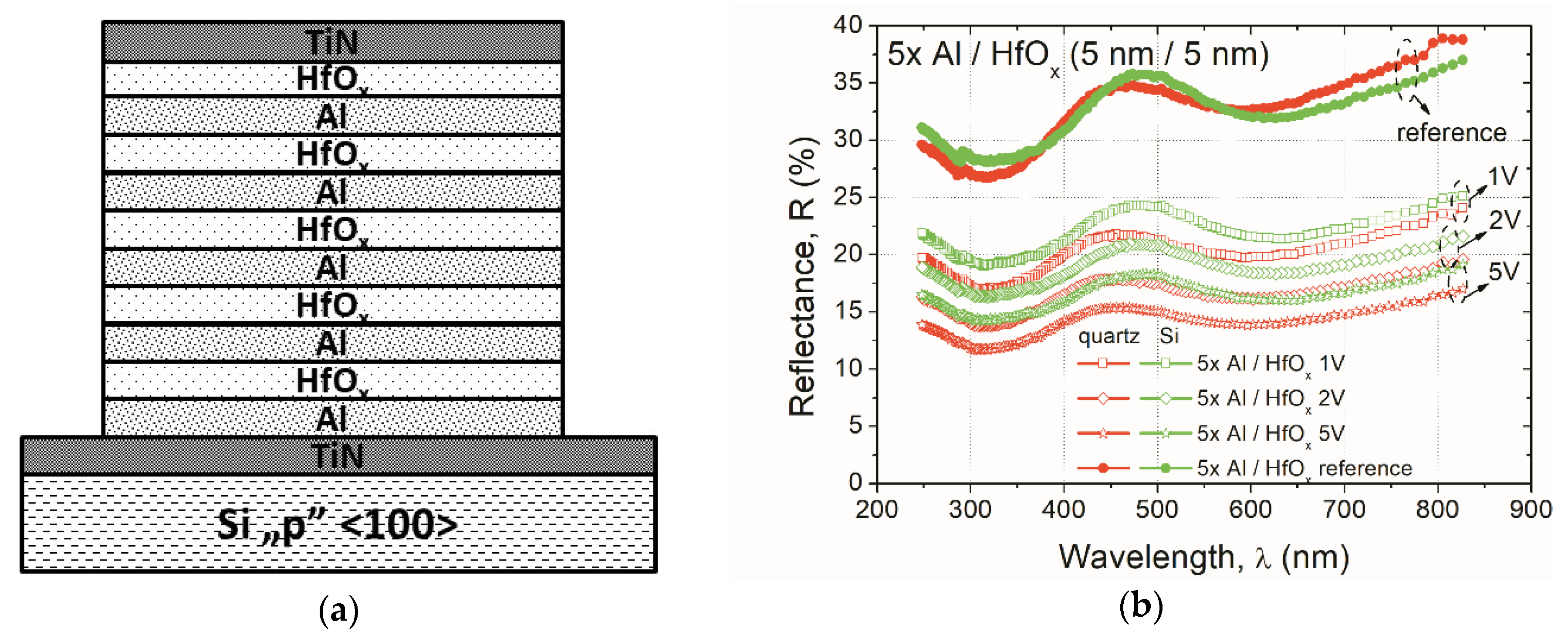
3.2. Fabrication and Characterization of Structures Based on the Multilayers

In this part of the study, the technology of multilayer structure composed of alternating hafnium oxide and aluminum layers was developed. The ultimate application of optimized processes was demonstrated in Figure 6. The fabricated multilayer structures contain 5x Al/HfOx stack. The thickness of each film during the formation was set at ~5 nm.
The micrographs shown in Figure 6 indicates the improved homogeneity of the stack fabricated using the ‘optimal’ recipe of Al sputtering (Figure 6b). It is worth underline that both cross-sections were depicted with the same scale. Moreover, the order of fabricated materials is different to emphasize the influence of the inhomogeneity of the Al film thickness onto the dielectric material that is characterized by a very smooth surface. As can be seen, although the total thickness of fabricated stacks could be estimated around 50 nm, the thickness of the structure formed with ‘non-optimal’ and ‘optimal’ recipe is approximated at ~75 nm, and ~55 nm, respectively. This is due to the much larger roughness level of Al film deposited by the ‘non-optimal’ recipe. It can be also clearly noticed that due to the improvement of homogeneity of Al film, around 30% of the reduction of a total thickness of fabricated stack was demonstrated.
In the last part of this study, the technology of Al/HfOx stack with the titanium nitride (TiN) contacts was developed. The structures were fabricated according to the scheme presented in Figure 7a. Investigated structures were fabricated purposely on both silicon and quartz substrates, to perform comprehensive optical characterization and comparison of obtained results. Titanium nitride electrodes were formed using the pure titanium target (i.e., 99.999% of purity level) in reactive mode with argon, and nitrogen-based plasma. The thickness of TiN films was adjusted to maintain a low resistivity level of the conductive film. After the formation of the multilayer stack, the annealing process was performed at 200 °C in a vacuum atmosphere, in order to improve the insulating properties of the HfOx layer according to our previous studies [38]. Simultaneously, the selected value of the temperature does not affect the stability and the chemical composition of the investigated multilayer stack.
The fabricated structures were characterized optically in the range of 250 nm to 830 nm employing ‘effective’ (i.e., the whole stack based on TiN/ Al/HfOx (5x) /TiN stack) reflectance measurements using spectroscopic ellipsometer set to reflectance measurement mode. The especially developed adapter was used for the characterization of structures with external electrical (DC range) polarization in situ. During the measurements, the bottom TiN electrode was grounded, while the top electrode was polarized by a specific voltage value. The resulting changes of reflectance of investigated devices due to the electrical polarization are depicted in Figure 7b. The typical reference characteristics, i.e., without any external electrical polarization, of structures fabricated on both types of substrate, show almost similar character with the lowest reflectivity value ~27% at 320 nm. Then, the reflectance is increased up to ~38% at 830 nm. The application of electrical polarization results in a visible decrease of reflectance level and it is dependent on voltage value applied to the top TiN electrode. The higher the voltage value the lower the effective reflectance of the investigated stack. For the highest voltage value (i.e., 5 V) in the case of a structure fabricated on a quartz substrate, the decrease of reflectance of the order of 15% and 21%, at 320 nm and 830 nm, respectively, were observed. In the case of a silicon substrate, the corresponding decrease of the order of 14% and 18%, respectively, were noticed. Unfortunately, due to the high absorbance of TiN films, i.e., the effective transmittance level of the investigated stacks was of the order of 5% and it was not possible to investigate the changes of this optical parameter as the effect of electrical polarization. The presented results of the optical response of fabricated test structures due to the electrical polarization are preliminary ones. Further examinations of optical properties of fabricated structures need to be performed, especially at a larger spectral range. However, the findings presented in this work are very promising for applications of multilayer structures in novel photonic devices based on hyperbolic metamaterials in the future.

4. Conclusions

This work was aimed at the development of the technology of ultra-thin aluminum layers with improved thickness homogeneity and reduced roughness level. The optimization procedure was performed using the Taguchi orthogonal tables approach. The Al films were fabricated employing a pulsed-DC magnetron sputtering process. The presented findings allowed for the deposition of conductive films with a smaller dimension of Al domains and lower roughness level as compared to the non-optimized fabrication procedure. Then, the selected set of process parameters was used in the fabrication of stacks based on alternative ultra-thin aluminum and hafnium oxide layers (Al/HfOx). Performed optical characterization in the range of 250 nm to 830 nm demonstrated the possibility to tune the ‘effective’ reflectivity of investigated multilayer stacks due to the external electrical polarization in situ. The increase of the polarization voltage value allowed for a controlled decrease of the reflectance in the range of ~14% and ~20%, at 1V and 5V, respectively. The presented results are promising for the application of multilayer structures in novel photonic devices based on hyperbolic metamaterials; however, further optical investigations at larger spectral ranges are needed.

Author Contributions

Conceptualization and idea of this study, R.M.; Taguchi methodology, D.I., and R.M.; optical measurements, D.I., B.F., and R.M.; structural measurements and analysis of results, M.O., M.Ś., A.G., M.Z. and M.G.; writing—original draft preparation, R.M.; writing—review and editing, R.M.; visualization, D.I., B.F., M.O., M.Ś., A.G., and R.M.; supervision, R.M.; project administration, R.M.; funding acquisition, R.M. All authors have read and agreed to the published version of the manuscript.

Funding

This work has been supported by The National Centre for Research and Development (NCBiR) under grant No. TECHMATSTRATEG1/347012/3/NCBR/2017 (HYPERMAT) in the course of “Novel technologies of advanced materials—TECHMATSTRATEG”.

Acknowledgments

The authors acknowledge the Mariusz Andrzejczuk from the Faculty of Materials Science and Engineering of Warsaw University of Technology, for the TEM measurements and analysis of results.

Conflicts of Interest

The authors declare no conflict of interest.

References

  1. Wilson, R.J.; Weiss, B.L. A review of the properties of aluminium alloy films used during silicon device fabrication. Vacuum 1991, 42, 719–729. [Google Scholar] [CrossRef]
  2. Sequeda, F.O. Thin film deposition techniques in microelectronics. JOM 1986, 38, 55–65. [Google Scholar] [CrossRef]
  3. Kamoshida, K.; Makino, T.; Nakamura, H. Preparation of low-reflectivity Al–Si film using dc magnetron sputtering and its application to multilevel metallization. J. Vac. Sci. Technol. B 1985, 3, 1340. [Google Scholar] [CrossRef]
  4. Krawczak, E.; Gułkowski, S. Electrical Properties of Aluminum Contacts Deposited by DC Sputtering Method for Photovoltaic Applications. Available online: https://www.e3s-conferences.org/articles/e3sconf/abs/2017/07/e3sconf_eems2017_03011/e3sconf_eems2017_03011.html (accessed on 8 May 2020).
  5. Liua, Y.; Zhang, X. Metamaterials: A new frontier of science and technology. Chem. Soc. Rev. 2011, 40, 2494–2507. [Google Scholar] [CrossRef]
  6. Huo, P.; Zhang, S.; Liang, Y.; Lu, Y.; Xu, T. Hyperbolic Metamaterials: Hyperbolic Metamaterials and Metasurfaces: Fundamentals and Applications (Advanced Optical Materials 14/2019). AOM 2019, 7, 1801616. [Google Scholar] [CrossRef] [Green Version]
  7. Veselago, V.G. The electrodynamics of substances with simultaneously negative values of ε and μ. Soviet Physics Uspekhi 1968, 10, 509–517. [Google Scholar] [CrossRef]
  8. Ferrari, L.; Wu, C.; Lepage, D.; Zhang, X.; Liu, Z. Hyperbolic metamaterials and their applications. Prog. Quan. Electr. 2015, 40, 1–40. [Google Scholar] [CrossRef]
  9. Poddubny, A.N.; Iorsh, I.; Belov, P.; Kivshar, Y. Hyperbolic metamaterials. Nat. Photon. 2013, 7, 948–957. [Google Scholar] [CrossRef]
  10. Ishii, S.; Kildishev, A.V.; Narimanov, E.; Shalaev, V.M.; Drachev, V.P. Sub-wavelength interference pattern from volume plasmon polaritons in a hyperbolic medium. Laser Photon. Rev. 2013, 7, 265–271. [Google Scholar] [CrossRef]
  11. Jacob, Z.; Smolyaninov, I.; Narimanov, E. Broadband Purcell effect: Radiative decay engineering with metamaterials. Appl. Phys. Lett. 2012, 100, 181105. [Google Scholar] [CrossRef] [Green Version]
  12. Poddubny, A.N.; Belov, P.A.; Kivshar, Y.S. Spontaneous radiation of a finite-size dipole emitter in hyperbolic media. Phys. Rev. A 2011, 84, 023807. [Google Scholar] [CrossRef] [Green Version]
  13. Gu, L.; Tumkur, T.U.; Zhu, G.; Noginov, M.A. Blue shift of spontaneous emission in hyperbolic metamaterial. Sci. Rep. 2014, 4, 4969. [Google Scholar] [CrossRef] [PubMed] [Green Version]
  14. Taya, S.A.; Qadoura, I.M. Slab waveguide with air core layer and anisotropic left-handed material claddings as a sensor. Optik–Int. J. Light Electron. Opt. 2013, 124, 1431–1436. [Google Scholar] [CrossRef]
  15. Neira, A.D.; Wurtz, G.A.; Zayats, A.V. Superluminal and stopped light due to mode coupling in confined hyperbolic metamaterial waveguides. Sci. Rep. 2015, 8, 17678. [Google Scholar] [CrossRef] [Green Version]
  16. Rizza, C.; Ciattoni, A.; Spinozzi, E.; Columbo, L. Terahertz active spatial filtering through optically tunable hyperbolic metamaterials. Opt. Lett. 2012, 37, 3345–3347. [Google Scholar] [CrossRef] [Green Version]
  17. Othman, M.A.K.; Guclu, C.; Capolino, F. Graphene-based tunable hyperbolic metamaterials and enhanced near-field absorption. Opt. Expr. 2013, 21, 7614–7632. [Google Scholar] [CrossRef] [Green Version]
  18. Yin, G.Z.; Jillie, D.W. Orthogonal design for process optimization and its application in plasma etching. Solid State Technol. 1987, 30, 127–132. [Google Scholar]
  19. Lye, L.M. Tools and toys for teaching design of experiments methodology. In Proceedings of the 33rd Annual General Conference of the Canadian Society for Civil Engineering, Toronto, ON, Canada, 2–4 June 2005. [Google Scholar]
  20. Montgomery, D.C. Design and Analysis of Experiment; Wiley: New York, NY, USA, 2005. [Google Scholar]
  21. Ilzarbe, L. Practical applications of design of experiments in the field of engineering: A bibliographical review. Qual. Reliab. Eng. Int. 2008, 24, 417–428. [Google Scholar] [CrossRef]
  22. Dean, A.; Voss, D.; Draguljić, D. Design and Analysis of Experiments, 2nd ed.; Springer: Berlin, Germany, 2017. [Google Scholar] [CrossRef]
  23. Storn, R.; Price, K.J. Differential Evolution—A Simple and Efficient Heuristic for global Optimization over Continuous Spaces. Glob. Optimiz. 1997, 11, 341–359. [Google Scholar] [CrossRef]
  24. Daneshvar, N.; Khataee, A.R.; Rasoulifard, M.H.; Pourhassan, M. Biodegradation of dye solution containing Malachite Green: Optimization of effective parameters using Taguchi method. J. Hazard. Mat. 2007, 143, 214–219. [Google Scholar] [CrossRef]
  25. Tasirin, S.M.; Kamarudin, S.K.; Ghani, J.A.; Lee, K.F. Optimization of drying parameters of bird’s eye chilli in a fluidized bed dryer. J. Food Eng. 2007, 80, 695–700. [Google Scholar] [CrossRef]
  26. Wu, C.-H.; Chen, W.-S. Injection molding and injection compression molding of three-beam grating of DVD pickup lens. Sens. Actuat. A Phys. 2006, 125, 367–375. [Google Scholar] [CrossRef]
  27. Houng, J.-Y.; Liao, J.-H.; Wu, J.-Y.; Shen, S.-C.; Hsu, H.-F. Enhancement of asymmetric bioreduction of ethyl 4-chloro acetoacetate by the design of composition of culture medium and reaction conditions. Process. Biochem. 2007, 42, 1–7. [Google Scholar] [CrossRef]
  28. Romero-Villafranca, R.; Zúnica, L.; Romero-Zúnica, R. Ds-optimal experimental plans for robust parameter design. J. Statist. Plan. Inferen. 2007, 137, 1488–1495. [Google Scholar] [CrossRef]
  29. Elshennawy, A.K. Quality in the new age and the body of knowledge for quality engineers. Total Qual. Manag. Bus. Excell. 2004, 15, 603–614. [Google Scholar] [CrossRef]
  30. Ibrahim, I.H.; Ng, E.Y.K.; Wong, K.W.L. Applying Taguchi’s off-line quality control method and ANOVA on the maneuverability of the F-5E intake. Math. Comp. Model. 2009, 49, 1359–1371. [Google Scholar] [CrossRef]
  31. Mroczyński, R.; Beck, R.B. Silicon oxynitride layers fabricated by Plasma Enhanced Chemical Vapor Deposition (PECVD) for CMOS devices. ECS Trans. 2009, 25, 797–804. [Google Scholar] [CrossRef]
  32. Kieliszczyk, M.; Janaszek, B.; Tyszka-Zawadzka, A.; Szczepański, P. Guided Optical Modes in Metal-Cladded Tunable Hyperbolic Metamaterial Slab Waveguides. Crystals 2020, 10, 176. [Google Scholar] [CrossRef] [Green Version]
  33. Kieliszczyk, M.; Janaszek, B.; Tyszka-Zawadzka, A.; Szczepański, P. Tunable spectral and spatial filters for the mid-infrared based on hyperbolic metamaterials. Appl. Opt. 2018, 57, 1182. [Google Scholar] [CrossRef]
  34. Kieliszczyk, M.; Janaszek, B.; Tyszka-Zawadzka, A.; Szczepański, P. Multiresonance response in hyperbolic metamaterials. Appl. Opt. 2018, 57, 2135–2214. [Google Scholar] [CrossRef]
  35. Ottone, C.; Laurenti, M.; Bejtka, K.; Sanginario, A.; Cauda, V. The effects of the film thickness and roughness in the anodization process of very thin aluminum films. J. Mater. Sci. Nanotechnol. 2014, 1, S107. [Google Scholar] [CrossRef] [Green Version]
  36. Lita, A.E.; Sanchez, J.E., Jr. Characterization of surface structure in sputtered Al films: Correlation to microstructure evolution. J. Appl. Phys. 1999, 85, 876–882. [Google Scholar] [CrossRef] [Green Version]
  37. Paul, A.; Wingbermuhle, J. Surface morphology for ion-beam sputtered Al layer with varying sputtering conditions. Appl. Surf. Sci. 2006, 252, 8151–8155. [Google Scholar] [CrossRef]
  38. Szymańska, M.; Gierałtowska, S.; Wachnicki, Ł.; Grobelny, M.; Makowska, K.; Mroczyński, R. Effect of reactive magnetron sputtering parameters on structural and electrical properties of hafnium oxide thin films. Appl. Surf. Sci. 2014, 301, 28–33. [Google Scholar] [CrossRef]
Figure 1. Surface topography of 30 nm Al films sputtered using pulsed-DC magnetron sputtering process: (a) HR-SEM, and (b) AFM micrographs.
Crystals 10 00384 g001
Figure 2. The cross-section (HR-TEM, Z-contrast) of Al/HfOx stack fabricated on a silicon substrate using a pulsed-DC magnetron sputtering process.
Crystals 10 00384 g002
Figure 3. Influence of magnetron sputtering process’ parameters onto roughness of aluminum films: (a) pressure in the reactive chamber, (b) DC power applied to the electrodes, (c) argon flow, and (d) time of the process.
Crystals 10 00384 g003
Figure 4. (a) Comparison of the roughness level of aluminum films fabricated using investigated sputtering procedures, and AFM micrographs of Al surface after formation using (b) ‘non-optimal’ (RMS = 4.8 nm), and (c) ‘optimal’ (RMS = 1.7 nm) recipe; sputtering time = 300 s.
Crystals 10 00384 g004
Figure 5. Comparison of the surface state of aluminum films fabricated using: (a,b) ‘non-optimal’, and (c,d) ‘optimal’ recipe; the thickness, and RMS factor of examined films was also depicted.
Crystals 10 00384 g005
Figure 6. Comparison of HR-TEM cross-sections of structure based on alternative (5x) Al and HfOx layers fabricated by pulsed-DC magnetron sputtering processes; Al film was sputtered through the (a) ‘non-optimal’, and (b) ‘optimal’ recipe; the thickness of each film was set at ~5 nm.
Crystals 10 00384 g006
Figure 7. (a) Schematic cross-section of structure based on alternative (5x) Al and HfOx layers investigated in this study, and (b) change of effective reflectance of examined stacks due to the external electrical polarization; the thickness of Al, HfOx, and TiN films was set at ~5 nm, ~5 nm, and 50 nm, respectively.
Crystals 10 00384 g007
Table 1. Selected values of pulsed-DC reactive magnetron sputtering process’ selected for the optimization of aluminum films using L9(43) orthogonal table.
Pressure
(mTorr)
DC Power
(W)
Ar Flow
(sccm)
Time
(s)
5751560
1010020120
1512525300
Table 2. Selected values of pulsed-DC reactive magnetron sputtering process’ selected for the optimization of aluminum films using L25(45) orthogonal table.
Pressure
(mTorr)
DC Power
(W)
Ar Flow
(sccm)
Time
(s)
3501010
5751560
101002090
1515025120
2020030180

