

Abstract
In this paper, a novel double-step (DS) structure tunnel field-effect transistor with a linear doping profile channel (DSS-LDC-TFET) is presented. The use of a step-shaped structure near the source/channel interface leads to the large tunneling junction area because the band-to-band tunneling of the carriers occurs perpendicularly along the conducting path in the channel. The step-shape of the channel/drain interface reduces the electric field distribution near the drain junction which helps to suppress the ambipolar behavior. Further, the DS structure of the body suppresses the ambipolar conduction due to increasing the effective length of channel area along the device. Therefore, the height of the steps in the proposed structure plays an important role in the device characteristics. The doping profile in the channel region is considered to be linear. The maximum value of the doping concentration is at the source side and linearly decreases to its minimum value along the x-axis. Numerical simulation results show that using the linear doping distribution at the channel improves device behavior through reducing the tunneling barrier width at the source/channel interface. The optimum length for the linear-doped part of the channel is selected to maximize the on-state current without degrading much the off-state current. Finally, the comparative study between DSS-LDC-TFET with the conventional silicon-on-insulator tunnel field-effect transistor is presented.
Export citation and abstract BibTeX RIS
1. Introduction
Nowadays, the continuous down-scaling of channel length (feature size) in CMOS technology has led to several problems. The most important cases of these problems are short channel effects, high off-state leakage current and poor subthreshold slope (SS) [1–10]. The smallest value of subthreshold slope that can be achieved in a MOSFET is 60 mV dec−1 because the transport of charge carriers over the potential barrier is a thermionic process [10]. The tunnel field-effect transistor (TFET) has been suggested as an excellent alternative for conventional MOSFET due to the different mechanism of carriers injection from source to channel [11, 12]. The TFET is actually a gate-controlled reverse biased P-I-N diode that employs band-to-band tunneling (BTBT) as a new current transport mechanism [13–16]. Thus, the leakage current of a TFET is very low and also it is able to theoretically achieve a smaller SS [16–18]. Besides all of these merits, the Si-based conventional TFETs have two major drawbacks [19–22]: low on-state current (Ion) due to the limited BTBT probability and ambipolar conduction (Iamb) which is caused by BTBT at drain junction. In order to overcome these drawbacks, various techniques have been reported in earlier research works i.e. bandgap engineering [23–25], double-gate architecture [26, 27], gate work function engineering [28–32], hetero-dielectric TFET [33, 34], strain channel engineering [35, 36], different geometries such as L-shaped and U-shaped channel TFET [37–45] and so on. In this paper, we have proposed a novel TFET design with a linear-doped channel double-step structure for the first time. The results of technology computer-aided design (TCAD) simulations demonstrate the advantages of using the presented device structure. The electrical characteristics of the proposed TFET are investigated while varying both the linear doping profile in the channel and the height of steps. Then, the results are compared with the characteristics of a conventional silicon-on-insulator tunnel field-effect transistor (SOI-TFET). The rest of the paper is organized as follows. Section 2 describes the structure of the proposed device and the applied physical models. Effects of structural parameters on the electrical characteristics of proposed TFET are presented in section 3. Section 4 focuses on the electrical performance of double-step structure tunnel field-effect transistor with a linear doping profile channel (DSS-LDC-TFET) in comparison with conventional SOI-TFET. Finally, section 5 presents the conclusions.
2. Device structure and simulation setup
Figures 1(a) and (b) show a conventional SOI-TFET and the proposed TFET with double-step structure, respectively. The channel length (LCH) is 20 nm, the length of the source and drain regions is 10 nm, the silicon body (tbody) and the buried-oxide thicknesses are 10 nm and 20 nm, respectively. HfO2 is used with 2 nm thickness as the gate dielectric layer. The work function of the gate material is 4.17 eV [42]. For the double-step structure, Lstep is fixed at 5 nm. Figure 1(c) shows the energy band diagrams for the conventional SOI-TFET to illustrate how the band-to-band tunneling is achieved. As can be seen in the figure, in order to occure the carriers tunneling at the source/channel junction, two conditions are required. First, the valence band of the source (EV) should be aligned with the conduction band (EC) of the channel. Second, the width of the potential barrier (Wt) should be small enough to allow the carriers tunneling. All the simulations to study the electrical characteristics of the proposed structure are carried out using Silvaco-Atlas device simulator [46].

Figure 1. Schematic of simulated device architectures (a) conventional SOI-TFET and (b) DSS-LDC-TFET. (c) The energy band diagrams of the conventional SOI-TFET illustrate how the band-to-band tunneling is achieved.
Download figure:
Standard image High-resolution imageThe nonlocal BTBT model takes into account the rate of carriers tunneling over the effective tunneling volume. As shown in figure 2, this model is calibrated with the models used in [42] which is already calibrated to tunneling models of [8]. The other physical models such as Lombardi mobility model, bandgap narrowing model, Fermi–Dirac statistics, Auger and Shockley-Read-Hall recombination models are also included.

Figure 2. Reproduction of the reported result from [42].
Download figure:
Standard image High-resolution image3. Effects of structural parameters (t1, t2 and LLD) on the electrical characteristics of DSS-LDC-TFET
As shown in detail in figure 1, there are two main differences between the proposed and conventional TFET structures: geometric difference and the doping profile of the channel region. Note that by appropriate selection of design variables, the optimized structure is achieved. In this section, numerical simulations are performed to study the influence of various key parameters such as the length of laterally linear doping distribution in the channel region (LLD), the height of step structure at channel/drain junction (t2) and the height of step structure near the source/channel junction (t1) on the electrical characteristics of the proposed novel device architecture. Moreover, the optimum values of these key parameters to optimize the performance of a DSS-LDC-TFET can be achieved based on the simulation results.
3.1. Effects of channel doping with a linear profile (LLD)
The different lateral doping profiles along the device are shown in figure 3. The source and drain regions are uniformly doped p-type (1020 cm−3) and n-type (5 × 1018 cm−3), respectively. The doping profile of the channel region is laterally non-uniform (n-type) with peak doping concentration (1020 cm−3) at the source side. The concentration of carriers decreases from the peak value down to the minimum doping level (1016 cm−3) with a linear drop-off function along the channel. The various shapes of the doping profile can be obtained by changing the slope of this linear function.

Figure 3. The linear variation of channel doping profile with different slopes along lateral position.
Download figure:
Standard image High-resolution imageAs shown in figure 1(b), the doping profile inside the source and drain regions is uniform whereas, the channel region is segmented into two regions with linear and uniform doping distribution. LLD and LUD are related to the length of these regions. The energy-band diagrams to explore the effects of the linear-doped channel on the performance of TFET are shown in figure 4. It is observed that the continuous linear reduction of the doping profile at the tunneling junction (near the source side) reduces the tunneling barrier width and so increases the tunneling carriers.

Figure 4. The energy-bands profile of the linear-doped SOI-TFET along the lateral position.
Download figure:
Standard image High-resolution imageThe transfer characteristics of the LDC-TFET for the different channel doping profile are shown in figure 5. As indicated before, the larger LLD can cause higher on current due to the narrower tunneling barrier. In the other hand, reducing the doping of the channel slowly, causes that more carriers in the source/channel interface have a chance to cross the tunneling barrier. It should be noted that with increasing the length of the linear-doped part in the channel region, the gate voltage where the BTBT first occurs shifts to lower values, and so the off-state current significantly is degraded. The off-state current (the drain to source current when the gate to source voltage is equal to zero) determines the amount of power that is dissipated when the device operating mode is off. Thus, it is clear that the lowest possible value is desirable for this current to have the minimum dissipation of power. Therefore, the best choice for channel doping profile is when the threshold voltage of carriers tunneling is set to 0 V. In the other words, the optimum value of LLD can be found based on maximizing the on-state current without degrading much the off-state current.

Figure 5. Drain current versus gate voltage for different channel doping profiles.
Download figure:
Standard image High-resolution image3.2. Effects of step height at the drain side (t2)
The objective of this section is to investigate the impact of step height at drain side (t2) on the performance of TFET. In order to do so, the off-state energy-band diagrams of DSS-TFET for the variation of t2 at fixed t1 = 0 nm are depicted in figure 6. It is clearly observed that by increasing the height of the step, the length of the tunneling path is effectively increased. The tunneling probability exponentially depends on the length of tunneling path [47]. Thus, the probability of carriers tunneling through the potential barrier decreases.

Figure 6. Influence of t2 (the height of the step at the drain side) on the energy-band diagrams in the off-state conditions.
Download figure:
Standard image High-resolution imageOn the other hand, the proposed TFET with a step-shaped structure at channel/drain interface reduces the electric field intensity (which is created by the gate voltage) on the drain side by increasing the distance between the gate and drain electrodes. This is shown in figure 7.

Figure 7. Simulated diagrams of the electric field at VGS = −1V and VDS = 0.7V (a) conventional structure, (b) step structure near drain side.
Download figure:
Standard image High-resolution imageFigure 8 shows simulated transfer characteristics for the proposed structure of TFET with the height of step at channel/drain interface (t2) as a parameter. According to the aforementioned analysis and since the rate of BTBT generation is highly dependent on the electric field [42], the increase in t2 decreases the ambipolar current. This reduction can be attributed to the lower BTBT at the channel/drain junction.

Figure 8. Drain current vs. gate-to-source voltage characteristics for different values of t2.
Download figure:
Standard image High-resolution image3.2.1. IAMB variation against t2.
As shown in figure 9, the data points that were extracted from the simulation results (figure 8) can be well estimated with an exponential function (linear function in the logarithmic scale) in the following form


Figure 9. The dependence of the ambipolar current to the step height at drain side, extracted from the simulation (discrete points). Dashed line represents the exponential fit.
Download figure:
Standard image High-resolution imageThis model can be useful for predicting the ambipolar behavior of the device when t2 changes.
3.2.2. IDS variation against VGS in ambipolar-state.
As t2 increases, the slope of the ambipolar current reduction decreases. It is according to the exponential dependence of this current to the step height at drain side. As shown in figure 10, the symbols that are related to the ambipolar region of I–V curve (the gate to source voltage more negative than the starting voltage of carriers tunneling at channel/drain junction) were obtained from the TCAD simulation results and can be well fitted with an exponential function in the following form

where a and b are the fitting parameters. The values of these parameters are shown in table 1 for the different values of t2.

Figure 10. The I–V curves for different values of t2, obtained from the TCAD simulations (symbols). Solid lines represent the exponential fit.
Download figure:
Standard image High-resolution imageTable 1. The values of fitting parameters for the different values of t2.
| t2 (nm) | a (× 10−27) | b |
|---|---|---|
| 1 | 474.7 | −27.19 |
| 2 | 6.248 | −29.06 |
| 3 | 2.901 | −27.24 |
| 4 | 8.814 | −23.64 |
| 5 | 3094 | −15.64 |
| 6 | 4862 × 103 | −6.914 |
| 7 | 3192 × 105 | −2.277 |
3.3. Effects of step height at the source side (t1)
The on-state energy-band diagrams of DSS-TFET for the variation of t1 at fixed t2 = 0 nm are shown in figure 11. As previously seen the step-shaped structure at drain side leads to an obvious reduction in tunneling barrier width while based on figure 11 the height of step at source side (t1) does not have much effect on the tunneling barrier width and only increases the tunneling volume. The width of potential barrier (Wt) is fixed at Lstep which is smaller than for the conventional structure. So the average subthreshold-slope (SSavg) is reduced due to increased tunneling probability for smaller Wt. The lower value of SSavg is equal to more abrupt OFF to ON transition. On the other hand, it can be said that by increasing t1, the lower gate to source voltage is required to achieve 10–7 A μm−1 of IDS (the threshold voltage has been chosen at the point where IDS is equal to 10–7 A µm−1).

Figure 11. Influence of t1 (the height of the step at the source side) on the energy-band diagrams in the on-state conditions.
Download figure:
Standard image High-resolution imageFigure 12 shows the transfer characteristics for the proposed device structure. The step height at the drain side (t2) is fixed at 0 nm while the step height at the source side is varied. As shown in the figure, the on-state current becomes higher as t1 increases. The increase of Ion is due to the larger BTBT area at the source/channel junction. The tunneling junction is perpendicular to the channel direction and this is the reason for the formation of a larger tunneling area.

Figure 12. Drain current vs. gate-to-source voltage characteristics for different values of t1.
Download figure:
Standard image High-resolution imageThis tunneling junction area and the electric field at VGS = 1 V and VDS = 0.7 V are shown in figure 13. Therefore, in order to achieve a higher on-state current, the BTBT generation rate can be enhanced by increasing t1.

Figure 13. Simulated diagrams of the electric field at VGS = 1V and VDS = 0.7V (a) conventional structure, (b) step structure near source side.
Download figure:
Standard image High-resolution image3.3.1. ION variation against t1.
In the proposed structure of TFET as t1 increases, the vertical BTBT area increases in proportion, so the on-state current changes linearly against the t1. As shown in figure 14, the discrete points that were extracted from the I–V characteristics (figure 12) can be well fitted with a linear function in the following form


Figure 14. The dependence of the on-state current to the step height at source side, extracted from the simulation (discrete points). Dashed line represents the linear fit.
Download figure:
Standard image High-resolution imageThis model can be useful for predicting the on-state behavior of the device when t1 changes.
3.3.2. IDS variation against VGS (above threshold).
As t1 increases, the slope of the on-state current increment is constant. It is according to the linear dependence of this current to the step height at source side. As shown in figure 15, the symbols are related to the I–V curve of the device that were obtained from the TCAD simulation results. These symbols in the above threshold region can be well fitted with a power function in the following form

where a and b are the fitting parameters. The values of these parameters are shown in table 2 for the different values of t1.

Figure 15. The I–V curves for different values of t1, obtained from the TCAD simulations (symbols). Solid lines represent the power fit.
Download figure:
Standard image High-resolution imageTable 2. The values of fitting parameters for the different values of t1.
| t1 (nm) | a (× 10−6) | b |
|---|---|---|
| 10 | 1.5 | 5.462 |
| 9 | 1.33 | 5.4956 |
| 8 | 1.17 | 5.5308 |
| 7 | 1 | 5.5866 |
| 6 | 0.8 | 5.6752 |
| 5 | 0.6 | 5.8045 |
4. Electrical performance analysis
In the previous sections, the proposed structure of TFET, named as DSS-LDC-TFET was introduced and the impact of three structural parameters (t1, t2 and LLD) on its electrical characteristics was investigated in detail. Now, the focus of this section is on digital and analog performance of this structure in comparison with conventional SOI-TFET.
4.1. DC-performance metrics
Figure 16 shows the transfer characteristics of the presented DSS-LDC-TFET and the conventional SOI-TFET structure. From the curve, it is observed that the proposed device shows better electrical characteristics in terms of significant on-state current, less ambipolar-state current and the higher Ion/Ioff current ratio. It should be noted that the final structure of the proposed device is also shown in figure 16, and based on the simulation results, the optimum values of the variable parameters are suggested.

Figure 16. Simulated transfer characteristics of a planar SOI-TFET and the final optimized DSS-LDC-TFET.
Download figure:
Standard image High-resolution imageTable 3 shows the device performance parameters such as on-state current (Ion), off-state current (Ioff), Ion/Ioff, ambipolar-state current (Iamb), average subthreshold-slope (SSavg), threshold voltage (VTH) and drain induced barrier lowering (DIBL) for the proposed DSS-LDC-TFET and the conventional SOI-TFET. The on-state, off-state and ambipolar-state have been chosen at the point where VGS is equal to 1 V, 0 V and −1 V, respectively [31]. Obviously, significant improvements are observed in the majority of device performance metrics.
Table 3. Different device performance metrics for the two different structures of TFET.
| Structures | Ion (A µm−1) | Ioff (A µm−1) | Ion/Ioff | Iamb (A µm−1) | SSavg (mV dec−1) | VTH (V) | DIBL (mV V−1) |
|---|---|---|---|---|---|---|---|
| Conventional SOI-TFET | 5.18 × 10⁻⁷ | 1.99 × 10⁻¹⁸ | 2.6 × 10¹¹ | 6.06 × 10⁻¹² | 72.9 | 0.78 | 466 |
| DSS-LDC-TFET | 2.62 × 10⁻⁶ | 4.3 × 10⁻¹⁸ | 0.6 × 10¹² | 4.44 × 10⁻¹⁸ | 51.2 | 0.53 | 33.3 |
4.2. Analog performance
In the rest of this section, the transconductance and cut-off frequency have been studied to evaluate the performance of the presented architecture in analog applications. The transconductance (gm) of the DSS-LDC and conventional TFET structures in terms of the applied gate to source voltage are shown in figure 17. It is observed that the gm of a DSS-LDC-TFET is significantly higher than the conventional SOI-TFET. This is because of the increased transmission of charge carriers from the source to the channel region.
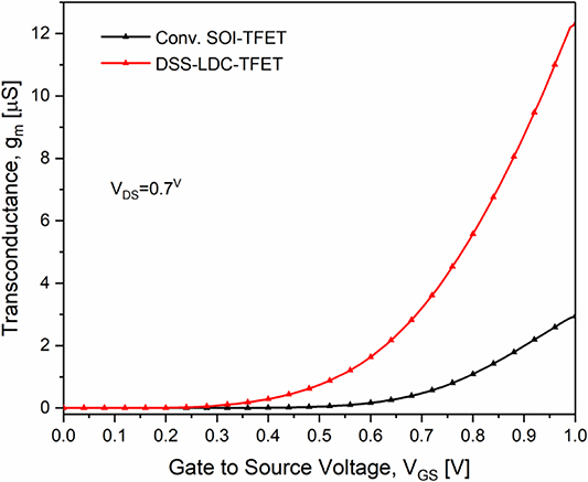
Figure 17. The transconductance curves as a function of VGS for the two different structures of TFET.
Download figure:
Standard image High-resolution imageFigure 18 shows the variation of cut-off frequency (fT) versus the gate to source voltage for the two different architectures of TFET. It is clear from the figure that the cut-off frequency of DSS-LDC-TFET is higher compared to conventional SOI-TFET. This enhancement is due to an increment in transconductance as earlier reported in figure 17, and also due to the reduction of the gate to drain capacitance. The proposed architecture has a smaller capacitor between gate and drain due to the larger distance between these electrodes. Thus, increasing the cut-off frequency of the presented structure makes it possible to design faster circuit elements.

Figure 18. The cut-off frequency versus VGS for the two different structures of TFET.
Download figure:
Standard image High-resolution image
5. Conclusion
In this paper, a linear-doped channel novel TFET with a double-step structure is proposed and investigated. The numerical simulation results clearly demonstrate that the proposed DSS-LDC-TFET has more advantages compared with the conventional SOI-TFET, in terms of its higher on-state current and lower ambipolar conduction. Improvement of on-current is found when the height of the step structure placed near the source side (t1) is changed to the higher value. This is due to the fact that a larger tunneling junction area has been formed. Increasing the height of the step-shaped structure at the channel/drain interface (t2) reduces the electric field intensity at this junction, which in turn reduces the ambipolar current. Moreover, significant improvements in on-state current can also be achieved using laterally non-uniform doping distribution in the channel region. The length of that part of the channel that has a linear doping profile has been optimized to attain better results in terms of the Ion/Ioff ratio. Finally, a comparative study of device performance parameters of the DSS-LDC-TFET over the conventional SOI-TFET was investigated through the 2D numerical simulations.