


1 Introduction
Diode-pumped solid-state (DPSS) lasers have made great progress in the past decades. One of the enduring obstacles that DPSS lasers have faced is the restriction from high thermal gradients and aberration under intense pumping conditions. However, with the face cooling configuration of a thin, disk-shaped active medium, the diode-pumped architecture allows building high output power solid-state lasers with excellent spatial beam quality and high conversion efficiency. Following the thin disk laser concept introduced by Giesen et al. [Reference Giesen, Hügel, Voss, Wittig, Brauch and Opower1], thin disk lasers have attracted attention because of their various applications in the material processing industry[Reference Huegel and Bohn2, Reference Giesen and Speiser3]. Research conducted on high-power thin disk lasers has primarily focused on Yb:YAG, because Yb-doped materials exhibit considerably lower thermal loading factors (9% if pumping at 940 nm) than Nd-doped counterparts. However, Yb-doped materials require a high pump density to reach the threshold, and are intrinsically sensitive to temperature due to their quasi-three-level nature.
The spectroscopic parameters of the Nd-doped materials are superior to those of the Yb-doped materials. On the one hand, the effective emission cross-section is higher and the system is less sensitive to temperature fluctuations, which offer important practical advantages. On the other hand, the re-absorption effect is negligible. These advantages, combined with lower but reasonable upper-state lifetimes, mean that lower threshold systems might result from the use of Nd-doped materials. A thin disk Nd:GdVO4 laser was reported by Pavel and Taira[Reference Pavel and Taira4]. The continuous-wave (CW) output powers of 13.9 W at 1064 nm for an absorbed power at 808 nm of 22 W and 3.6 W for an absorbed power at 879 nm of 6.2 W were demonstrated. Among the Nd-doped materials, Nd:YVO4 offers several advantages: a large stimulated emission cross-section at 1064 nm, linearly polarized emissions, broad absorption bandwidth and high absorption cross-section at 808 nm pump wavelength, which is particularly advantageous for reducing passes of the pump radiation to achieve efficient absorption. Generally, the  $a$-cut type is used, resulting in a strongly polarized laser emission.
The use of Nd:YVO4 material in thin disk geometry has attracted attention[Reference Kemp, Valentine and Burns5]. Koch et al. employed a thin disk Nd:YVO4 laser with a 10 W pump power, generating a CW output power of 4.4 W at 1064 nm. For the 40 W pump power, a maximum output power of 13.7 W was achieved[Reference Koch, Hollemann, Clemens, Voelckel, Giesen and Voss6]. The possibility of adapting this material to a pulsed-mode operation has been demonstrated[Reference Hollemann, Zimer and Hirt7]. The highest  $Q$-switched pulse energy of 0.27 mJ at 10 Hz has been achieved with a pumping power of 30 W. In addition to the traditional 1064 nm four-level transition, the laser quasi-three-level transition
  $^{4}\text{F}_{3/2}$–
 $^{4}\text{I}_{9/2}$ of a Nd:YVO4 thin disk laser with a 5.8 W output power at 914 nm has been demonstrated[Reference Gao, Larionov, Speiser, Giesen, Douillet, Keupp, Rasel and Ertmer8]. The thin disk geometry is helpful to achieve a compact, efficient and reliable visible light source employing intracavity frequency doubling CW near-infrared lasers. For an incident pump power of 8.65 W, second harmonic (SH) power of 1.3 W at 532 nm was obtained with a PPKTP crystal[Reference Wang, Pasiskevicius, Laurell, Liao, Liu and Miller9]. At a pumping power of 30 W, a maximum output power of 8.9 W at 532 nm was obtained with an LBO crystal[Reference Knoke, Hollemann, Nickel and Voelckel10]. A 2 W CW output power at 457 nm based on LBO was generated[Reference Knoke, Pachomis and Hollemann11]. Pacel et al. employing a 0.3 at.% Nd:YVO4 demonstrated 10.9 W output power at 1064 nm and 6.4 W output power at 532 nm for 27.2 W of 808 nm pump power. At the same time, a 3.2 W output power at 914 nm and 1.6 W output power at 457 nm for 27.2 W of 808 nm pump power were obtained[Reference Stoehr, Rehbein, Douillet, Friebe, Keupp, Mehlstäubler, Wolff, Rasel, Ertmer, Gao and Giesen12].
For the above Nd:YVO4 thin disk laser, low absorption of the pump radiation occurs because the effective absorption path length is twice the thickness of the disk when the pump beam is reflected only once at the backside of the laser crystal. Improvement of absorption efficiency is typically achieved by re-circulating the pump beam in a multipass pumping scheme. However, this complicated and expensive multipass pumping architecture is not desirable for many applications. The double-pass pumping scheme as described by Millar et al. [Reference Millar, Kemp and Burns13] implies the use of highly doped or thick crystals to compensate for the lower absorption. In addition to effective pump absorption, the thermal effects of the crystal must also be considered. In practice, the performance of the Nd:YVO4 thin disk laser in terms of maximum output power, beam quality and efficiency is often affected by thermal effects due to its strong absorption and moderate thermal conductivity. The thermal lens is a critical factor for resonator design. Moreover, the thermal stress will ultimately induce crystal fracture and the spherical aberration will induce degradation in beam quality and resonator losses.
The in-band pumping directly into the emitting level is a method to reduce the thermal load in the Nd:YVO4 thin disk[Reference Pavel, Lünstedt, Petermann and Huber14–Reference Pavel, Kränkel, Peters, Petermann and Huber17]. As a method to reduce thermal effects, composite crystals with undoped end cap have been employed in the bulk crystal system[Reference Zhuo, Li, Li and Yang18]. In addition, researchers have proposed ways to further alleviate thermal effects such as the use of an additional sapphire plate to compress the thin disk crystal for stress compensation[Reference Liao, Miller and Armstrong19–Reference Hua and Miller21] or the simultaneous cooling of two disk faces based on the SiC material[Reference Newburgh and Dubinskii22]. The thermal conductivity of the SiC material is close to that of copper, while the thermal expansion coefficient is closer to that of Nd:YVO4. However, the quantum defect is not the only factor in determining the fractional thermal loading due to a more complicated energy level structure of the Nd:YVO4 material. This means it is susceptible to different detrimental effects such as cross-relaxation, energy transfer upconversion (ETU) and excited-state absorption (ESA), which will cause fractional thermal loading exceeding the quantum defect.
In this paper, a simple, compact double-pass pumped Nd:YVO4 thin disk laser was demonstrated. The schemes of in-band pumping, undoped end face bonds and SiC material heat sink were combined to alleviate the thermal effect. The influence of Nd doping concentration and thickness on the CW performance was experimentally investigated by using two crystals of approximately the same absorption efficiency but different doping concentrations of 1 at.% and 0.5 at.%. At the same time, a numerical analysis of the temperature distribution and thermal lens effect in the laser considering the influence of the ETU effect was presented and compared to the experimental results. The effect of the temperature dependence of the thermal conductivity tensor was also taken into account. The numerical simulations were based on the finite-element analysis methods and carried out using the COMSOL software, which matched well with experimental results. Consequently, the theoretical model can be employed as a useful tool for the design of the distributed face cooling scheme[Reference Kausas, Zheng and Taira23].
2 Theoretical analysis for thermal effects
Generally, the performances of Nd:YVO4 thin disk lasers are affected by thermal effects. Thus, it is significant to conduct an accurate theoretical analysis of the temperature distribution and thermal lens effect for optimum design of the double-pass pumped Nd:YVO4 thin disk laser. The detailed structure of the gain media and heat sink used in this paper is shown in Figure 1.
Figure 1. Schematic of the gain media and heat sink.
2.1 Heat equation in crystal
The general steady-state temperature distribution for an anisotropic cubic laser crystal using Cartesian coordinates satisfies the following heat-conduction equation[Reference Xiong, Li, Moore, Huang and Lim24]:
 $$\begin{eqnarray}K_{x}\frac{\unicode[STIX]{x2202}^{2}T}{\unicode[STIX]{x2202}x^{2}}+K_{y}\frac{\unicode[STIX]{x2202}^{2}T}{\unicode[STIX]{x2202}y^{2}}+K_{z}\frac{\unicode[STIX]{x2202}^{2}T}{\unicode[STIX]{x2202}z^{2}}+S(x,y,z)=0,\end{eqnarray}$$
 where  $K_{x}$,
  $K_{y}$ and
  $K_{z}$ are the heat conductivities along axes
  $x$,
$x$,  $y$ and
  $z$, respectively;
  $S(x,y,z)$ expresses the heat source distribution in the doped part of the crystal. With regard to a fiber-coupled laser diode being the pump source, the far-field intensity distribution of the pump beam is between a Gaussian and a top-hat shape. To simplify the model, we assumed that the beam profile can be approximated to a top-hat shape and the heat source distribution
  $S(x,y,z)$ can be written as follows[Reference Chen, Huang, Kao, Wang and Wang25]:
 $$\begin{eqnarray}S(x,y,z)=\frac{\unicode[STIX]{x1D702}_{h}P_{\text{in}}\unicode[STIX]{x1D6FE}\unicode[STIX]{x1D6FC}e^{-\unicode[STIX]{x1D6FC}z}}{\unicode[STIX]{x1D70B}w_{p}^{2}(1-e^{-\unicode[STIX]{x1D6FC}L})}\unicode[STIX]{x1D6E9}(w_{p}^{2}-x^{2}-y^{2}),\end{eqnarray}$$
 where  $P_{\text{in}}$ is the incident pump power,
  $\unicode[STIX]{x1D702}_{h}$ is the fractional thermal loading and
  $\unicode[STIX]{x1D6FE}=1-e^{-\unicode[STIX]{x1D6FC}L}$ is the absorption efficiency of the pump power. Also,
  $\unicode[STIX]{x1D6FC}$ represents the absorption coefficient,
  $L$ is the effective absorption path length (equal to twice the thickness of Nd:YVO4) and
  $w_{p}$ is the waist radius of the pump beam. Note that the variation in the radius of the pump light through the crystal can be neglected because the thickness of the crystal is thin. Here,
  $\unicode[STIX]{x1D6E9}(\,)$ is the Heaviside step function.
For a thin disk configuration, the laser crystal is mounted on a water-cooled heat sink with indium between them. It can be assumed that the four lateral surfaces of the crystal are adiabatic because the side area of the crystal is small compared to the water-cooled face dimensions. Simultaneously, we assumed that the doped end face of the crystal exchanged heat with the water-cooled heat sink and the undoped end face exchanged heat with the environment through natural convection. For a single diffusion bonded crystal, the boundary conditions are written as follows:
 $$\begin{eqnarray}\displaystyle & \displaystyle \left.-K_{z}\frac{\unicode[STIX]{x2202}T}{\unicode[STIX]{x2202}z}\right|_{z=l}=h[T(z=l)-T_{0}], & \displaystyle\end{eqnarray}$$
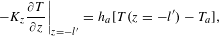 $$\begin{eqnarray}\displaystyle & \displaystyle \left.-K_{z}\frac{\unicode[STIX]{x2202}T}{\unicode[STIX]{x2202}z}\right|_{z=-l^{\prime }}=h_{a}[T(z=-l^{\prime })-T_{a}], & \displaystyle\end{eqnarray}$$
 where  $T_{0}$ and
  $T_{a}$ are the temperatures of the cooling water and surrounding air, respectively;
  $h$ and
  $h_{a}$ are the convective heat transfer coefficients of the heat sink and air, respectively. The parameter
  $h_{a}$ is considered equal to
  $27.5~\text{W}\cdot (\text{m}^{2}\cdot \text{K})^{-1}$ based on Ref. [Reference Xiong, Li, Moore, Huang and Lim24]. The parameters
  $l$ and
  $l^{\prime }$ are the doped crystal thickness and the undoped crystal thickness, respectively.
The solution of Equations (1) and (2) outlines the steady-state temperature distribution in the laser crystal. The high temperature gradient due to a large pump power density in a small pump area will result in a temperature dependent index change, end surface deformation and thermal induced birefringence. Due to its strong intrinsic birefringence, the thermal induced birefringence is small enough to be ignored in the case of Nd:YVO4[Reference Pfistner, Weber, Weber, Merazzi and Gruber26, Reference Tidwell, Seamans, Bowers and Cousins27]. These effects produce a temperature-dependent optical path difference (OPD) in the laser crystal that is given by Ref. [Reference Chen, Kao, Huang, Wang and Wang28] for a crystal with a high-reflectivity end face:
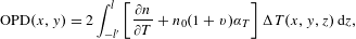 $$\begin{eqnarray}\text{OPD}(x,y)=2\int _{-l^{\prime }}^{l}\left[\frac{\unicode[STIX]{x2202}n}{\unicode[STIX]{x2202}T}+n_{0}(1+\unicode[STIX]{x1D710})\unicode[STIX]{x1D6FC}_{T}\right]\unicode[STIX]{x0394}T(x,y,z)\,\text{d}z,\end{eqnarray}$$
 where  $n$ and
  $n_{0}$ are the refractive indices of the crystal at
  $T$ and room temperature, respectively,
  $\unicode[STIX]{x1D710}=0.33$ is Poisson’s ratio and
  $\unicode[STIX]{x1D6FC}_{T}=4.43\times 10^{-6}~\text{K}^{-1}$ is the thermal expansion coefficient along the
  $z$-axis. The factor 2 in Equation (5) is due to the beam passing through the crystal twice. Ultimately, the
  $\text{OPD}$ changes in crystal transverse correspond to a concave mirror with a radius of curvature
  $R$, which is expressed as follows:
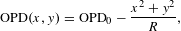 $$\begin{eqnarray}\text{OPD}(x,y)=\text{OPD}_{0}-\frac{x^{2}+y^{2}}{R},\end{eqnarray}$$
 where  $\text{OPD}_{0}$ represents the
  $\text{OPD}$ along the
  $z$-axis
  $(x\,=\,y\,=\,0)$ of the crystal.
2.2 Thermal conductivity
According to Ref. [Reference Ahmadi, Avazpour, Nadgaran and Mousavi29], for Nd:YVO4, the temperature dependence of the thermal conductivity tensor can be written as follows:
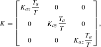 $$\begin{eqnarray}K=\left[\begin{array}{@{}ccc@{}}K_{ax}\displaystyle \frac{T_{a}}{T} & 0 & 0\\ 0 & K_{ay}\displaystyle \frac{T_{a}}{T} & 0\\ 0 & 0 & K_{az}\displaystyle \frac{T_{a}}{T}\end{array}\right],\end{eqnarray}$$
 where  $T$ is the temperature and
  $K_{a}$ is the thermal conductivity coefficient at the specified temperature
  $T_{a}$. For the Nd:YVO4 crystal, the thermal conductivity coefficients in the
  $x$,
$x$,  $y$ and
  $z$ directions are
  $K_{ax}=5.1~\text{W}/(\text{m}\cdot \text{K})$,
  $K_{ay}=5.23~\text{W}/(\text{m}\cdot \text{K})$ and
  $K_{az}=5.1~\text{W}/(\text{m}\cdot \text{K})$ at
  $T_{a}=300~\text{K}$, respectively.
2.3 Fractional thermal loading including ETU effect
In Equation (2),  $\unicode[STIX]{x1D702}_{h}$ is the ratio of thermal load power to absorbed pump power, namely fractional thermal loading, which represents how much absorbed pump power is converted into heat spreading in the crystal. The primary contribution to the thermal loading in Nd:YVO4 comes from the quantum defect, the difference in energy between the pump and laser photons. Moreover, ESA and ETU are the two possible processes that negatively influence laser operation at high population inversion densities. Several publications show that ESA in the Nd ion in most laser crystals at the main laser wavelengths is negligible[Reference Wang, Song, Sun, Xu and Qiu30]. The self-quenching effect, i.e., the cross-relaxation, which was roughly one order of magnitude smaller than the ETU effect, was neglected[Reference Guy, Bonner, Shepherd, Hanna, Tropper and Ferrand31]. The ETU is an energy-transfer process between two neighboring ions in the upper laser level. One ion decays to the lower laser level by transferring its energy to the other ion, which is excited to a higher excited state. The ion in the higher excited state then decays to the upper laser level and the ion in the lower laser level decays to the ground state. These decay processes can be either radiative, nonradiative or a combination of both. The net effect is a reduction in the effective upper laser level lifetime and an increase in fractional thermal loading.
Here we used a rate-equation analysis to investigate the influence of the ETU effects on fractional thermal loading. For an in-band 880 nm pumped Nd:YVO4 laser, referring to the Pollnau and White models[Reference Liu, Fu, Gong and Huang32–Reference Shen, Gong, Ji, Fu and Sun34], we can write the rate equation in laser operation as follows:
 $$\begin{eqnarray}\displaystyle \frac{\text{d}N_{\text{up}}}{\text{d}t}=W_{\text{up}}N_{3}^{2}-\frac{N_{\text{up}}}{\unicode[STIX]{x1D70F}_{\text{up}}}, & & \displaystyle\end{eqnarray}$$
 $$\begin{eqnarray}\displaystyle \frac{\text{d}N_{3}}{\text{d}t} & = & \displaystyle \frac{\unicode[STIX]{x1D706}_{p}\unicode[STIX]{x1D70E}_{\text{abs}}P_{\text{in}}}{hc\unicode[STIX]{x1D70B}\unicode[STIX]{x1D714}_{p}^{2}}N_{1}-\frac{N_{3}}{\unicode[STIX]{x1D70F}_{3}}\nonumber\\ \displaystyle & & \displaystyle -\,2W_{\text{up}}N_{3}^{2}+\frac{N_{\text{up}}}{\unicode[STIX]{x1D70F}_{\text{up}}}-\frac{N_{3}}{hc}\unicode[STIX]{x1D706}_{l}\unicode[STIX]{x1D70E}_{\text{ems}}I_{s},\end{eqnarray}$$
 $$\begin{eqnarray}\displaystyle & \displaystyle \frac{\text{d}N_{2}}{\text{d}t}=-\frac{N_{2}}{\unicode[STIX]{x1D70F}_{2}}+\unicode[STIX]{x1D6FD}_{32}\frac{N_{3}}{\unicode[STIX]{x1D70F}_{3}}+W_{\text{up}}N_{3}^{2}+\frac{N_{3}}{hc}\unicode[STIX]{x1D706}_{l}\unicode[STIX]{x1D70E}_{\text{ems}}I_{s}, & \displaystyle\end{eqnarray}$$
 $$\begin{eqnarray}\displaystyle & \displaystyle \frac{\text{d}N_{1}}{\text{d}t}=-\frac{\unicode[STIX]{x1D706}_{p}\unicode[STIX]{x1D70E}_{\text{abs}}P_{\text{in}}}{hc\unicode[STIX]{x1D70B}\unicode[STIX]{x1D714}_{p}^{2}}N_{1}+\unicode[STIX]{x1D6FD}_{31}\frac{N_{3}}{\unicode[STIX]{x1D70F}_{3}}+\frac{N_{2}}{\unicode[STIX]{x1D70F}_{2}}, & \displaystyle\end{eqnarray}$$
 where  $t$ is the time;
  $N_{i}$ and
  $\unicode[STIX]{x1D70F}_{i}$
 $(i=1,2,3)$ are the population density and fluorescent lifetime of the lowest three energy sublevels, respectively;
  $N_{\text{up}}$ and
  $\unicode[STIX]{x1D70F}_{\text{up}}$ are the population density and lifetime of ETU manifolds, respectively;
  $\unicode[STIX]{x1D6FD}_{3i}$ (
 $i=1,2$) is the fluorescent branching ratio from the upper laser level to the
  $i$th laser level;
  $\unicode[STIX]{x1D706}_{p}$ and
  $\unicode[STIX]{x1D706}_{l}$ are the pump and laser wavelength, respectively;
  $\unicode[STIX]{x1D70E}_{\text{abs}}$ is the absorption cross-section at pump wavelength,
  $\unicode[STIX]{x1D70E}_{\text{ems}}$ is the stimulated emission cross-section,
  $c$ is the speed of light in vacuum,
  $h$ is the Planck constant and
  $W_{\text{up}}$ is the upconversion coefficient. Here we assumed
  $\unicode[STIX]{x1D6FD}_{32}=\unicode[STIX]{x1D6FD}_{31}=0.5$;
  $I_{s}$ is the saturation intensity as follows:
 $$\begin{eqnarray}I_{s}=\frac{hc}{2\unicode[STIX]{x1D706}_{l}\unicode[STIX]{x1D70E}_{\text{ems}}\unicode[STIX]{x1D70F}_{3}}.\end{eqnarray}$$
 The factor 2 in Equation (12) is due to the beam passing through the crystal twice. To take the ETU effect into account, the fractional thermal loading  $\unicode[STIX]{x1D702}_{h}$ can be written as[Reference Bjurshagen and Koch35, Reference Ma, Li, Feng and Zhang36]
 $$\begin{eqnarray}\unicode[STIX]{x1D702}_{h}=\unicode[STIX]{x1D702}+\frac{\unicode[STIX]{x1D706}_{p}}{\unicode[STIX]{x1D706}_{l}}\frac{N_{30}-N_{3}}{N_{30}},\end{eqnarray}$$
 where  $\unicode[STIX]{x1D702}$ is the fractional thermal loading due to quantum defect. The mathematical expression is
  $\unicode[STIX]{x1D702}=1-\unicode[STIX]{x1D706}_{p}/\unicode[STIX]{x1D706}_{l}$.
  $N_{30}$ is the population in the upper laser level without the ETU effect and
  $N_{3}$ is the population in the upper laser level considering the influence of the ETU effect.
3 Experimental setup
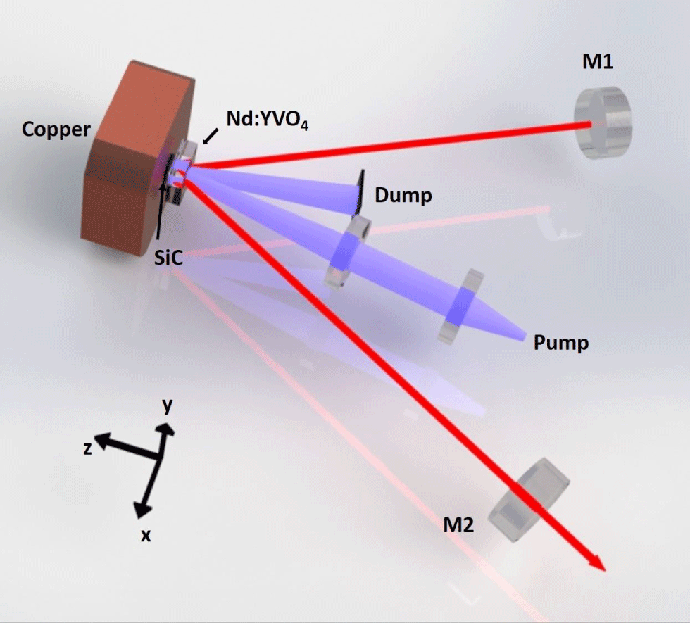
Figure 2. Schematic of the experimental setup.
The experimental setup of the double-pass pumped Nd:YVO4 thin disk laser is shown in Figure 2. Two types of  $a$-cut Nd:YVO4 crystals were used including a
  $15~\text{mm}\times 15~\text{mm}\times (4+0.5)~\text{mm}$ single diffusion bonded YVO4-Nd:YVO4 with 1 at.% doping concentration and a
  $15~\text{mm}\times 15~\text{mm}\times (4+1)~\text{mm}$ single diffusion bonded YVO4-Nd:YVO4 with 0.5 at.% doping concentration. The thickness of YVO4 was 4 mm in both crystals. The thickness of Nd:YVO4 was 0.5 mm of 1 at.% doped crystal and 1 mm of 0.5 at.% doped crystal. The undoped end face of the crystal was anti-reflection-coated at both 880 and 1064 nm. At the same time, the doped end face of the crystal was high-reflection-coated at both 880 and 1064 nm. The crystal was mounted tightly with the water-cooled heat sinks using a copper tablet (not shown in Figure 2). The
  $c$-axis of the crystal was aligned with the
  $y$-axis (perpendicular to the working plane). The entire heat sink system consisted of a water-cooled copper block and a SiC crystal. The diameter of the SiC crystal was 15 mm and the thickness was 2 mm. Two 0.2 mm thick indium foils were placed between the copper, the SiC crystal and the doped end face of the Nd:YVO4 crystal to ensure optimal thermal contact. The chiller temperature was maintained at
  $20\,^{\circ }\text{C}$ during laser operation. The pump source was a fiber-coupled laser diode, for which the wavelength was fixed at 880 nm. This can deliver a maximum pump power of 100 W through a 2 m long fiber. The fiber had a core diameter of
  $200~\unicode[STIX]{x03BC}\text{m}$ and a numerical aperture of 0.22. The pump light was imaged to a 1.1 mm diameter spot at the undoped end face of the crystal by coupling optics, providing an almost collimated pump volume along the entire crystal thickness. The unabsorbed pump power was collected into the dump.
The cavity was formed by two plane mirrors M1 and M2. Mirror M1 was high-reflection-coated at 1064 nm ( $R>99.95\%$). Mirror M2 was used as the output coupler with 30% output coupling efficiency. The distance between M1 and the crystal was 150 mm; the distance between M2 and the crystal was the same.
4 Experimental and numerical analysis results
The output performance of the diode double-pass pumped Nd:YVO4 thin disk laser was affected by thermal effects. First, the CW output power of the Nd:YVO4 thin disk laser was tested. A symmetrical V-type cavity was used. At the same time, a portable thermometer was used to detect the temperature at the center of the undoped end face of the crystal. In this configuration, the curves of the output power and center temperature of the undoped end face of the crystal versus the absorbed pump power are shown in Figures 3(a) and 3(b) for 1 at.% doped and 0.5 at.% doped Nd:YVO4 lasers, respectively.
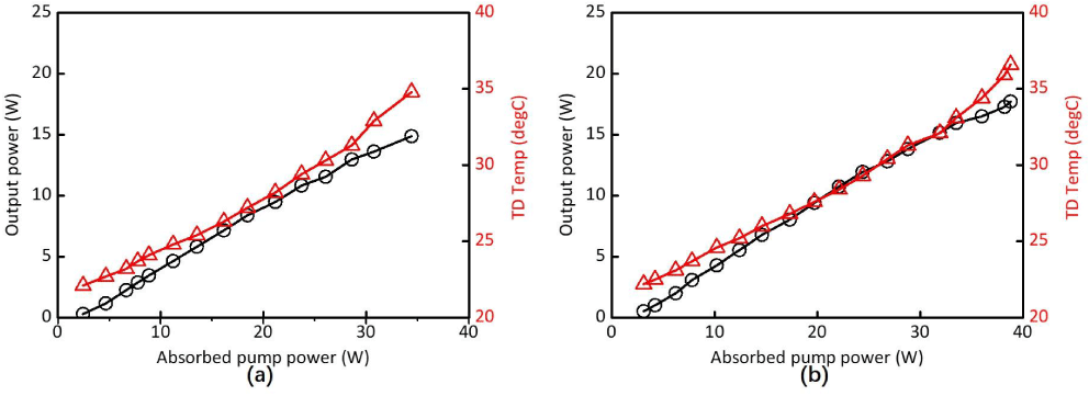
Figure 3. Output power and thin disk (TD) temperature versus absorbed pump power of (a) 1 at.% doped and (b) 0.5 at.% doped systems.
As shown in Figure 3(a), both the output power and the center temperature of the undoped end face of the crystal increased linearly with increasing absorbed pump power for the 1 at.% doped system. The maximum output power of 14.87 W was achieved at an absorbed pump power of 34.4 W, so the optical-to-optical efficiency relative to absorbed pump power was calculated to be 43%. The pump absorption efficiency at the maximum output power was measured to be 51.7%. The highest temperature at the center of the undoped end face of the crystal reached  $34.8\,^{\circ }\text{C}$ at the maximum output power. If we continue to increase the input pump power, the output power will drop sharply or even disappear, indicating that the entire system had been running at the edge of the stable range when the output power reached the maximum due to the thermal lens effect of the laser crystal. According to the ABCD transmission matrix and the stability conditions of the cavity, the equivalent radius of curvature of the laser crystal was about 150 mm at maximum output power.
As shown in Figure 3(b), the output power and the temperature at the center of the undoped end face of the crystal varying with the absorbed pump power exhibited the same tendency as shown in Figure 3(a) for the 0.5 at.% doped system. However, the difference was that the highest output power reached 17.71 W when the absorbed pump power was 38.8 W. Therefore, the optical-to-optical efficiency relative to absorbed pump power was calculated to be 46%. The measured pump light absorption efficiency in this condition was 47%. Moreover, when the maximum output power was reached, the temperature at the center of the undoped end face of the crystal was  $36.6\,^{\circ }\text{C}$ higher than the maximum temperature in Figure 3(a). As in the 1 at.% doped system, the equivalent radius of curvature of the concave mirror, produced by the thermal effect in the laser crystal in this condition, was approximately 150 mm. This is the critical value of the stable range. Figure 3 shows that the 0.5 at.% doped crystals can withstand higher absorbed pump power under the same critical conditions for higher output power. Furthermore, at maximum output power, the maximum temperature of the undoped end face center of the 0.5 at.% doped system was higher than that of the 1 at.% doped system.
In addition to the output power, output beam quality was also an important indicator of the output performance of the thin disk laser. The output beam quality of different doped systems was observed with the same cavity. We placed a charge-coupled device camera behind the mirror M1 and monitored the beam profile of the system by measuring the light leakage behind the mirror M1. The beam profiles of different doped systems at different absorbed pump powers are shown in Figures 4 and 5. As shown in Figure 4, the output beam profile evolved from the fundamental mode to the multimode with increasing absorbed pump power for the 1 at.% doped system. When the absorbed pump power was no more than 8.3 W, the output mode was the fundamental mode as shown in Figure 4(a). Further increasing the pump power, the output beam quality began to deteriorate, and the center of the output spot profile began to split as shown in Figure 4(b). After that, as the absorbed pump power further increased, the beam profile turned into a multimode operation as shown in Figures 4(c) and 4(d). When the absorbed pump power reached 34.4 W, the maximum output power of 14.87 W was reached, and the beam profile was similar to the profile of the fundamental mode. Detailed characteristics of the beam profile at maximum output power were confirmed by measuring the  $M^{2}$ factor. Typical beam quality data are shown in Figure 6 and measured
  $M^{2}$ factors are
  $M_{x}^{2}=1.04$ and
  $M_{y}^{2}=1.74$ in the
  $x$-axis and
  $y$-axis directions. Near-field and far-field beam profiles are shown in the insets of Figure 6. The result confirmed that the maximum output was a slight multimode operation.
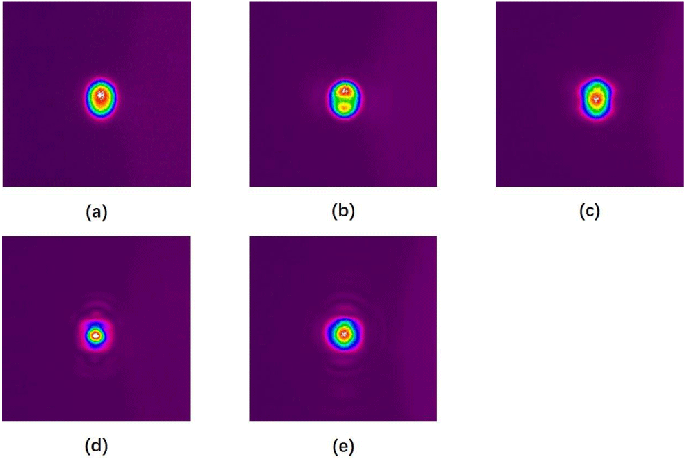
Figure 4. Beam profiles of 1 at.% doped system at different absorbed pump powers: (a) 8.3 W, (b) 18.5 W, (c) 23.7 W, (d) 28.6 W and (e) 34.4 W.
Figure 5. Beam profiles of 0.5 at.% doped system at different absorbed pump powers: (a) 9.1 W, (b) 18.5 W, (c) 24.4 W, (d) 28.8 W, (e) 34.7 W and (f) 38.8 W.
Figure 6. Output beam quality. Near-field beam profile (upper left) and far-field beam profile (upper right).
In contrast, the output beam profile of the 0.5 at.% doped system had an evolution similar to that of the 1 at.% doped system, with a slightly different turning point. Figure 5 illustrates the beam profile of the 0.5 at.% doped system at different absorbed pump powers. As shown in Figure 5(a), the output mode was the fundamental mode when the absorbed power was no more than 9.1 W. Then, as the absorbed pump power increased, the output beam profile center began to gradually disperse and transform into a multimode operation, as shown in Figures 5(b)–5(e). Figure 5(f) illustrates the beam profile at the maximum output power of 17.71 W with an absorbed pump power of 38.8 W. It was obvious that the system at this time was in multimode operation. Figures 4 and 5 show that the 0.5 at.% doped system can maintain the fundamental mode operation while absorbing higher pump power before it changes into a multimode for the first time. However, the 1 at.% doped system had better beam quality at maximum output power. On the one hand, the resonator runs in a critical state of stability conditions and is extremely sensitive to the equivalent radius of curvature of the crystal at maximum output power. On the other hand, there may be some quality differences between the two types of crystals, which will in turn affect the characteristics of the output beam. The optimization of the output mode is not performed here because the purpose of this study is to compare the effects of different crystal thicknesses and doping concentrations on the thermal performance of the double-pass pumped Nd:YVO4 thin disk laser.
The numerical analysis was based on the finite-element method through the COMSOL Multiphysics software and MATLAB. A three-dimensional model was used for numerical analysis. According to the design of the heat dissipation system, we assumed that the temperature of the copper heat sink was equal to the temperature of the cooling water and the ambient temperature  $T_{a}$ was
  $22.5\,^{\circ }\text{C}$. From our measured absorption efficiency
  $\unicode[STIX]{x1D6FE}$ of 1 at.% and 0.5 at.% doped crystals, we can conclude that the absorption coefficients
  $\unicode[STIX]{x1D6FC}$ were
  $7.2774~\text{cm}^{-1}$ and
  $3.1744~\text{cm}^{-1}$, respectively. In theory, the absorption coefficient was proportional to the doping concentration. The measured absorption coefficient of the 0.5 at.% doped crystal was smaller than half of the absorption coefficient of the 1 at.% doped crystal because the doping concentration and thickness of the crystal had certain processing errors. The parameter
  $\unicode[STIX]{x1D702}_{h}$ can be solved through Equation (13) as described in Section 2.3. The absorption cross-section can be derived from the absorption coefficient and the doping concentration. We assumed that
  $\unicode[STIX]{x1D70F}_{\text{up}}$ and
  $\unicode[STIX]{x1D70F}_{2}$ were
  $0.5~\unicode[STIX]{x03BC}\text{s}$, which equals the calculated step size. According to Ref. [Reference Chen, Lee, Huang and Wang37], the
  $\unicode[STIX]{x1D70F}_{3}$ values for 1 at.% and 0.5 at.% doped crystals were
  $83~\unicode[STIX]{x03BC}\text{s}$ and
  $95~\unicode[STIX]{x03BC}\text{s}$, respectively. According to Ref. [Reference Cante, Beecher and Mackenzie38], the upconversion coefficient
  $W_{\text{up}}$ decreased when the temperature increased while the doping concentration remained constant. Therefore, we took values of
  $W_{\text{up}}$, which equaled
  $2.4\times 10^{-16}~\text{cm}^{3}/\text{s}$ and
  $0.3\times 10^{-16}~\text{cm}^{3}/\text{s}$ for 1 at.% and 0.5 at.% doped crystals, respectively. The upconversion coefficient
  $W_{\text{up}}$ is obtained by fitting the experimental data, which is different from the literature[Reference Shen, Gong, Ji, Fu and Sun34, Reference Chen, Lee, Huang and Wang37–Reference Délen, Balembois, Musset and Georges39]. The fourth-order Runge–Kutta method is used to solve Equations (8)–(11). The parameters
  $N_{3}$ and
  $N_{30}$ can be obtained, corresponding to the cases with and without the ETU, respectively, and then substituted into Equation (13). The fractional thermal loading
  $\unicode[STIX]{x1D702}_{h}$ can be calculated as
  $0.26$ and
  $0.18$ for 1 at.% and 0.5 at.% doped crystals, respectively. This made it possible to calculate the temperature distribution in the crystal using the theoretical model mentioned in Section 2.1, while considering the temperature-dependent thermal conductivity tensor and the influence of the ETU effect.
Figure 7. Two-dimensional temperature distributions of the undoped end face of the crystal at the maximum output power in simulations of (a) 1 at.% doped and (b) 0.5 at.% doped systems.
The two-dimensional temperature distributions of the undoped end face of the 1 at.% doped crystal with  $P_{\text{in}}=66.5~\text{W}$ and 0.5 at.% doped crystal with
  $P_{\text{in}}=82.4~\text{W}$ are shown in Figures 7(a) and 7(b), respectively. As the figure shows, the maximum temperatures of the undoped end face of the crystal were
  $30.9667\,^{\circ }\text{C}$ and
  $32.4692\,^{\circ }\text{C}$ for the 1 at.% and 0.5 at.% doped systems, respectively. The temperature distribution was asymmetrical because the thermal conductivity along
  $x$-axis and
  $y$-axis directions was different. The temperature distributions along the
  $x$-axis and
  $y$-axis on the undoped end face of the crystal of 1 at.% and 0.5 at.% doped systems are shown in Figures 8(a) and 8(b), respectively. It can be seen that the temperature in the
  $y$-axis direction was slightly higher than the temperature in the
  $x$-axis direction due to the difference in thermal conductivity between the two axial directions in Figures 8(a) and 8(b).
Figure 8. Temperature distributions along with the undoped end face of (a) 1 at.% doped and (b) 0.5 at.% doped systems; the central axes of (c) 1 at.% doped and (d) 0.5 at.% doped systems.
To gain a better understanding of how an undoped end cap can be used to relieve thermal effects, we plotted temperature changes in the central axis of two different doped systems with the  $z=0$ plane located on the pump absorbed plane in Figures 8(c) and 8(d). The coordinate zero point represents the interface between the doped and undoped parts of the crystal. The
  $z=l$ location represents the doped end face of the crystal, which was cooled by the heat sink system. The
  $z=-l^{\prime }$ location represents the undoped end face of the crystal. In both two conditions, the temperature rose from the pumped surfaces and achieved maximum values at the adjacent junction between the doped parts and undoped caps of composite crystals. It can be seen that the maximum temperatures were
  $231\,^{\circ }\text{C}$ and
  $198\,^{\circ }\text{C}$ for 1 at.% and 0.5 at.% doped systems, respectively.
Based on the temperature field distribution of the crystal (calculated previously) and the theoretical model in Section 2.1, we can further calculate the equivalent radius of curvature for the crystal formed by the uneven temperature distribution. The calculated results of the total thermally induced OPD changes along the  $y$-axis for 1 at.% and 0.5 at.% doped systems (referring to Equation (5)) are shown in Figures 9(a) and 9(b), respectively. To deduce the equivalent radius of curvature of the crystal, we fitted the data using Equation (6) in the pump area. The fitting results are shown in Figures 9(c) and 9(d) for 1 at.% and 0.5 at.% doped systems, respectively. The simulated data are shown as discrete points in Figures 9(c) and 9(d). The equivalent radii of curvature of the crystal obtained by fitting were 157 mm and 154 mm according to Figures 9(a) and 9(b) for 1 at.% and 0.5 at.% doped systems, respectively. The equivalent radius of curvature of the crystal obtained by numerical analysis was close to the experimental critical radius of curvature, which verifies the accuracy of our theoretical model. The results of the above numerical analysis and experimental study indicated that the 0.5 at.% doped system can withstand a higher absorbed pump power than the 1 at.% doped system to achieve a higher power output at the same critical cavity length. The fractional thermal loading of the 1 at.% doped system was higher than that of the 0.5 at.% doped system due to the influence of the ETU effect. In addition, the doped layer of the 1 at.% doped system was thinner and therefore had a better heat dissipation performance. Thus, the 0.5 at.% doped system had higher output power and efficiency, but the 1 at.% doped system had better output beam quality at the maximum output power. Therefore, the 0.5 mm thick 1 at.% doped system was more suitable for achieving high power and good beam quality for the double-pass pumped Nd:YVO4 thin disk laser, but a more effective heat dissipation system design, such as heat sinks made of diamond, is necessary to further mitigate the influence of the ETU effect on thermal load. Besides, polarization pumping can be used to improve the total optical-to-optical efficiency of the double-pass pumped Nd:YVO4 thin disk laser.
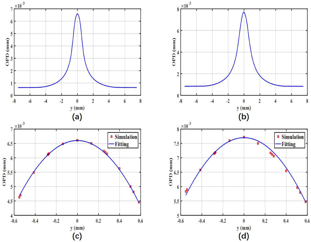
Figure 9. Thermal induced OPDs of (a) 1 at.% doped and (b) 0.5 at.% doped systems; equivalent radii of curvature fitting of (c) 1 at.% doped and (d) 0.5 at.% doped systems.
5 Conclusion
In summary, we demonstrated a simple, compact double-pass pumped Nd:YVO4 thin disk laser. The schemes of in-band pumping, undoped end face bonds and SiC material heat sink were combined to alleviate the thermal effects. The CW performances of the double-pass pumped Nd:YVO4 thin disk laser with different doping concentrations and thicknesses were investigated experimentally. The maximum CW output power of 17.71 W with an optical-to-optical efficiency relative to absorbed pump power of 46% was obtained by the 0.5 at.% doped composite crystal under an absorbed pump power of 38.8 W. In addition, a maximum CW output power of 14.87 W with an optical-to-optical efficiency relative to an absorbed pump power of 43% was obtained by the 1 at.% doped composite crystal under an absorbed pump power of 34.4 W. Furthermore, the output beam characteristics of different doped systems were compared. The 0.5 at.% doped system had a higher output power and efficiency, but the 1 at.% doped system had a better output beam quality at the maximum output power. Numerical analysis and experimental study of the temperature distribution and thermal lens effect in the double-pass pumped Nd:YVO4 thin disk laser were also presented considering the influence of the ETU effects and the temperature dependence of the thermal conductivity tensor. The simulation and experiment results were in good agreement. Moreover, both experiment and simulation results indicated that the fractional thermal loading of the 1 at.% doped system increased to 0.26 while it only increased to 0.18 for the 0.5 at.% doped system due to the influence of the ETU effect. Consequently, the theoretical model can be employed as a useful tool for the design of the distributed face cooling scheme.
Funding
Ministry of Science and Technology of the People’s Republic of China (MOST) (2016YFB1102402, 2017YFB0405202); Key Laboratory of Opto-electronic Information Technology, Ministry of Education (Tianjin University), China (2019KFKT003); Shanghai Science and Technology Achievements Transformation and Industrialization project (18511109800).


 Open access