
Hierarchical NiO/CMK-3 Photocathode for a p-Type Dye-Sensitized Solar Cell with Improved Photoelectrochemical Performance and Fast Hole Transfer

 and
and
Abstract
:1. Introduction
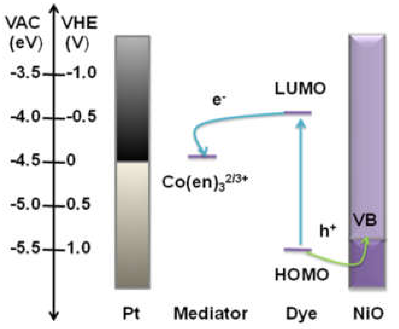
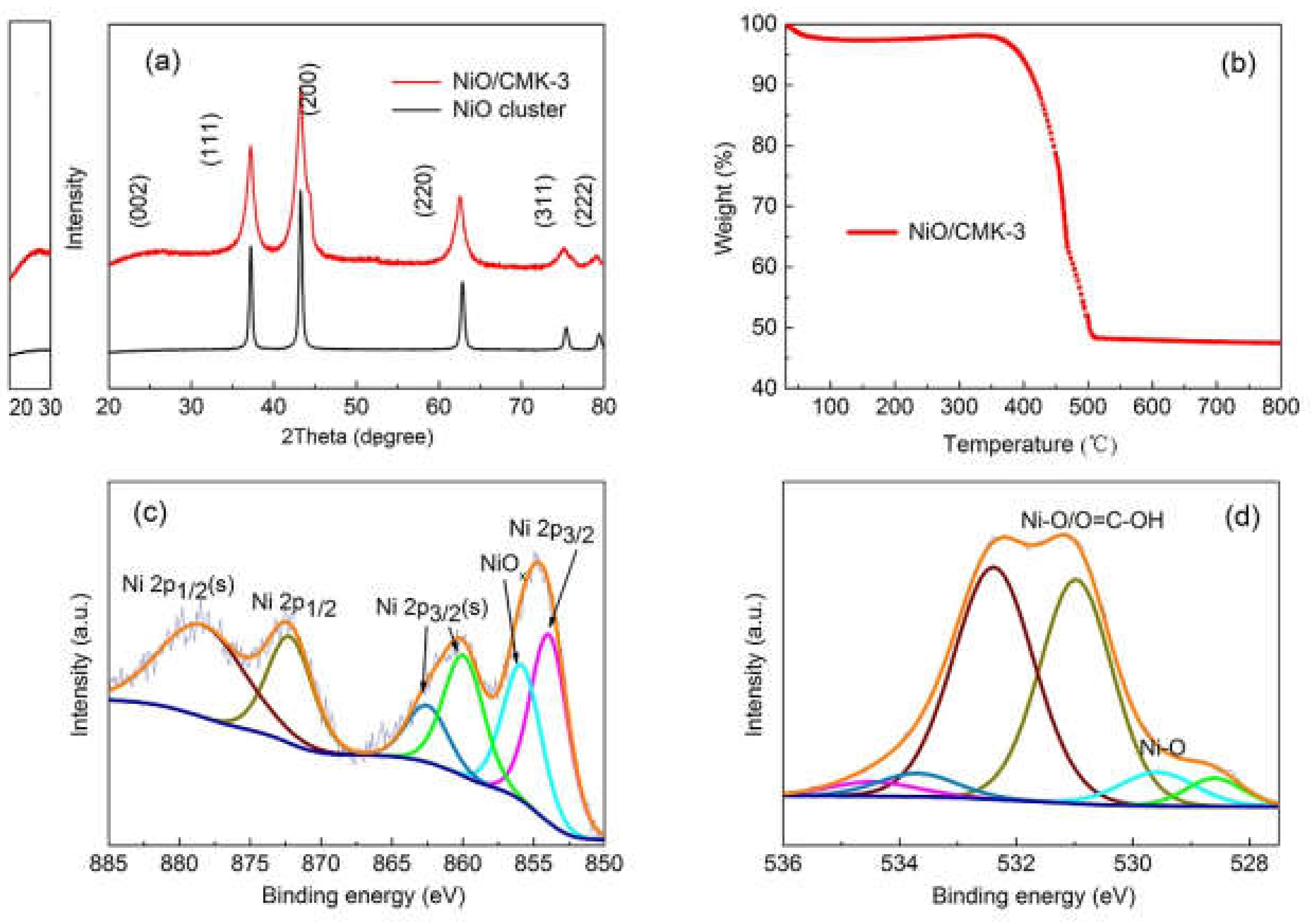
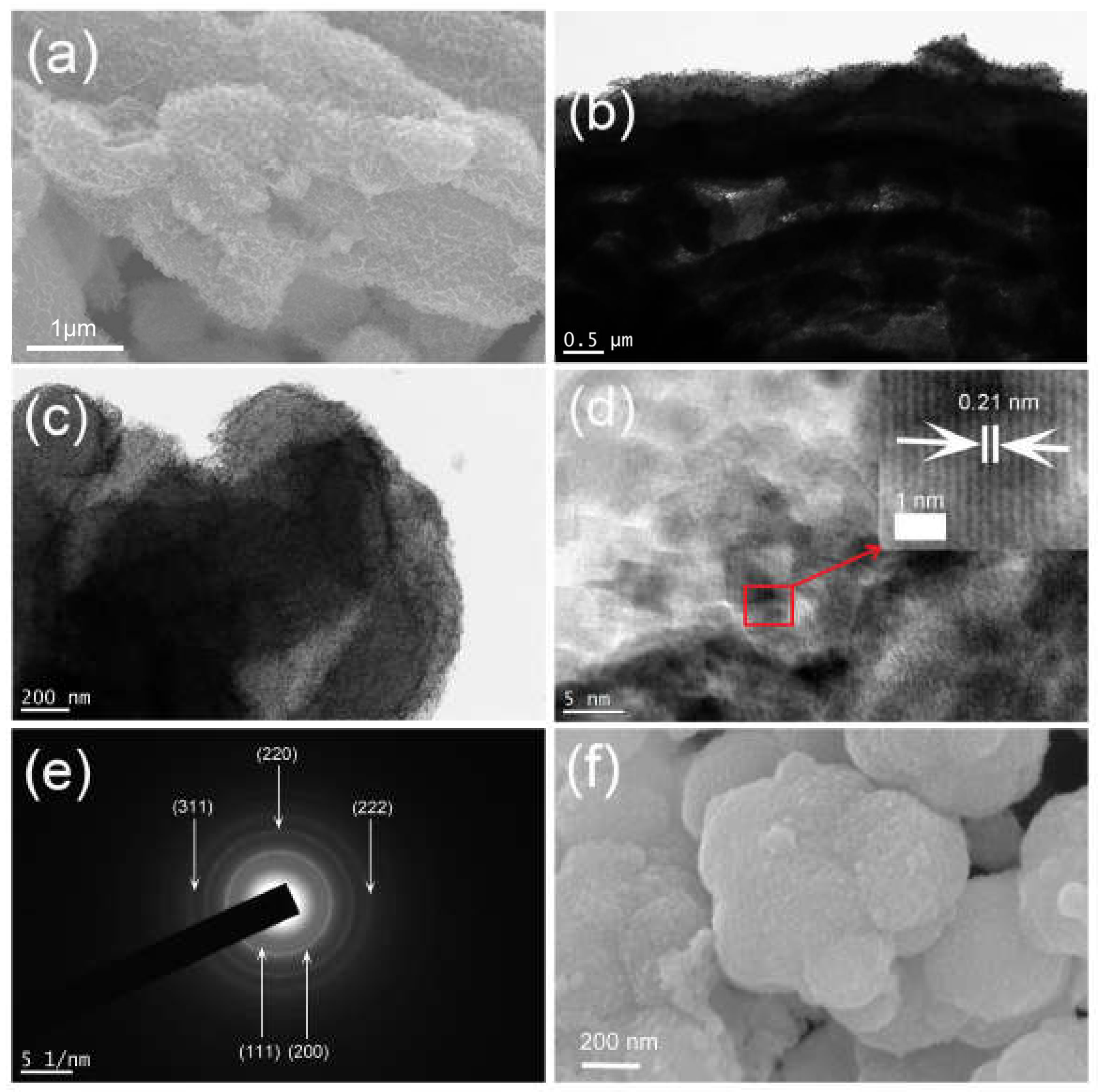
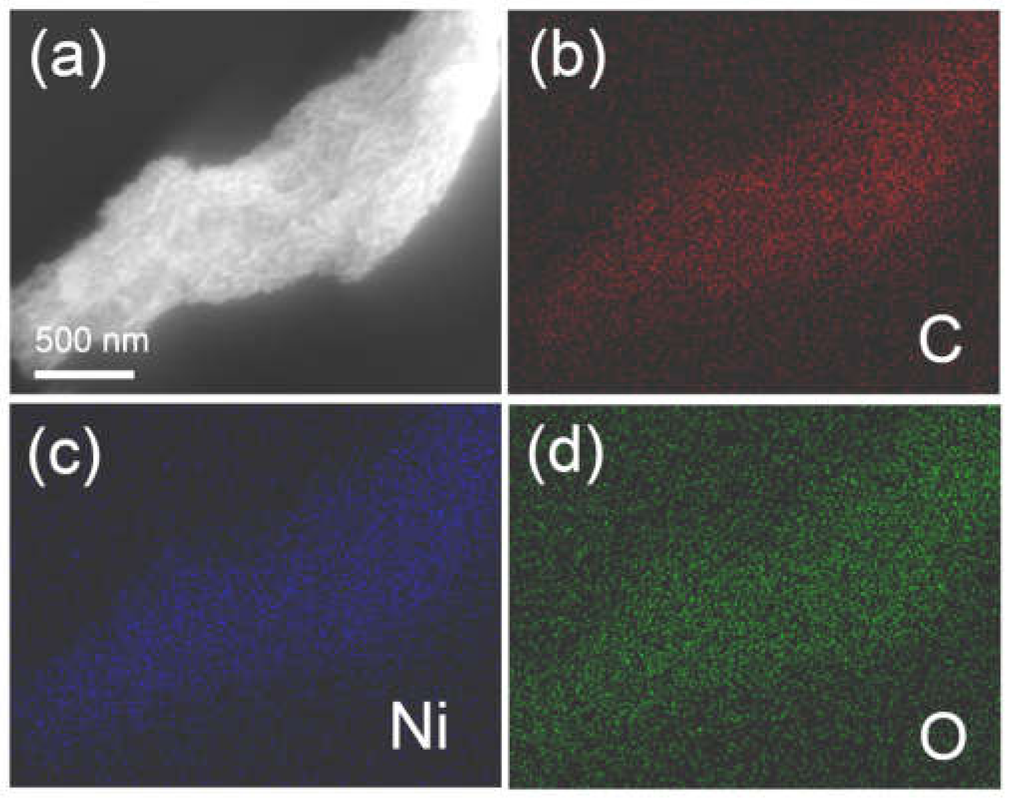
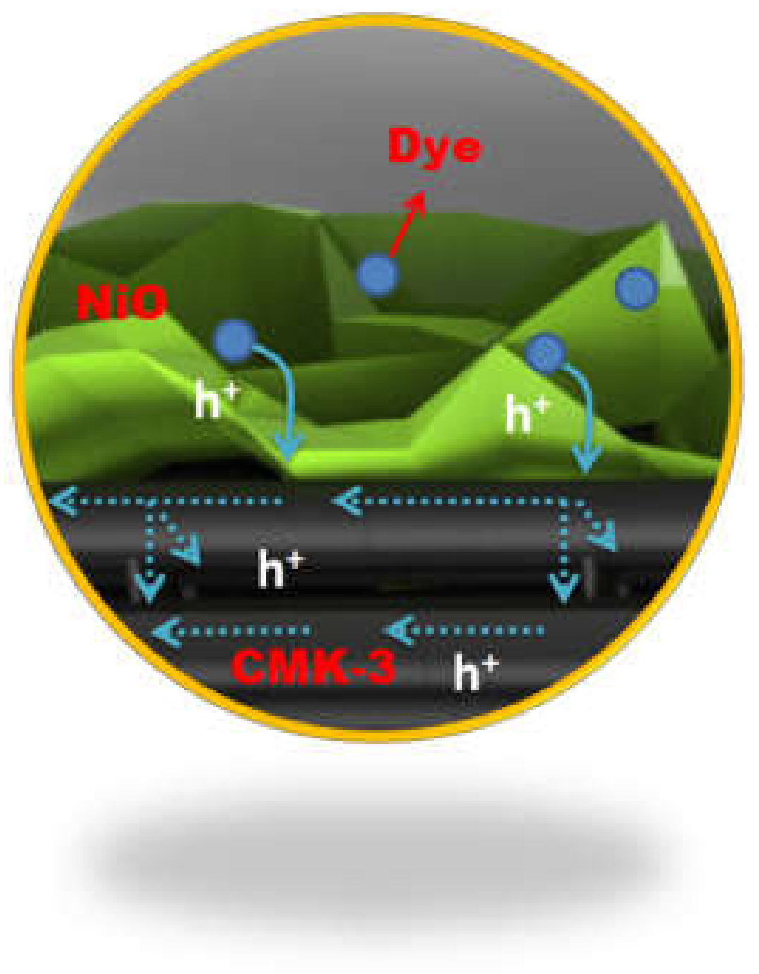
2. Results
3. Discussion
4. Materials and Methods
4.1. Preparation of Hierarchical NiO/CMK-3 Nanocomposite and NiO Clusters
4.2. Materials Characterization
4.3. Preparation of the NiO and NiO/CMK-3 Films
4.4. Fabrication and Characterization of the p-DSSC Devices
5. Conclusions
Supplementary Materials
Author Contributions
Funding
Conflicts of Interest
References
- Yella, A.; Lee, H.-W.; Tsao, H.N.; Yi, C.; Chandiran, A.K.; Nazeeruddin, M.K.; Diau, E.W.-G.; Yeh, C.-Y.; Zakeeruddin, S.M.; Grätzel, M. Porphyrin-sensitized solar cells with cobalt (II/III)–based redox electrolyte exceed 12 percent efficiency. Science 2011, 334, 629–634. [Google Scholar] [CrossRef] [PubMed]
- Tan, R.; Wei, Z.; Liang, J.; Lv, Z.; Chen, B.; Qu, J.; Yan, W.; Ma, J. Enhanced open-circuit photovoltage and charge collection realized in pearl-like NiO/CuO composite nanowires based p-type dye sensitized solar cells. Mater. Res. Bull. 2019, 116, 131–136. [Google Scholar] [CrossRef]
- Bakker, T.M.; Mathew, S.; Reek, J.N. Lindqvist polyoxometalates as electrolytes in p-type dye sensitized solar cells. Sustain. Energ. Fuels 2019, 3, 96–100. [Google Scholar] [CrossRef]
- Sen, A.; Groß, A. Does Involving Additional Linker Always Increase the Efficiency of an Organic Dye for p-Type Dye-Sensitized Solar Cells? ACS Appl. Energy Mater. 2019, 2, 6341–6347. [Google Scholar] [CrossRef]
- Langmar, O.; Fazio, E.; Schol, P.; de la Torre, G.; Costa, R.D.; Torres, T.; Guldi, D.M. Controlling Interfacial Charge Transfer and Fill Factors in CuO-based Tandem Dye-Sensitized Solar Cells. Angew. Chem. Int. Ed. 2019, 58, 4056–4060. [Google Scholar] [CrossRef]
- Nattestad, A.; Mozer, A.J.; Fischer, M.K.; Cheng, Y.-B.; Mishra, A.; Bäuerle, P.; Bach, U. Highly efficient photocathodes for dye-sensitized tandem solar cells. Nat. Mater. 2010, 9, 31–35. [Google Scholar] [CrossRef]
- Odobel, F.; Le Pleux, L.; Pellegrin, Y.; Blart, E. New photovoltaic devices based on the sensitization of p-type semiconductors: Challenges and opportunities. Acc. Chem. Res. 2010, 43, 1063–1071. [Google Scholar] [CrossRef]
- Gong, J.; Sumathy, K.; Qiao, Q.; Zhou, Z. Review on dye-sensitized solar cells (DSSCs): Advanced techniques and research trends. Renew. Sust. Energ. Rev. 2017, 68, 234–246. [Google Scholar] [CrossRef]
- Wood, C.J.; Summers, G.H.; Clark, C.A.; Kaeffer, N.; Braeutigam, M.; Carbone, L.R.; d’Amario, L.; Fan, K.; Farré, Y.; Narbey, S. A comprehensive comparison of dye-sensitized NiO photocathodes for solar energy conversion. Phys. Chem. Chem. Phys. 2016, 18, 10727–10738. [Google Scholar] [CrossRef] [Green Version]
- Brisse, R.; Faddoul, R.; Bourgeteau, T.; Tondelier, D.; Leroy, J.; Campidelli, S.; Berthelot, T.; Geffroy, B.; Jousselme, B. Inkjet printing NiO-based p-type dye-sensitized solar cells. ACS Appl. Mater. Inter. 2017, 9, 2369–2377. [Google Scholar] [CrossRef]
- Bonomo, M.; Di Girolamo, D.; Piccinni, M.; Dowling, D.P.; Dini, D. Electrochemically Deposited NiO Films as a Blocking Layer in p-Type Dye-Sensitized Solar Cells with an Impressive 45% Fill Factor. Nanomaterials 2020, 10, 167. [Google Scholar] [CrossRef] [PubMed] [Green Version]
- Bonomo, M.; Dini, D.; Decker, F. Electrochemical and photoelectrochemical properties of nickel oxide (NiO) with nanostructured morphology for photoconversion applications. Front. Chem. 2018, 6, 601. [Google Scholar] [CrossRef] [PubMed]
- Awais, M.; Gibson, E.; Vos, J.G.; Dowling, D.P.; Hagfeldt, A.; Dini, D. Fabrication of Efficient NiO Photocathodes Prepared via RDS with Novel Routes of Substrate Processing for p-Type Dye-Sensitized Solar Cells. Chem Electro. Chem 2014, 1, 384–391. [Google Scholar] [CrossRef]
- Liu, Q.; Wei, L.; Yuan, S.; Ren, X.; Zhao, Y.; Wang, Z.; Zhang, M.; Shi, L.; Li, D.; Li, A. Influence of interface properties on charge density, band edge shifts and kinetics of the photoelectrochemical process in p-type NiO photocathodes. RSC Adv. 2015, 5, 71778–71784. [Google Scholar] [CrossRef]
- Odobel, F.; Pellegrin, Y. Recent advances in the sensitization of wide-band-gap nanostructured p-type semiconductors. Photovoltaic and photocatalytic applications. J. Phys. Chem. Lett. 2013, 4, 2551–2564. [Google Scholar] [CrossRef]
- Muñoz-Garcia, A.B.; Caputo, L.; Schiavo, E.; Baiano, C.; Maddalena, P.; Pavone, M. Ab initio study of anchoring groups for CuGaO2 delafossite-based p-type dye sensitized solar cells. Front. Chem. 2019, 7, 158. [Google Scholar] [CrossRef] [Green Version]
- Jiang, T.; Bujoli-Doeuff, M.; Farré, Y.; Pellegrin, Y.; Gautron, E.; Boujtita, M.; Cario, L.; Jobic, S.; Odobel, F. CuO nanomaterials for p-type dye-sensitized solar cells. RSC Adv. 2016, 6, 112765–112770. [Google Scholar] [CrossRef]
- D’Amario, L.; Antila, L.J.; Pettersson Rimgard, B.; Boschloo, G.; Hammarström, L. Kinetic evidence of two pathways for charge recombination in NiO-based dye-sensitized solar cells. J. Phys. Chem. Lett. 2015, 6, 779–783. [Google Scholar] [CrossRef]
- Yang, H.; Guai, G.H.; Guo, C.; Song, Q.; Jiang, S.P.; Wang, Y.; Zhang, W.; Li, C.M. NiO/graphene composite for enhanced charge separation and collection in p-type dye sensitized solar cell. J. Phys. Chem. C 2011, 115, 12209–12215. [Google Scholar] [CrossRef]
- Powar, S.; Wu, Q.; Weidelener, M.; Nattestad, A.; Hu, Z.; Mishra, A.; Bäuerle, P.; Spiccia, L.; Cheng, Y.-B.; Bach, U. Improved photocurrents for p-type dye-sensitized solar cells using nano-structured nickel (II) oxide microballs. Energ. Environ. Sci. 2012, 5, 8896–8900. [Google Scholar] [CrossRef]
- Fan, Z.; Liang, J.; Yu, W.; Ding, S.; Cheng, S.; Yang, G.; Wang, Y.; Xi, Y.; Xi, K.; Kumar, R.V. Ultrathin NiO nanosheets anchored on a highly ordered nanostructured carbon as an enhanced anode material for lithium ion batteries. Nano Energy 2015, 16, 152–162. [Google Scholar] [CrossRef]
- Qu, J.; Yang, Y.; Shi, X.; Wang, W.; Ding, J.; Yuan, N.; Zhao, X.; Lai, C. Scalable synthesis of ultrasmall SnO2 nanocrystals in carbon conductive matrices: High loading and excellent electrochemical performance. J. Alloy. Compd. 2016, 686, 122–129. [Google Scholar] [CrossRef]
- Wang, Y.; Rho, W.-Y.; Yang, H.-Y.; Mahmoudi, T.; Seo, S.; Lee, D.-H.; Hahn, Y.-B. Air-stable, hole-conductor-free high photocurrent perovskite solar cells with CH3NH3PbI3-NiO nanoparticles composite. Nano Energy 2016, 27, 535–544. [Google Scholar] [CrossRef]
- Park, J.H.; Seo, J.; Park, S.; Shin, S.S.; Kim, Y.C.; Jeon, N.J.; Shin, H.W.; Ahn, T.K.; Noh, J.H.; Yoon, S.C. Efficient CH3NH3PbI3 perovskite solar cells employing nanostructured p-type NiO electrode formed by a pulsed laser deposition. Adv. Mater. 2015, 27, 4013–4019. [Google Scholar] [CrossRef]
- Seo, S.; Park, I.J.; Kim, M.; Lee, S.; Bae, C.; Jung, H.S.; Park, N.-G.; Kim, J.Y.; Shin, H. An ultra-thin, un-doped NiO hole transporting layer of highly efficient (16.4%) organic–inorganic hybrid perovskite solar cells. Nanoscale 2016, 8, 11403–11412. [Google Scholar] [CrossRef]
- Kwon, U.; Kim, B.-G.; Nguyen, D.C.; Park, J.-H.; Ha, N.Y.; Kim, S.-J.; Ko, S.H.; Lee, S.; Lee, D.; Park, H.J. Solution-processible crystalline NiO nanoparticles for high-performance planar perovskite photovoltaic cells. Sci. Rep. 2016, 6, 30759. [Google Scholar] [CrossRef] [Green Version]
- Zhao, B.; Ke, X.-K.; Bao, J.-H.; Wang, C.-L.; Dong, L.; Chen, Y.-W.; Chen, H.-L. Synthesis of flower-like NiO and effects of morphology on its catalytic properties. J. Phys. Chem. C 2009, 113, 14440–14447. [Google Scholar] [CrossRef]
- Langell, M.; Nassir, M. Stabilization of NiO (111) thin films by surface hydroxyls. J. Phys. Chem. 1995, 99, 4162–4169. [Google Scholar] [CrossRef]
- Mrowec, S.; Grzesik, Z. Oxidation of nickel and transport properties of nickel oxide. J. Phys. Chem. Solids 2004, 65, 1651–1657. [Google Scholar] [CrossRef]
- Uhlenbrock, S.; Scharfschwerdt, C.; Neumann, M.; Illing, G.; Freund, H.-J. The influence of defects on the Ni 2p and O 1s XPS of NiO. J. Phys.: Condens. Matter 1992, 4, 7973–7978. [Google Scholar] [CrossRef]
- Abdelkader, A.; Fray, D. Controlled electrochemical doping of graphene-based 3D nanoarchitecture electrodes for supercapacitors and capacitive deionisation. Nanoscale 2017, 9, 14548–14557. [Google Scholar] [CrossRef] [PubMed]
- Wang, Y.; Zheng, X.; Qu, Q.; Liu, G.; Battglia, V.S.; Zheng, H. A novel maleic acid/graphite composite anode for lithium ion batteries with high energy and power density. Carbon 2018, 132, 420–429. [Google Scholar] [CrossRef]
- Xu, X.; Tan, H.; Xi, K.; Ding, S.; Yu, D.; Cheng, S.; Yang, G.; Peng, X.; Fakeeh, A.; Kumar, R.V. Bamboo-like amorphous carbon nanotubes clad in ultrathin nickel oxide nanosheets for lithium-ion battery electrodes with long cycle life. Carbon 2015, 84, 491–499. [Google Scholar] [CrossRef]
- Li, L.; Gibson, E.A.; Qin, P.; Boschloo, G.; Gorlov, M.; Hagfeldt, A.; Sun, L. Double-layered NiO photocathodes for p-type DSSCs with record IPCE. Adv. Mater. 2010, 22, 1759–1762. [Google Scholar] [CrossRef]
- Zannotti, M.; Wood, C.J.; Summers, G.H.; Stevens, L.A.; Hall, M.R.; Snape, C.E.; Giovanetti, R.; Gibson, E.A. Ni Mg mixed metal oxides for p-type dye-sensitized solar cells. ACS Appl. Mater. Inter. 2015, 7, 24556–24565. [Google Scholar] [CrossRef] [Green Version]
- Zhang, X.L.; Zhang, Z.; Chen, D.; Bäuerle, P.; Bach, U.; Cheng, Y.-B. Sensitization of nickel oxide: Improved carrier lifetime and charge collection by tuning nanoscale crystallinity. Chem. Commun. 2012, 48, 885–9887. [Google Scholar] [CrossRef]
- Wang, L.; Xing, H.; Gao, S.; Ji, X.; Shen, Z. Porous flower-like NiO@ graphene composites with superior microwave absorption properties. J. Phys. Chem. C 2017, 5, 2005–2014. [Google Scholar] [CrossRef]
- Powar, S.; Daeneke, T.; Ma, M.T.; Fu, D.; Duffy, N.W.; Götz, G.; Weidelener, M.; Mishra, A.; Bäuerle, P.; Spiccia, L. Highly Efficient p-Type Dye-Sensitized Solar Cells based on Tris (1, 2-diaminoethane) Cobalt (II)/(III) Electrolytes. Angew. Chem. Int. Ed. 2013, 52, 602–605. [Google Scholar] [CrossRef]
- Langmar, O.; Ganivet, C.R.; de la Torre, G.; Torres, T.; Costa, R.D.; Guldi, D.M. Optimizing CuO p-type dye-sensitized solar cells by using a comprehensive electrochemical impedance spectroscopic study. Nanoscale 2016, 8, 17963–17975. [Google Scholar] [CrossRef] [Green Version]
- Qu, J.; Gao, X.; Li, G.; Jiang, Q.; Yan, T. Structure transformation and photoelectrochemical properties of TiO2 nanomaterials calcined from titanate nanotubes. J. Phys. Chem. C 2009, 113, 3359–3363. [Google Scholar] [CrossRef]
- Chen, X.; Tang, Y.; Liu, W. Efficient dye-sensitized solar cells based on nanoflower-like ZnO photoelectrode. Molecules 2017, 22, 1284. [Google Scholar] [CrossRef] [PubMed] [Green Version]
- Jun, S.; Joo, S.H.; Ryoo, R.; Kruk, M.; Jaroniec, M.; Liu, Z.; Ohsuna, T.; Terasaki, O. Synthesis of new, nanoporous carbon with hexagonally ordered mesostructure. J. Am. Chem. Soc. 2000, 122, 10712–10713. [Google Scholar] [CrossRef]
Sample Availability: Samples of the compounds are available from the authors. |


| Sample | Jsc (mA cm–2) | Voc (mV) | FF | η (℅) |
|---|---|---|---|---|
| NiO/CMK-3 | 5.25 | 641 | 0.44 | 1.48 |
| NiO cluster | 2.86 | 607 | 0.41 | 0.71 |
| Sample | Rpt (Ω) | Rt (Ω) | Rrec (Ω) | τth (ms) | τh (ms) | ηcc | Ln (µm) |
|---|---|---|---|---|---|---|---|
| NiO/CMK-3 | 37 | 89 | 614 | 11 | 78 | 0.86 | 5.33 |
| NiO cluster | 41 | 197 | 508 | 20 | 52 | 0.62 | 3.22 |
© 2020 by the authors. Licensee MDPI, Basel, Switzerland. This article is an open access article distributed under the terms and conditions of the Creative Commons Attribution (CC BY) license (http://creativecommons.org/licenses/by/4.0/).
Share and Cite
Qu, J.; Fan, Z.; Mira, H.; Wang, J.; Abdelkader, A.M.; Ding, S. Hierarchical NiO/CMK-3 Photocathode for a p-Type Dye-Sensitized Solar Cell with Improved Photoelectrochemical Performance and Fast Hole Transfer. Molecules 2020, 25, 1638. https://doi.org/10.3390/molecules25071638
Qu J, Fan Z, Mira H, Wang J, Abdelkader AM, Ding S. Hierarchical NiO/CMK-3 Photocathode for a p-Type Dye-Sensitized Solar Cell with Improved Photoelectrochemical Performance and Fast Hole Transfer. Molecules. 2020; 25(7):1638. https://doi.org/10.3390/molecules25071638
Chicago/Turabian StyleQu, Jie, Zhaoyang Fan, Hamed Mira, Jianan Wang, Amor M. Abdelkader, and Shujiang Ding. 2020. "Hierarchical NiO/CMK-3 Photocathode for a p-Type Dye-Sensitized Solar Cell with Improved Photoelectrochemical Performance and Fast Hole Transfer" Molecules 25, no. 7: 1638. https://doi.org/10.3390/molecules25071638