Infinite Selectivity of Wet SiO2 Etching in Respect to Al


1
Central European Institute of Technology, Brno University of Technology, 612 00 Brno, Czech Republic
2
Department of Microelectronics, Faculty of Electrical Engineering and Communication, Brno University of Technology, 616 00 Brno, Czech Republic
3
Department of Microsystem Engineering, School of Mechanical Engineering, Northwestern Polytechnical University, Xi’an 710072, China
*
Author to whom correspondence should be addressed.
Micromachines 2020, 11(4), 365; https://doi.org/10.3390/mi11040365
Submission received: 29 February 2020
/
Revised: 30 March 2020
/
Accepted: 31 March 2020
/
Published: 31 March 2020
(This article belongs to the Section D:Materials and Processing)
Abstract
:We propose and demonstrate an unconventional method suitable for releasing microelectromechanical systems devices containing an Al layer by wet etching using SiO2 as a sacrificial layer. We used 48% HF solution in combination with 20% oleum to keep the HF solution water-free and thus to prevent attack of the Al layer, achieving an outstanding etch rate of thermally grown SiO2 of ≈1 µm·min−1. We also verified that this etching solution only minimally affected the Al layer, as the chip immersion for ≈9 min increased the Al layer sheet resistance by only ≈7.6%. The proposed etching method was performed in an ordinary fume hood in a polytetrafluorethylene beaker at elevated temperature of ≈70 °C using water bath on a hotplate. It allowed removal of the SiO2 sacrificial layer in the presence of Al without the necessity of handling highly toxic HF gas.
1. Introduction
Over the last 50 years, there has been a development in the semiconductor industry, primarily based on Si substrate for fabricating integrated circuits such as complementary metal oxide semiconductor (CMOS) devices [1]. Subsequently, due to its favorable published Young’s modulus value of 130 GPa for (100)-oriented Si [2], low thermal coefficient of expansion of 2.56 × 10⁻⁶ K−1, and high thermal conductivity of 157 W∙m−1∙K−1, Si has also been used to fabricate a large variety of microelectromechanical systems (MEMS) [3,4].
Many methods of Si micromachining, using Si as mechanical, thermal and electrical material, were developed during the evolution of MEMS technology, including wet anisotropic etching using either potassium hydroxide (KOH), tetramethyl ammonium hydroxide (TMAH) or ethylene diamine pyrocatechol solutions [5,6], and wet isotropic etching using a mixture of HF, HNO3 and CH3COOH, known as HNA solution [6]. Next, dry etching of Si was introduced, either anisotropic reactive ion etching (RIE) [7] and deep RIE (DRIE) [8], or semi-anisotropic etching using the plasma process [9], and finally isotropic etching using XeF2 vapor [10,11]. At the beginning, bulk micromachining prevailed [12,13] followed by more complex devices-based surface micromachining [14]. SiO2, typically in its low-stress form prepared by the plasma-enhanced chemical vapor deposition (PECVD) method, is another mechanical material commonly used in micromachining [15]. This material has full compatibility with Si processing and can also be used for high temperature deposition processes.
With the development of digital mirror device technology beginning in the 1980s [16], Al became another structural material used in MEMS fabrication. It can be used for numerous applications due to its compatibility with CMOS fabrication, such as making waveguides [17]. Al is also used as an electrical leadout for MEMS devices.
The etching of SiO2 by employing HF/NH4F solution (buffered oxide etch, BOE) can also be used, but unfortunately, it does etch Al; therefore, all structures made of Al have to be protected. Pinhole-free materials deposited by conventional technology such as PECVD do not exist; there are always some pinholes [18] allowing etch solution to penetrate through and to damage the Al layer underneath. The only option is protection by polymers as photoresist, but they cannot be applied for a long SiO2 release etch.
What about sacrificial etching of SiO2 in the presence of Al, though? Because, as is known, HF is only dissociated by H2O into H3O+ and F− etches Al, the presence of water is therefore required. There have been several attempts to remove SiO2 using anhydrous gas HF [19] adding alcohol vapors using rather complex and expensive equipment achieving a slow etch rate of ≈15 nm∙min−1 of thermally grown SiO2 [20].
SiO2 in presence of Al has also been wet etched in liquid form using difficult-to-obtain 73% HF [21], achieving a high etch rate of 1.6 µm∙min−1 without attacking the Al layer, but this solution is classified as a weapon, as it can probably also be used for uranium enrichment, and thus the supply of this chemical is controlled.
A mixture of readily available 48% (28.9 M) HF/96% (18 M) H2SO4 solution, as well as only 48% HF solution, was also employed to conduct this SiO2 etching in the presence of Al [22], but there is a problem, as this etching produces water
at the device surface, causing dissociation of HF there and etching the Al layer.
SiO2 + 4HF → SiF4 + 2H2O
There are numerous MEMS devices, such as inertial sensors, made of single-crystal silicon using silicon on insulator (SOI) substrates [23], inertial sensors integrated with CMOS based on α-Si [24], and bolometers made of α-Si [25] or α-SiGe [26], typically using SiO2 as sacrificial material employing anhydrous gas HF to remove the SiO2 layer [19]. This process works very well, but the capital investment is high, as HF is highly corrosive, as well as toxic, and the machine using HF gas has to be built to follow safety standards.
A similar problem arises with nitration of organic compounds to produce explosives with 99% HNO3. One of the reaction products is also H2O, which dilutes HNO3 and gradually stops the nitration process. The reaction is therefore conducted in the presence of highly hygroscopic H2SO4∙SO3 (oleum), binding H2O to itself, and keeping HNO3 concentrated, and thus active, for the nitration process [27].
In this contribution, we used a similar principle to etch SiO2 by 48% HF solution in the presence of oleum, concurrently binding H2O as an SiO2 etching product, keeping HF in non-dissociated form and thereby keeping the Al layer intact:
H2O + SO3 → H2SO4.
Our method requires only minimal technical equipment, such as a fume hood and a hotplate and personal protective equipment such as glasses, face shield, chemically resistive gloves, and an apron resistive to strong acids.
2. Materials and Methods
2.1. Test Layout Design
We designed a test pattern containing torus shapes with identical outer radius and variable inner forming a set of features with linewidth in a range from 2 µm to 20 µm with step of 0.5 µm a using Nanolithography toolbox [28]. The stepping of 0.5 µm gave us an etch rate resolution of 0.25 µm as the torus shapes were etched from both sides, which was sufficient for the purposes of this work (Figure 1a). Then, we fabricated a photolithography mask for contact printing using soda lime glass substrate with size of (≈127 × ≈127) mm2.
2.2. Sample Preparation
We used p-type Si (100) wafers with a diameter of ≈100 mm to fabricate the test structures. The wafers were oxidized to grow (398 ± 3)-nm-thick (mean ± standard deviation from three measurements using ellipsometry) SiO2. Then we deposited an Al layer using an e-beam evaporation technique with a thickness of ≈1.5 µm as measured by an in situ quartz crystal microbalance system. Subsequently, we coated the Al layer with a positive photoresist (PR) with a target thickness of ≈1.4 µm, and performed pre-exposure baking at ≈110 °C for ≈50 s on a hot plate in N2 atmosphere. We exposed the PR using an ultraviolet light source with a dose of ≈90 mJ∙cm−2 using a contact printer through a soda lime glass mask with a design as described above. Then we developed the PR using a TMAH-based developer for ≈60 s, washed it with deionized water and dried with an N2 flow.
Once we performed descumming process using O2 plasma for set duration, power and pressure of 60 s, 300 W and 7 Pa, respectively. The Al layer was subsequently etched by RIE using a mixture of Cl2 and BCl3 gas in the set ratio of 3:1. Then we removed the PR using 1-methyl-2-pyrrolidone, rinsed the wafer with propanol-2-ol (IPA), and dried it with a flow of N2. Finally, we cut the wafers into smaller pieces using the diamond scribing method into sizes of ≈(10 × 10) mm2, each containing a set of six test structures for etching evaluation.
2.3. Etch Solution Preparation
We mixed ≈50 mL of 48% HF (Sigma-Aldrich, Hampton, NH, USA) with ≈50 mL of 20% oleum (Fluke, St. Gallen, Switzerland) in a beaker made of polytetrafluorethylene (PTFE). The dilution heat warmed up the solution to elevated temperature up to its boiling point with white fumes coming out of the beaker; thus, a working in fume hood or a laminar box was essential as those fumes should consist of toxic HF and SO3 as well as non-toxic H2O. In the next step, we placed PTFE baker into bigger borosilicate glass beaker filled with water with its temperature set to ≈70 °C.
3. Experimental
We immersed six samples of devices as described above Al/SiO2 sandwich in the SiO2 etch solution for time in range from ≈1.5 min to ≈9 min with interval of ≈1.5 min to determine the etch rate. We also immersed two more samples into etch solution for ≈7.5 min, one with patterned Al and the other without. The first sample was used to determine the SiO2 etch rate via the undercutting of Al rings with different sizes. We also measured the Al thickness using a stylus type profilometer. The second sample was used to measure Al sheet resistance before and after its immersion. Each sample after etching was washed three times, twice with IPA followed by deionized H2O, then we dried it with a flow of N2.
4. Results and Discussion
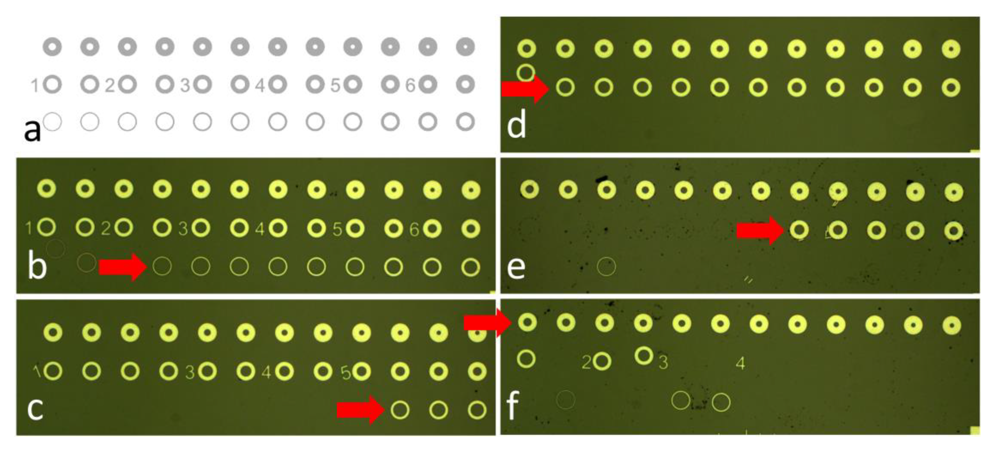
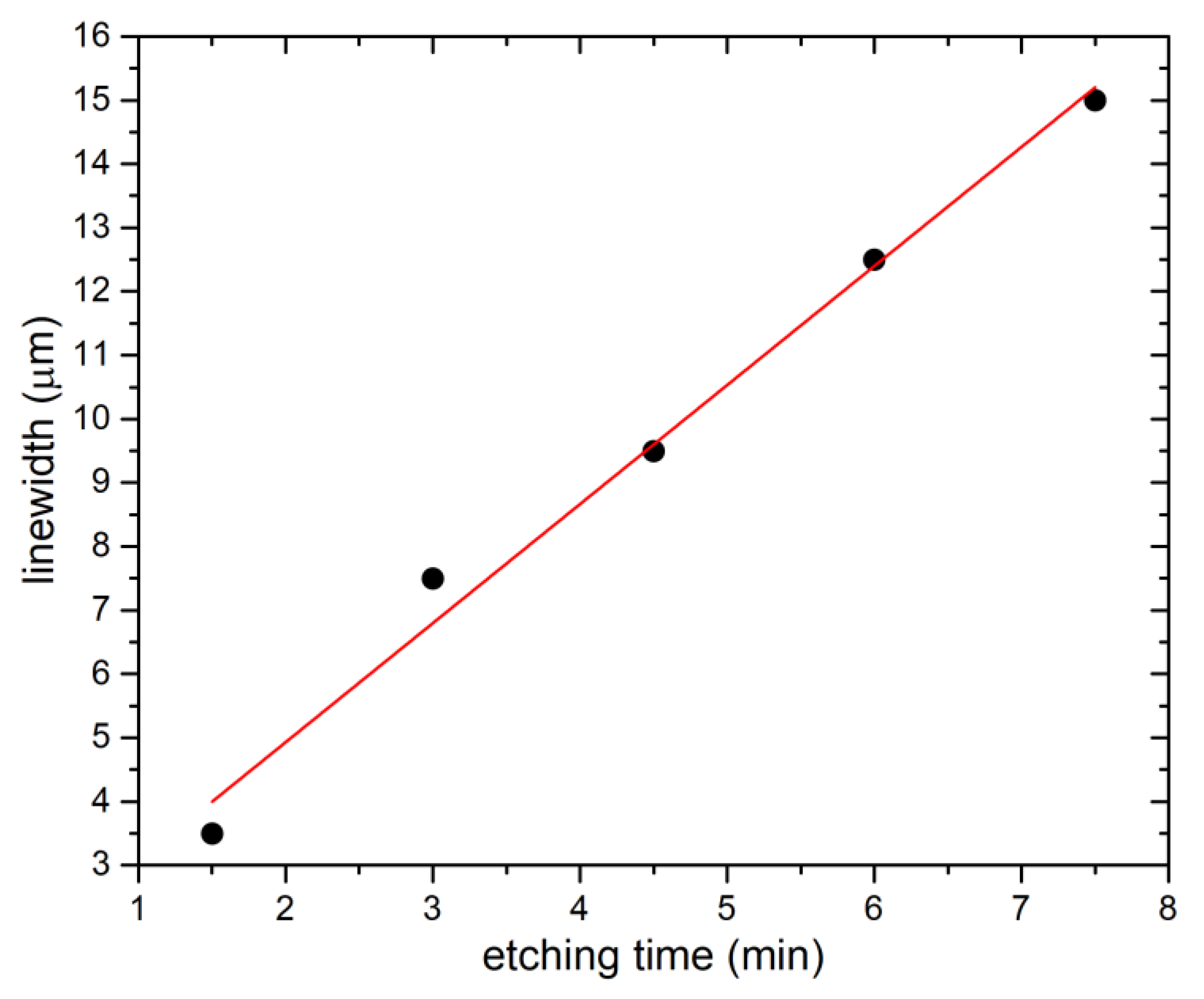
First, we determined the etch rate of SiO2. We observed the etched structures using optical microscope and evaluated torus shapes washed away from the surface, i.e., completely undercut (Figure 1b–f). The last structures not fully undercut with their linewidths (Table 1) were 3.5 µm, 7.5 µm, 9.5 µm, 12.5 µm, and 15.0 µm for etching durations of ≈1.5 min, ≈3.0 min, ≈4.5 min, ≈6.0 min, and ≈7.5 min, respectively. The half of a linewidth of last surviving torus was plotted as a function of time (Figure 2), with its slope defining the SiO2 etch rate as (0.93 ± 0.05) µm∙min−1 (mean ± fitting error), which is ≈14× faster than BOE with 6:1 ratio of 48% HF and 40% NH4F [29].
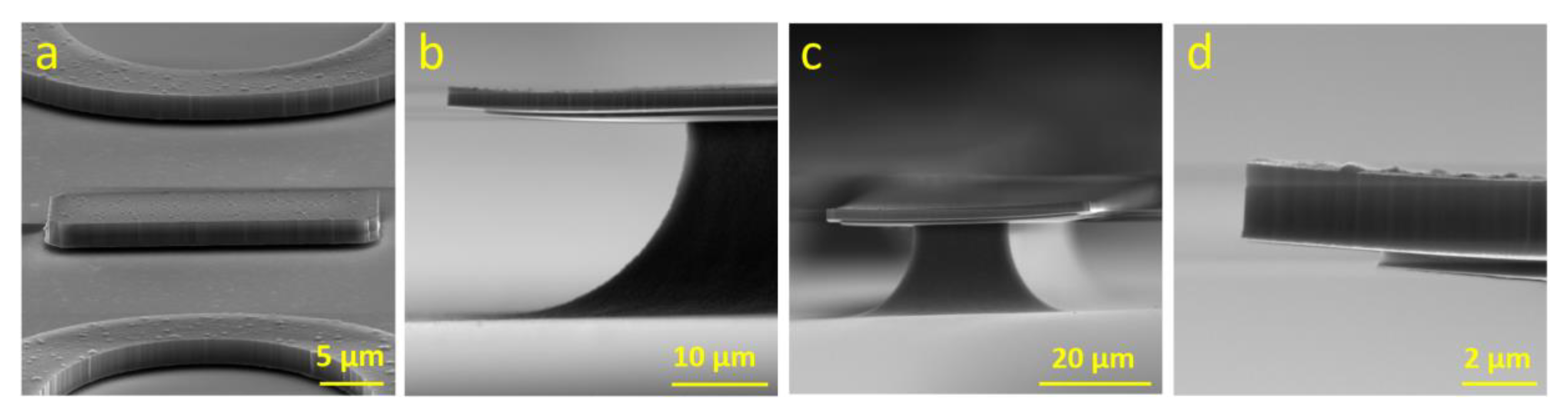
Next, we etched samples in XeF2 vapor and set pressure and time to 0.33 Pa and 225 s, respectively, divided into 5 cycles to increase contrast between SiO2 and Al, and then checked them using scanning electron microscopy (SEM). SEM images show that the both Al and SiO2 layers were not mechanically damaged (Figure 3).
We measured the Al thickness by stylus profiler at the structures used for SiO2 etch rate testing and found that it was (1887 ± 46) nm (mean ± standard deviation from 3 measurements) of whole Al/SiO2 sandwich. These results show that the etching time had no influence on the sandwich thickness.
We measured Al sheet resistance (R□), before and after dipping it into SiO2 etch solution for ≈9 min. We used a custom-made four-point probe system, set the electric current (I) on the outer probes to the range from 10 mA to 60 mA, while monitoring the voltage (V) measured between the inner probes (Figure 4). Then we performed linear curve fitting determining the slope V∙I−1 and calculated the R□ value using the following equation:
We calculated the R□ value of the Al layer from the geometry factor constant and the slope (Figure 4) [30], before and after SiO2 etching for ≈9 min, as (27.8 ± 1.0) mΩ∙□−1 and (29.9 ± 1.2) mΩ∙□−1, respectively (both mean ± fitting errors from five measurements). The small increase in R□ values before and after SiO2 etching was probably caused by measuring on different area of substrate which can be influenced by Al thickness inhomogeneity and impurities on surface as the results from stylus profiler shown that the etch time had no influence on the Al thickness.
Here we summarize advantages and disadvantages of both, dry and wet etching systems. Dry etching is a convenient, user friendly and safe technique using a load lock system practically eliminating an option of an operator to get into contact with the HF gas. Also, there is no need for critical dry release of the structure, as there is no liquid involved in the process. The disadvantage is often prohibited cost of the system as well as its slow etch rate of ≈15 nm∙min−1.
The wet etch proposed in this contribution has a high etch rate of (0.93 ± 0.05) µm∙min−1 (mean ± fitting error), as well as requiring practically no special equipment besides a fume hood, PTFE beaker and personal protective equipment. The disadvantage is requirement of critical dry release or similar method to prevent the MEMS structures to collapse. Also, this etching technique should only be performed by skilled personnel, as they will be dealing with hazardous chemicals. Disposing the etch solution should be done in an appropriate manner using conventional HF types of waste.
5. Conclusions
We proposed and verified the wet SiO2 etching method with excellent selectivity towards Al, practically leaving the Al layer intact. HF solution in the absence of H2O does not etch Al; thus, we used 48% HF in combination with oleum to etch SiO2 by HF, with concurrent removal of H2O, product of SiO2 etching by hygroscopic oleum. We tested this idea by etching thermally grown SiO2, achieving a very high etch rate of (0.93 ± 0.05) µm∙min−1 (mean ± fitting error from three measurements), ≈14× faster in comparison with a typical 6:1 BOE etch rate ≈70 nm∙min−1. During this process, the SiO2 and the Al layer present at the tested chip remained intact, as the sheet resistance before and after exposure to the solution stayed almost the same. The presented method is a simple alternative to anhydrous gas HF etching of SiO2, sacrificial etching, with the Al layer presented on the substrate conducted by complex gas systems.
Author Contributions
P.N. conceived of the idea of this work, designed and performed the experiments. I.G., J.B., J.P., and P.N. performed the experiments. All authors have read and agreed to the published version of the manuscript.
Funding
We acknowledge the support of Grant Agency of the Czech Republic under the contract GJ18-06498Y and support of the Ministry of Education, Youth and Sports of the Czech Republic under the project OP VVV CEITEC Nano+ (CZ.02.1.01/0.0/0.0/16_013/0001728). CzechNanoLab project LM2018110 funded by MEYS CR is gratefully acknowledged for the financial support of the measurements/sample fabrication at CEITEC Nano Research Infrastructure. The SIX Center of BUT was used to conduct the experiments.
Conflicts of Interest
The authors declare no conflict of interests.
References
- Radamson, H.H.; He, X.; Zhang, Q.; Liu, J.; Cui, H.; Xiang, J.; Kong, Z.; Xiong, W.; Li, J.; Gao, J.; et al. Miniaturization of Cmos. Micromachines 2019, 10, 293. [Google Scholar] [CrossRef] [PubMed] [Green Version]
- Janssen, G.C.; Abdalla, M.M.; Van Keulen, F.; Pujada, B.R.; Van Venrooy, B. Celebrating the 100th Anniversary of the Stoney Equation for Film Stress: Developments from Polycrystalline Steel Strips to Single Crystal Silicon Wafers. Thin Solid Film. 2009, 517, 1858–1867. [Google Scholar] [CrossRef]
- Gablech, I.; Klempa, J.; Pekárek, J.; Vyroubal, P.; Hrabina, J.; Holá, M.; Kunz, J.; Brodský, J.; Neužil, P. Simple and Efficient Aln-Based Piezoelectric Energy Harvesters. Micromachines 2020, 11, 143. [Google Scholar] [CrossRef] [PubMed] [Green Version]
- Petersen, K.E. Silicon as a Mechanical Material. Proc. IEEE 1982, 70, 420–457. [Google Scholar] [CrossRef]
- Dutta, S.; Imran, M.; Kumar, P.; Pal, R.; Datta, P.; Chatterjee, R. Comparison of Etch Characteristics of Koh, Tmah and Edp for Bulk Micromachining of Silicon (110). Microsyst. Technol. 2011, 17, 1621. [Google Scholar] [CrossRef]
- Hamzah, A.A.; Aziz, N.A.; Majlis, B.Y.; Yunas, J.; Dee, C.F.; Bais, B. Optimization of Hna Etching Parameters to Produce High Aspect Ratio Solid Silicon Microneedles. J. Micromech. Microeng. 2012, 22, 095017. [Google Scholar] [CrossRef]
- Rangelow, I.W.; Löschner, H. Reactive Ion Etching for Microelectrical Mechanical System Fabrication. J. Vac. Sci. Technol. B Microelectron. Nanometer Struct. Process. Meas. Phenom. 1995, 13, 2394–2399. [Google Scholar] [CrossRef]
- Laerme, F.; Schilp, A.; Funk, K.; Offenberg, M. Bosch Deep Silicon Etching: Improving Uniformity and Etch Rate for Advanced Mems Applications. In Proceedings of the Paper presented at the Technical Digest. IEEE International MEMS 99 Conference. Twelfth IEEE International Conference on Micro Electro Mechanical Systems (Cat. No. 99CH36291), Orlando, FL, USA, 21–21 January 1999. [Google Scholar]
- Eisele, K.M. Sf 6, a Preferable Etchant for Plasma Etching Silicon. J. Electrochem. Soc. 1981, 128, 123–126. [Google Scholar] [CrossRef]
- Winters, H.F.; Coburn, J.W. The Etching of Silicon with Xef2 Vapor. Appl. Phys. Lett. 1979, 34, 70–73. [Google Scholar] [CrossRef]
- Svatoš, V.; Gablech, I.; Ilic, B.R.; Pekárek, J.; Neužil, P. In Situ Observation of Carbon Nanotube Layer Growth on Microbolometers with Substrates at Ambient Temperature. J. Appl. Phys. 2018, 123, 114503. [Google Scholar] [CrossRef]
- Kovacs, G.T.A.; Maluf, N.I.; Petersen, K.E. Bulk Micromachining of Silicon. Proc. IEEE 1998, 86, 1536–1551. [Google Scholar] [CrossRef] [Green Version]
- Guan, D.; Bruccoleri, A.R.; Heilmann, R.K.; Schattenburg, M.L. Stress Control of Plasma Enhanced Chemical Vapor Deposited Silicon Oxide Film from Tetraethoxysilane. J. Micromech. Microeng. 2013, 24, 027001. [Google Scholar] [CrossRef]
- Judy, J. Microelectromechanical Systems (Mems): Fabrication, Design and Applications. Smart Mater. Struct. 2001, 10, 1115–1134. [Google Scholar] [CrossRef] [Green Version]
- Tarraf, A.; Daleiden, J.; Irmer, S.; Prasai, D.; Hillmer, H. Stress Investigation of Pecvd Dielectric Layers for Advanced Optical Mems. J. Micromech. Microeng 2003, 14, 317–323. [Google Scholar] [CrossRef]
- Hornbeck, L.J. Current Status of the Digital Micromirror Device (Dmd) for Projection Television Applications. In Proceedings of the Paper presented at the IEEE International Electron Devices Meeting, Washington, DC, USA, 5–8 December 1993. [Google Scholar]
- Tea, N.H.; Milanovic, V.; Zincke, C.A.; Suehle, J.S.; Gaitan, M.; Zaghloul, M.E.; Geist, J. Hybrid Postprocessing Etching for Cmos-Compatible Mems. J. Microelectromech. Syst. 1997, 6, 363–372. [Google Scholar] [CrossRef] [Green Version]
- Domanský, K.; Petelenz, D.; Janata, J. Effect of Thermal Treatment of Passivation Integrity of Chemical Vapor Deposition Silicon Nitride. Appl. Phys. Lett. 1992, 60, 2074–2076. [Google Scholar] [CrossRef]
- Jang, W.I.; Choi, C.A.; Lee, M.L.; Jun, C.H.; Kim, Y.T. Fabrication of Mems Devices by Using Anhydrous Hf Gas-Phase Etching with Alcoholic Vapor. J. Micromech. Microeng 2002, 12, 297. [Google Scholar] [CrossRef]
- Witvrouw, A.; Bois, B.D.; de Moor, P.; Verbist, A.; van Hoof, C.A.; Bender, H.; Baert, C. Comparison between Wet Hf Etching and Vapor Hf Etching for Sacrificial Oxide Removal. In Proceedings of the Paper presented at the Micromachining and Microfabrication Process Technology VI, Santa Clara, CA, USA, 25 August 2000. [Google Scholar]
- Gennissen, P.T.J.; French, P.J. Sacrificial Oxide Etching Compatible with Aluminum Metallization. In Proceedings of the International Solid State Sensors and Actuators Conference (Transducers ’97), Chicago, IL, USA, 19–19 June 1997; Volume 1, pp. 225–228. [Google Scholar]
- Clews, P.J.; Mani, S.S. Selective Etchant for Oxide Sacrificial Material in Semiconductor Device Fabrication. U.S. Patent 6,893,578, 17 May 2005. [Google Scholar]
- Amini, B.V.; Abdolvand, R.; Ayazi, F. A 4.5-Mw Closed-Loop $\Delta\Sigma $ Micro-Gravity Cmos Soi Accelerometer. IEEE J. Solid State Circuits 2006, 41, 2983–2991. [Google Scholar] [CrossRef]
- Kuehnel, W.; Sherman, S. A Surface Micromachined Silicon Accelerometer with on-Chip Detection Circuitry. Sens. Actuators A Phys. 1994, 45, 7–16. [Google Scholar] [CrossRef]
- Syllaios, A.J.; Schimert, T.R.; Gooch, R.W.; McCardel, W.L.; Ritchey, B.A.; Tregilgas, J.H. Amorphous Silicon Microbolometer Technology. MRS Online Proc. Libr. Arch. 2000, 609, A14.4. [Google Scholar] [CrossRef]
- Sedky, S.; Fiorini, P.; Baert, K.; Hermans, L.; Mertens, R. Characterization and Optimization of Infrared Poly Sige Bolometers. IEEE Trans. Electron Devices 1999, 46, 675–682. [Google Scholar] [CrossRef]
- Akhavan, J. The Chemistry of Explosives; Royal Society of Chemistry: London, UK, 2011. [Google Scholar]
- Balram, K.C.; Westly, D.A.; Davanco, M.; Grutter, K.E.; Li, Q.; Michels, T.; Ray, C.H.; Yu, L.Y.; Kasica, R.J.; Wallin, C.B.; et al. The Nanolithography Toolbox. J. Res. Natl. Inst. Stand. Technol. 2016, 121, 464–475. [Google Scholar] [CrossRef]
- Walker, P.; Tarn, W.H. Crc Handbook of Metal Etchants; CRC press: Boca raton, FL, USA, 1990. [Google Scholar]
- Miccoli, I.; Edler, F.; Pfnür, H.; Tegenkamp, C. The 100th Anniversary of the Four-Point Probe Technique: The Role of Probe Geometries in Isotropic and Anisotropic Systems. J. Phys. Condens. Matter 2015, 27, 223201. [Google Scholar] [CrossRef] [PubMed]
Figure 1.
Test structure to determine the SiO2 etch via lateral under etching. (a) Structure layout containing structures with identical outer diameter and different width starting from 2 µm and ending with 20 µm with step of 0.5 µm. Photographs of structures after SiO2 etching for: (b) ≈1.5 min, (c) ≈3.0 min, (d) ≈4.5 min, (e) ≈6.0 min and (f) ≈7.5 min. The red arrow points at the torus shape with the smallest linewidth not fully undercut.

Figure 2.
SiO2 etching as function of time. The curve was obtained as linear approximation for six etched samples for different time in range from ≈1.5 min to ≈7.5 min with an interval of ≈1.5 min.
Figure 2.
SiO2 etching as function of time. The curve was obtained as linear approximation for six etched samples for different time in range from ≈1.5 min to ≈7.5 min with an interval of ≈1.5 min.

Figure 3.
SiO2 etched with HF/oleum, showing the undercutting with Al layer intact: (a) Structures undercut by SiO2 etch solution leaving intact Al. (b) The same etching of SiO2 followed by partial Si removal by XeF2 vapor to enhance visibility of SiO2 etch boundary. (c) Different angle and magnification show whole structure (d) and corner detail.

Figure 4.
Graphs showing the value of V as a function of interrogating I from the four-point probe system at Al layer before (a) and after (b) dipping in SiO2 etch solution. The fitted slope V∙I−1 with an assumption of intercept of 0 V changed by ≈7.5%.
Figure 4.
Graphs showing the value of V as a function of interrogating I from the four-point probe system at Al layer before (a) and after (b) dipping in SiO2 etch solution. The fitted slope V∙I−1 with an assumption of intercept of 0 V changed by ≈7.5%.


Table 1.
Line width of the layout shown in Figure 1a having three rows and 12 columns. Please note that there was a mistake on the layout, and thus the linewidths with size of 6.5 µm and 7.0 µm are missing.
Table 1.
Line width of the layout shown in Figure 1a having three rows and 12 columns. Please note that there was a mistake on the layout, and thus the linewidths with size of 6.5 µm and 7.0 µm are missing.
| Column/Row | 1 | 2 | 3 | 4 | 5 | 6 | 7 | 8 | 9 | 10 | 11 | 12 |
|---|---|---|---|---|---|---|---|---|---|---|---|---|
| 1 | 15.0 | 15.5 | 16.0 | 16.5 | 17.0 | 17.5 | 18.0 | 18.5 | 19.0 | 19.5 | 20.0 | 20.0 |
| 2 | 9.0 | 9.5 | 10.0 | 10.5 | 11.0 | 11.5 | 12.0 | 12.5 | 13.0 | 13.5 | 14.0 | 14.5 |
| 3 | 2.0 | 2.5 | 3.0 | 3.5 | 4.0 | 4.5 | 5.0 | 5.5 | 6.0 | 7.5 | 8.0 | 8.5 |
© 2020 by the authors. Licensee MDPI, Basel, Switzerland. This article is an open access article distributed under the terms and conditions of the Creative Commons Attribution (CC BY) license (http://creativecommons.org/licenses/by/4.0/).
Share and Cite
MDPI and ACS Style
Gablech, I.; Brodský, J.; Pekárek, J.; Neužil, P. Infinite Selectivity of Wet SiO2 Etching in Respect to Al. Micromachines 2020, 11, 365. https://doi.org/10.3390/mi11040365
AMA Style
Gablech I, Brodský J, Pekárek J, Neužil P. Infinite Selectivity of Wet SiO2 Etching in Respect to Al. Micromachines. 2020; 11(4):365. https://doi.org/10.3390/mi11040365
Chicago/Turabian StyleGablech, Imrich, Jan Brodský, Jan Pekárek, and Pavel Neužil. 2020. "Infinite Selectivity of Wet SiO2 Etching in Respect to Al" Micromachines 11, no. 4: 365. https://doi.org/10.3390/mi11040365
Note that from the first issue of 2016, this journal uses article numbers instead of page numbers. See further details here.