
Abstract
We present a novel technique to perform contactless and mask-free patterned plasma enhanced chemical vapour deposition and etching. When a powered electrode with narrow slits is placed very close to the substrate, plasma is selectively ignited within the slits due to the hollow cathode effect, and so deposition or etching occurs only within an area smaller than the size of the slit. This technique is demonstrated through the deposition of hydrogenated amorphous silicon using a gas mixture of hydrogen, argon and silane. Slits as small as 1 mm generate a plasma, and for this width, the lines deposited are about 750 μm wide, homogenous over their length (60 mm), and are deposited at a rate of 50 nm min−1. The phenomenon is studied using 2D Particle In Cell (PIC) modelling with a simplified argon chemistry. The electron localization observed in the PIC modelling provides an explanation of why the deposition is narrower than the slit.
Export citation and abstract BibTeX RIS

Original content from this work may be used under the terms of the Creative Commons Attribution 3.0 licence. Any further distribution of this work must maintain attribution to the author(s) and the title of the work, journal citation and DOI.
Introduction
A well-known advantage of low-temperature plasma processing is its ability to provide uniform surface treatments over large areas. This uniformity finds advantageous applications in fields such as etching and deposition on wafers for the semiconductor industry (for wafers with diameters up to 450 mm) and for thin film deposition for flat panel displays and solar cells (substrates with areas up to almost 10 m2).
To enable this advantage in practice, great engineering efforts have gone into understanding and mitigating sources of non-uniformity. These sources of non-uniformity may originate from electromagnetic standing waves coupling with plasma skin effects [1], gas depletion [2], powder formation [3, 4], hollow cathode effects due to chamber design, but also due to more simple technological considerations such as thermal non-uniformities, and gas flow distribution.
Once the desired uniformity of a plasma process is achieved, any localization of the etching or deposition process is then achieved by a masking step, either lithographic (wherein the mask is formed on the substrate, allowing one to achieve feature sizes in the tens of nanometres), through a shadow mask for lower resolution patterning, or through laser ablation. For less stringent patterning requirements, new approaches using microprinting techniques have emerged. Such techniques allow a simple and low cost manufacturing process. For example, using a localized plasma to perform surface activation, one can achieve patterning through area-selective deposition, (i.e. μ-plasma printing) [5].
One such useful material to deposit and pattern is hydrogenated amorphous silicon (a-Si:H). This material has been widely used in the flat panel display and photovoltaics industries. Due to its excellent passivation of crystalline silicon (c-Si) surfaces, it is the key enabling technology for heterojunction silicon solar cells. One very high efficiency architecture for a photovoltaic cell combines the best design for a PV cell (interdigitated back contacts to allow maximum light penetration) with the best junction passivation technology (plasma enhanced chemical vapour deposition, PECVD layers of a-Si:H) [6, 7]. In such architectures, the interdigitated doped areas are either patterned by lithography or use a shadow masking approach [8].
In this work, we demonstrate a technique to deposit a patterned a-Si:H semiconductor film over large areas by PECVD. The described technique localizes the plasma formation to limited volumes through the use of a patterned electrode, and achieves maskless lithography with a resolution on the order of hundreds of micrometres, without ever contacting the surface.
Experimental details
The experiments presented herein were performed in a single chamber PECVD reactor with a grounded substrate holder, and a four-inch diameter radio-frequency (RF) powered electrode designed to implement the desired patterned deposition. Both substrate holder and electrode were at room temperature, and no active cooling was performed. The patterned RF electrodes used for these experiments were powered using a 13.56 MHz voltage source. Both the RF power and the peak-to-peak voltage at the feedthrough were recorded. During the experiments, the electrodes were not actively cooled; their temperatures were monitored but never increased by more than 10 °C.
Two different electrode designs were used in these experiments. In both cases, the electrodes were fabricated out of aluminium, and contained a hollow central volume as well as a substrate-facing plate with multiple narrow slits.
The first electrode (electrode A) is presented in figure 1(a). It has a diameter of 84.5 mm, and contains 13 slits that are 60 mm long and have widths varying from 0.5 to 2.5 mm with spacing varying from 0.5 to 3.5 mm. The top plate was 3 mm thick and the profile of the slits is rectangular, as they were formed through laser cutting. Figure 1(b) shows an image of an argon plasma discharge in the slits, as viewed through a transparent substrate with a conductive coating and a viewing port in the substrate holder.

Figure 1. (a) Photograph of patterned Electrode A composed of 13 slits with different widths and spacings. (b) Photo taken through transparent substrate shows plasma ignited within the slits of the electrode.
Download figure:
Standard image High-resolution imageThe second electrode (Electrode B), as depicted in figure 2(a) was designed and fabricated with slits that are all 1 mm wide at a 10 mm pitch. The slits are also 60 mm long and, as before, the electrode was hollow to allow gas injection and distribution. The front plate thickness was again 3 mm, and the slits were rectangular in cross-section, as shown in the diagram of figure 2(b).

Figure 2. (a) Photograph of second design, patterned Electrode B, for deposition on 4 inch wafers. The slits are 60 mm long and 1 mm wide. They are spaced 10 mm apart. The top plate has a 84.5 mm diameter and is 3 mm thick. (b) Cross sectional view of electrode cavity, including slits, substrate, and substrate holder.
Download figure:
Standard image High-resolution imageThe patterned layers were characterized by profilometry, Raman scattering, and spectroscopic ellipsometry. A Dektak XT profilometer was used to measure line thickness and to obtain 3D mapping of lines in order to investigate the uniformity of patterned deposition. A UVISEL 2 spectroscopic ellipsometer from Horiba was used to cross-check layer thickness and to characterize a-Si:H quality.
Results
Electrode A was used for the first set of experiments. Corning glass substrates (1.1 mm thick) were used, and particular attention was paid to plasma ignition as a function of slit width. A deposition was performed using a H2/SiH4 flow ratio of 70:10.5, at a pressure of 6 Torr, and nominal RF power of 70 W. These deposition conditions were arrived at through trial and error and were chosen as they resulted in a stable discharge and a lack of the formation of powders. It should be noted that the power value includes the power sent to parasitic plasmas when and if they ignite outside of the slits and so does not have much significance. Substantial care was taken in subsequent designs to minimize the ignitions of these parasitic plasmas. The power of 70 W corresponded to a peak to peak voltage of about 450 V, as measured at the RF feedthrough on the reactor. The deposition was done after placing the RF electrode (with the hollow cathode slits) at a position 0.5 mm from the substrate. The pressure measurements in all of these experiments were acquired outside of the electrode assembly, in the vacuum vessel. To verify that the pressure measured in the vessel corresponded well to that of the discharge area, Computational Fluid Dynamics simulations (ANSYS software) were performed using the exact chamber geometry and gas flow rates. Those simulations confirmed that for a judicious choice of electrode design, the gas distribution was uniform and the pressure drop between the slits and the measurement point was only about 7%.
The results of the deposition can be seen in figure 3. Figure 3(a) shows a photograph of a patterned deposition on the Corning Glass substrate. These films adhered well to the substrate and no stress-based delamination has been observed. It can be noted that deposition only occurred within the 2.5 mm wide slits, indicating that a plasma only ignited within these slits. It is worth noticing that no deposition occurs between the slits, while deposition at a rate of 6 Å s−1 is observed within the slit opening. Furthermore, the patterned deposition reproduces the electrode design independent of the spacing between the slits. Figure 3(b) presents a 3D profilometry mapping for three adjacent slits. Figure 3(c) is a Raman scattering spectrum acquired on these films, showing that they are composed of a-Si:H with no appreciable nanocrystalline component.

Figure 3. (a) Picture of the patterned deposition on Corning glass using Electrode A and the 2.5 mm wide slits. (b) 3D mapping obtained from profilometry measurement on the lines deposited from the 2.5 mm wide slits. (c) Raman scattering spectrum acquired from sample.
Download figure:
Standard image High-resolution imageIn figure 4(a), we present profilometry scans obtained at five different positions. It can be observed that all the lines feature a thickness around 430 nm with a variation of 15 nm from one line to the other. Moreover it does not show significant variation of width along the 60 mm lines. Therefore for 2.5 mm wide slits the deposition is uniform in these process conditions. Figure 4(b) represents the normalized thickness of layers deposited in the same process conditions but for three different deposition times leading to 10, 50 and 500 nm thick layers. It indicates that the cross-section shape is not significantly affected by the layer thickness and that regardless of the film thickness deposited, a 'Gaussian-like' profile is observed.

Figure 4. (a) Profilometry scans performed on patterned deposition layers from 2.5 mm wide slits. (b) Comparison of normalized thickness between patterned lines deposited in the same process conditions but for different deposition times.
Download figure:
Standard image High-resolution imageIn a second set of experiments using Electrode A, particular effort was made to ignite a plasma in the narrower sets of slits. A typical result is present in figure 5(a). Contrary to the deposition in front of the 2.5 mm slits, the patterned deposition in front of the 1.5 mm slits is not well defined and the deposition rate is significantly lower. As well, optical microscopy shows that the line deposited in front of the 1.5 mm slit has a width of 1.2 mm (not shown), and nothing is deposited in front of the 0.5 mm slit. The lines deposited in front of the 2.5 mm slits are still composed of a-Si:H, and adhere well to the surface. The observable non-uniformity is due to thickness variations.

Figure 5. Picture of patterned deposition on Corning Glass using Electrode A. Deposition occurs for both 2.5 and 1.5 mm wide slits. The deposition rate is much higher for the 2.5 mm wide slits, and no deposition is observable for the 0.5 mm wide slits. Of note, the lines deposited below the 1.5 mm silts are 1.2 mm wide.
Download figure:
Standard image High-resolution imageElectrical measurements at the RF feedthrough made during this experiment help explain this result. It was observed that before plasma ignition, increasing power was accompanied by increasing peak-to-peak voltage. However, once a plasma was ignited (in the widest, 2.5 mm slits), further increase in power resulted in little increased voltage. Once a plasma ignites in larger slit, it is difficult to obtain ignition in a narrower slit, as all additional power is dumped into the wider slit as current, rather than as a greater voltage.
Nevertheless, looking at the lines deposited below the 1.5 mm wide slits with optical microscopy, a line width of 1.2 mm is measured. As was observed with the larger 2.5 mm slits (where the linewidth was ∼1.5 mm), the lines are narrower than the slits from which they are deposited.
Finally, it is noted that these first experiments did not determine the lower bound of slit width for which ignition would occur, due to the presence of wider slits. The second design, Electrode B, was imagined to eliminate this problem by using all identically sized slits.
The second design, Electrode B, was fashioned with a set of identically dimensioned slits to avoid the problem of selective slit ignition. The four slits were all 1 mm wide, but still 60 mm in length. For these sets of samples, a gas mixture consisting of H2/Ar/SiH4 at flow rates of 80/8/0.5 sccm was used, and a total process pressure of 9 Torr was maintained. This higher pressure is due to the smaller dimensions involved (1 mm slits), and one can calculate a pressure-distance product of 1 Torr cm, which is a reasonable value for plasma ignition. Furthermore, argon was added to the gas mixture to facilitate plasma ignition and stability. A coupled RF power of 40 W was measured; this included power coupled to parasitic plasmas, but which was reduced in this design. Deposition was performed on a silicon wafer, and a photograph of the results is presented in figure 6(a). The very homogenous deposition along the slit is again observed, as well as parasitic deposition at the edge of the electrode and at the three screw locations. When only 1 mm slits are used, the plasma lights easily within these slits, and the deposition is uniform along their length. Furthermore, despite the very high process pressure and use of Ar, no powders are observed on the substrate after the process.

Figure 6. (a) Picture of patterned deposition using the second electrode with 1 mm slit width. (b) Zooming by optical microscopy in the patterned deposition layer in (a).
Download figure:
Standard image High-resolution imageFigure 6(b) shows an optical microscope image of the deposited a-Si:H layer. The patterned layers obtained from this electrode are again narrower than the slit width. In these process conditions, the line is 0.76 mm wide while the slit is 1 mm wide.
The deposition was further characterized using ellipsometry (using the appropriate optical model for a-Si:H) and profilometry measurements, and comparison between the thicknesses obtained from these two techniques is shown in figure 7(a). As one can see, both characterization techniques converge toward same values with a central thickness of 250 nm, which, for a 5 min deposition time, corresponds to a deposition rate of 50 nm min−1. In figure 7(b), a 3D mapping of the line by profilometry shows an excellent uniformity of the line (±5% in thickness) along 10 mm of its length. Again, the films adhered well to the substrate and no delamination was observed with time. The homogeneity in thickness and width of these lines underlines an important feature of this deposition technique, which is the dependence on the nature of the substrate. As the substrate thickness is a significant, even dominant fraction of the gap (1 or 0.3 mm, versus a gap of 0.5 mm), the ease of lighting a stable and uniform plasma changes with the substrate, as the proportion of electric field dropped in the substrate will change. The c-Si substrate was most beneficial, as it filled the entirety of the electrode surface, was perfectly uniform, and was thinner.

Figure 7. Profilometry scan (left) and 3D mapping of profilometry data (right) acquired along a 10 mm length of the line.
Download figure:
Standard image High-resolution imageDiscussion
The most interesting outcome to be explained from the above results is that the line width of the deposited strips of a-Si:H is consistently smaller than the slit opening. This is an interesting feature from a scientific and technological point of view, as it indicates that micro scale deposition can be expected by optimizing the design and the plasma parameters. Furthermore, the particular configuration of the slits suggests the presence of the hollow cathode discharge effect. Hollow cathode (HC) discharges have been investigated as a method to increase the deposition rate of amorphous silicon and silicon nitride, either in a plasma jet configuration [9–12], or as a set of remote sources in a large area PECVD reactor [13, 14]. The high deposition rates achieved (up to 10 μm min−1) are attributable to the high plasma density [15, 16] and the specific ion and electron energies [17–19] induced by the HC effect. In the experiments listed above, however, the overriding goal was the deposition of a homogenous layer over a large area, i.e. overcoming the localization intrinsic to the HC effect. In our implementation, the controlled localization is a benefit to be exploited, but is still governed by the same physics.
To better understand the origin of this result, plasma simulations have been performed to numerically model the plasma behaviour in an individual HC. In contrast to the experiments, the modelling was performed using only argon, with the goal of capturing some of the basic features of the plasma. The software used herein is an extension of the PHOENIX 1D code, an academic particle-in-cell (PIC) simulation algorithm, which has been previously described in [20, 21]. The code follows typical PIC and Monte Carlo collision (MCC) algorithms [22, 23], but has been extended to simulate a 2D CCP system. The argon plasmas are modelled with electron-neutral cross-sections (elastic, excitation and direct ionization) taken from [24], and ion-neutral cross-sections (isotropic and backward scattering) from [25]. The density of the neutral gas is assumed to be spatially constant with a temperature of 300 K. The gas temperature was never measured within the discharge region in the experiments, and so gas heating due to the higher power density may locally reduce the gas density in the slits. Electrons are reflected from the boundaries with a probability of 0.2, and the secondary electron emission coefficient due to ion bombardment is set to 0.1. The simulation used 400 grid points, with 3000 time steps per RF period T = 1/f, where f is the RF frequency (13.56 MHz). The peak-to-peak RF voltage used was 450 V. This value is similar to the voltages measured at the RF feedthrough for the experimental work. Simulations are run to steady-state with about 100 000 super-particles, after which the relevant diagnostics are averaged over many RF periods.
The modelling was performed for a system consisting of an infinite single slit in the RF electrode (figure 8(a)), and for two different dimensions of slit: the first with a 2.0 mm aperture and a 1.5 mm depth (figure 8(b)), and the second with a 1.5 mm aperture and a 3.5 mm depth (as shown in figure 8(c)). In both configurations, the inter-electrode distance away from the hollow cathode is 0.5 mm, and periodic boundary conditions are set at these simulation space edges.
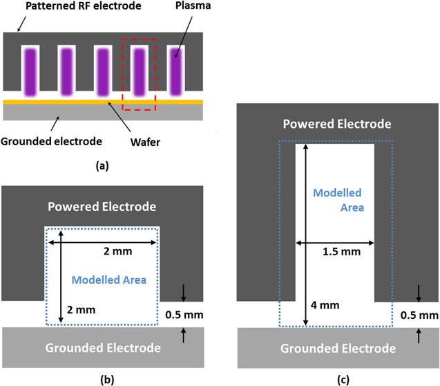
Figure 8. Schematic of RF patterned electrode, (b) first configuration of modelled area (2 mm × 2 mm), and (b) second configuration (1.5 mm × 4 mm).
Download figure:
Standard image High-resolution imageFor the first configuration, (2 mm × 2 mm), the results of the PIC simulation are presented in figure 9, showing the spatial distribution of the electron density and the electrical potential at four different times in the RF cycle. The four rows shown are at the peak of the RF voltage (330 V, figures 9(a) and (e)), the first zero crossing (figures 9(b) and (f))), the RF voltage minimum (−120 V, figures 9(c) and (g)), and the second zero crossing (figures 9(d) and (h)). One can note that the DC self-bias voltage in this simulation is positive, which is logical, as the surface area of the powered electrode is larger than that of the grounded one. As well, the electron density profile at all four points of the cycle is confined to the middle of the discharge region. Interestingly, this is even true at the minimum voltage (figure 9(c)). Although below the dashed line there is no lateral confinement by the electrode, the 'cloud' of electrons still remains localized within the projected zone below the hollow cathode.

Figure 9. PIC simulation results showing instantaneous electron density (a)–(d) and potential distributions (e)–(h) within hollow cathode region for four points in the RF cycle: peak of RF voltage (top, (a)/(e)), first zero-crossing (middle top, (b)/(f)), minimum RF voltage (middle bottom, (c)/(g)) and second zero-crossing (bottom, (d)/(h)).
Download figure:
Standard image High-resolution imageIn figures 10 and 11, simulation results are presented for the second configuration (1.5 mm × 4.0 mm). Figure 10 again shows the spatial distribution of the electrical potential and the electron density at the minimum in the voltage waveform. Again, one can observe the localization of the electrons to an area much narrower that the width of the gap. In figure 11, the instantaneous profile of the argon ion density and flux are shown (for the Ar+ flux, note that the positive values indicate flux towards the substrate). The profiles are shown at the same point in the RF cycle as for figure 10, the minimum in the RF potential applied to the top electrode. One can note that the ion flux towards the substrate is also localized to an area smaller than the size of the hollow cathode. As well, the profiles of ion flux does change appreciably within an RF cycle due to the very high voltages and the very small distances involved.

Figure 10. Results of PIC simulation, displaying profiles of instantaneous (a) electron density, and (b) electrical potential in the hollow cathode, at the moment of the minimum in the RF potential (applied to the top electrode).
Download figure:
Standard image High-resolution image
Figure 11. Results of PIC simulation, displaying profiles of instantaneous (a) argon ion density and (b) argon ion flux in the hollow cathode. Shown at same moment as figure 10.
Download figure:
Standard image High-resolution imageThe instantaneous Ar+ flux at the minimum of the RF cycle shows a profile that is the convolution of both the ion density and the electric field. One can observe a particular shape in this profile, consisting of a central lobe coinciding with the greater ion density, on top of a broader profile that extends across almost the entirety of the gap.
To compare these simulations with experiments, the ion flux at the substrate is averaged over an RF cycle, and is presented in figure 12(a)). In this profile, one can note the broad 'top-hat' profile originating from ions generated throughout the cycle and originating from deeper into the hollow cathode, as well as a narrower peak from those generated very close to the surface by the electron 'cloud' approaching it during the voltage minimum. To compare to this, in figure 12(b)) we also present a profilometry scan for crystalline silicon wafer etched using a patterned electrode with the same design as the above simulation, and for an Ar + H2 plasma. This etching process used process conditions as described above, but without the silane (6 Torr, 80 sccm of H2, 8 sccm of Ar, 70 W, room temperature). As the crystalline wafer will only be etched by H radicals once the surface has been amorphized by an ion, the depth of etching gives a representative record of the integrated ion flux. The similarity between the two curves (consisting of both a broad 'top-hat' as well as a narrower peak) supports the accuracy of the PIC simulations. In fact, looking closely at figure 4(b), a less obvious version of this 'lobed' pattern can be detected, showing that even for complex deposition chemistries, the physics of the plasma in the slit retains the characteristics revealed by the PIC simulations.

Figure 12. (a) Result of PIC simulation of the cycle-averaged ion flux at the substrate surface in argon plasma. (b) Profilometry scan of a crystalline silicon wafer etched by an argon/hydrogen plasma.
Download figure:
Standard image High-resolution image
Conclusion
A new technique has been demonstrated to perform mask-free patterned deposition and etching using a plasma enhanced process. It is advantageous as it allows the lithographic function to be performed (i) directly, including for semiconductor layers that can be deposited using PECVD, (ii) in a contactless fashion, as the technique does not require a mask to be in contact with the substrate, (iii) at high rates without depositing powder, and (iv) in a reactor chamber that can be also used to deposit homogenous, blanket layers simply by backing the electrode away from the surface and changing the process conditions (notably pressure). The use of an RF electrode with narrow slits allows the plasma to ignite only within the slits, and isolates the deposition/growth to an area narrower than the slit width. For the pressure ranges explored, wider slits are easier to light than narrow ones, so an identical set of slits is necessary to achieve ignition within (and growth below) all of the slits. The resolution and types of material that can be deposited make this technique suitable for applications such as interdigitated or point contacts for photovoltaics or photodetection.
Acknowledgments
The authors acknowledge the financial support of Total and the ANR through the PISTOL Industrial Chair Project (ANR-17-CHIN-0002-01). The authors would also like to thank T Lafleur for permitting the use of his PIC code and providing initial training support for BB.