
Abstract
We propose a method to induce deterministic motion of a magnetic domain wall in a nanowire by inducing short strain pulses uniformly along the nanowire. Via inverse magnetostriction, a strain pulse causes the magnetic anisotropy to vary uniformly on a timescale comparable to the magnetisation dynamics. The resultant torque on the magnetic moments within the domain wall cause it to move along the nanowire. Using numerical calculations we analyse in detail the dependence of the domain wall's motion on the material's parameters and on the anisotropy pulse profile, and we consider the specific case of the anisotropy induced by voltage pulses applied to a hybrid piezoelectric/ferromagnet device. The method will be applicable to a range of magnetic textures including skyrmions, solitons, and domain walls in antiferromagnets, and is prospective for applications in a range of areas including ultra-energy efficient information storage and processing, communications technologies, position encoding and biomedical science.
Export citation and abstract BibTeX RIS

Original content from this work may be used under the terms of the Creative Commons Attribution 4.0 licence. Any further distribution of this work must maintain attribution to the author(s) and the title of the work, journal citation and DOI.
A magnetic domain wall separates regions of a magnetic material in which the magnetisation lies along different directions. The ability to control magnetic domain walls is desirable for a range of applications including information storage [1–3] and processing [4, 5], position sensing [6] and in biomedical science [7]. For decades the controlled motion of magnetic domain walls has been possible only by the application of external magnetic fields [8–10] or by the transfer of spin angular momentum from charge carriers to the local magnetic moments [11–16] which can be achieved by driving electrical current through the magnetic specimen. More recently it has been demonstrated that magnetic domain walls can be moved using magnons [17], photons [18] and temperature gradients [19]. There are several proposals to implement magnetic domain walls in magnetic data storage [1–3] and concepts for performing logical processing operations [4, 5] in which information is encoded as the presence or position of a domain wall along a quasi-1D nanowire. The high energy cost associated with generating magnetic fields or passing electrical currents through resistive nanowires, and the difficulty in targeting individual magnetic structures, pose significant practical problems for the implementation of such concepts.
It has been recognised that methods to control magnetic anisotropy by electric field gating [20–22], or by voltage-induced mechanical strain [23–25] offer an energy efficient and practical route to controlling the magnetisation direction, but it has not been clear how such methods can be implemented to move domain walls deterministically and efficiently. In the case of a nanowire, where the magnetic anisotropy is uniform along the length of the wire, there is no energetically favourable position to situate the domain wall. It has been proposed to modulate the magnetic anisotropy along the wire and to carry the domain walls in time varying magnetic anisotropy energy minima. However, such methods require the fabrication of multiple piezoelectric elements along the wire [26] or the generation of complex super-positions of surface acoustic waves [27]. Here we show that by varying a spatially uniform magnetic anisotropy on timescales comparable to the magnetisation precession frequency a torque is induced on the magnetic domain walls which leads to deterministic displacement. Unlike other methods for moving domain walls, the domain wall velocity is not limited by the Walker breakdown in our case [28–30]. Furthermore, the uniform anisotropy pulse can act on multiple domain walls at the same time, creating the same displacement for a sequence of domain walls without the need for complicated electrode fabrication and pulse sequences [26], making the method highly attractive for implementation in information storage concepts, such as the Racetrack memory [2].
We consider the particular case of a magnetic domain wall formed in a nanowire with dominant perpendicular magnetic anisotropy. As depicted in figure 1(a) the magnetic moment orientation rotates across the domain wall, which separates regions where the magnetisation points up or down. The azimuthal angle of the magnetisation with respect to the wire axis at the centre of the domain wall,  , is determined by the material parameters and the wire width. In the cases where
  (or
(or  ) or
) or  the wall can be described as Néel or Bloch type respectively. Figure 1(b) shows a schematic device design that would allow an additional uniform magnetic anisotropy energy,
  , to be induced uniformly in the plane of the magnetic wire by applying a voltage to a piezoelectric mesa upon which the wire is fabricated. The uniaxial mechanical strain created by the piezoelectric induces a uniaxial magnetic anisotropy energy in the plane of the magnetic wire via magnetoelastic coupling. The induced magnetic anisotropy energy will act on the magnetic moments throughout the wire like an effective magnetic field,
  , where E is the contribution to the magnetic free energy due to the strain-induced anisotropy and M is the magnetisation vector. HK will lie along the axis of the induced anisotropy in the direction that minimises the angle between HK and M. This uniaxial effective field will induce a torque on the magnetisation of the form
  , where
  is the gyromagnetic ratio. The direction of the torque will depend on the direction of the local magnetic moment with respect to HK, and therefore depends upon the position of the local moment along the wire, as shown for example in figure 1(a). In the regions of uniform magnetisation, away from the domain wall, the torque will be less effective at rotating the magnetic moments because the strong perpendicular anisotropy and the exchange interaction between neighbouring moments add to stabilise the direction of the magnetisation. Within the domain wall there is an energy cost associated with the canting of magnetic moments away from the perpendicular easy axis and from neighbouring moments. Here, the effective magnetic field induced by the additional in-plane magnetic anisotropy can more effectively rotate the magnetisation vector. In the situation depicted in figure 1(a), this results in a net motion of the domain wall along the wire in the direction shown by the orange arrow. The effect is analogous to the motion of a magnetic domain wall induced by an external magnetic field pulse reported in [31].
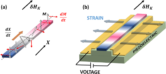
Figure 1. Representation of a magnetic domain wall and a device for displacing a sequence of domain walls using a voltage pulse. (a) A magnetic domain wall formed in a nanowire with perpendicular magnetic anisotropy, and (b) a piezoelectric/ferromagnet device. A voltage pulse applied to electrodes fabricated on a piezoelectric mesa creates a strain pulse in the ferromagnetic wire which induces motion of a sequence of domain walls.
Download figure:
Standard image High-resolution imageThe 1D model
To explore the motion of the domain wall and its dependence on experimental parameters we simulate the motion of the magnetic domain wall using the rigid 1D model, which has been shown to provide a good qualitative description of domain wall motion along nanowire strips with perpendicular magnetic anisotropy [32]. Equations (1) and (2) describe the domain wall dynamics in terms of the position  and the azimuthal angle
  ,
,
where  is the Gilbert damping parameter. The width of the wall,
  is determined by the perpendicular magnetic anisotropy energy,
  and the exchange stiffness parameter, A. Following [33] we model the preference for forming a Bloch or Néel type wall by an effective field HK in the plane of the wire. Positive (negative) HK favours the formation of a Bloch (Néel) wall. HK is determined, among other factors, by the parameters of the magnetic material and the width of the nanowire [13]. We model the effects of a time varying induced in-plane magnetic anisotropy, KU as a variation of the sign and magnitude of HK by the addition of a term
  , where the field is ramped up to the value δHK over time δt from the beginning of the simulation.
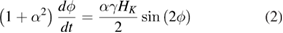
Equations (1) and (2) were solved numerically by implementing a fourth order Runge–Kutta method with a time step of 1ps. Figures 2(a) and (b) confirm the main result of this article: that an induced uniaxial anisotropy induces motion of the domain wall along the x-axis. Positive (negative) KU transforms the domain wall from Néel (Bloch) to Bloch (Néel) type and induces domain wall motion in the negative (positive) direction. The rate at which the domain wall is displaced depends on several factors including the rate at which the anisotropy is induced, the damping coefficient and the domain wall width. Figures 2(c) and (d) demonstrate that the domain wall position scales with  while the duration of the motion scales with
  . Therefore, the route to induce fast domain wall motion over greater distances lies in engineering devices with wide domain walls and low damping.
Figure 2. The domain wall's (a) position and (b) angle as a function of time as the uniaxial anisotropy is ramped to  in a time
  . Negative values of
  displace the domain wall in the positive x-direction and transform the domain wall from the Bloch to Néel type.
  . A static magnetic field of 1.7 mT was applied at 45° to the wire axis to ensure that the angle
  would remain in the same quadrant throughout the motion and that the domain wall would not remain in the purely Bloch or Neel state. The position and angle as a function of time scale with the damping parameter and domain wall width as shown in (c) and (d) respectively, where data for different values of
  and
and  lie on universal curves.
  .
.
Download figure:
Standard image High-resolution imageFigures 3(a) and (b) show the first and second derivatives of the domain wall position with respect to time. The force experienced by the domain wall,  , depends upon the rate at which the uniaxial anisotropy is induced. Crucially, a larger
  results in larger
  (figure 3(b)). This is a useful factor in designing devices in which unidirectional domain wall motion is desired.
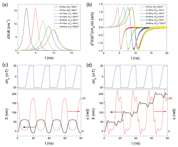
Figure 3. The dependence of domain wall motion on the ramp rate of the induced anisotropy. (a) The velocity (dX/dt) and (b) the acceleration, scaled by the rate of change of the induced effective field ((d2X/dt)/( )) of the domain wall as a function of time for different rates of inducing the anisotropy energy. (c) The domain wall position in response to an induced anisotropy energy sequence that provides a larger force on the negative anisotropy pulse (
 ) applied in 1 ns, than on the positive anisotropy pulse (
 ) ramped over 5 ns. In the absence of a pinning potential the anisotropy energy sequence causes the domain wall to move back and forth between the same two positions, resulting in no net movement. (d) In the presence of a periodic potential the anisotropy energy sequence causes a ratchet-like motion of the domain wall along the wire.
Download figure:
Standard image High-resolution imageConsidering a domain wall subjected to an alternating anisotropy energy in a nanowire with no mechanism to pin the domain wall position, then the domain wall will oscillate back and forth between the same two locations, irrespective of the magnitude of the force, with no net displacement over a full cycle of the anisotropy energy as shown in figure 3(c). However, in the presence of a spatially non-uniform anisotropy energy, with energy minima designed to pin domain walls (e.g. lithographically patterned notches or locally modifying the material properties [2, 22]), then it would be possible to induce a ratchet-like motion of the domain wall by ramping the anisotropy energy at different rates on the up and down cycles. We modelled the effects of pinning as a spatially dependent field component in the z-direction given by  , where w = 100 nm represents the wire width and
  with
with  J and
J and  = 30 nm. Similar parameters have been used previously to make qualitative predictions of the effects of pinning and thermal fluctuations in CoPtCr [15] and Pt/Co/Pt [16] layers.
As shown in figure 3(d), as the anisotropy energy is ramped at a fast rate, the induced force can be sufficient to overcome the spatially varying anisotropy profile, while the smaller force on the slower ramp results in pinning of the domain wall and therefore a net displacement over the full anisotropy energy cycle. The direction of the net motion of the domain wall would be reversed if the fast-negative/slow-positive pulse sequence was replaced by a fast-positive/slow-negative pulse sequence. Therefore, it should be possible to induce forwards and backwards displacement of the domain wall deterministically by tailoring the anisotropy pulse sequence.
Discussion
The possibility of moving domain walls along nanowires deterministically by tailoring an anisotropy pulse sequence has potential for applications in devices for information storage and processing. A promising route to a practical realisation would be in a hybrid piezoelectric/ferromagnet device as depicted in figure 1(b). The formation of a mesa in the piezoelectric layer would release clamping by the substrate and would allow the material to expand or contract in the direction perpendicular to the mesa in response to the voltage pulse applied to the electrodes fabricated along the sides. A magnetic nanowire fabricated on top of the mesa can support several magnetic domain walls distributed along its length. Typical material choices for magnetic materials with perpendicular magnetic anisotropy include heavy metal/ferromagnet/heavy metal stacks (e.g. Pt/Co/Pt). In such systems the Dzyaloshinskii–Moriya interaction (DMI), which arises at the heavy metal/ferromagnet interface, stabilises the Néel domain wall configuration with the same preferred chirality for up/down and down/up domain wall configurations [15, 16, 34]. This is a fortuitous situation for our design because it will ensure that domain walls in which the magnetisation rotates from up to down, or from down to up, move in the same direction for the same anisotropy pulse sequence. The ability to move a sequence of adjacent domain walls in the same direction by applying a single voltage pulse could make the method particularly relevant to a Racetrack type of memory device [2].
Possible choices for the piezoelectric material include PZT, PMN-PT or PZN-PT. In these materials it is possible to generate mechanical strains of order 10−4 to 10−3 for electric fields of order 1 MV m−1 [35], corresponding to 0.1 V applied across a 100nm wide mesa. Mechanical strain of this magnitude will induce magnetic anisotropy energy or field on the order of tens of kJ m−3 or mT [33], comparable to the values used in our calculations. The energy required to charge and mechanically deform the piezoelectric mesa will typically be is on the order of femto-Joules [23, 26]. In figure 4 we present the results of calculations made using the COMSOL Multiphysics package [36] to simulate the response to a voltage pulse of a 100 nm wide mesa fabricated in PMN-PT. The strain and energies are of the expected order and the calculations show that the strain can be generated on the sub-nanosecond timescale. To simulate the effect of a strain pulse on a domain wall in this device design we performed micromagnetic simulations using the object oriented micromagnetic framework (OOMMF) package [40]. Simulations were performed for a wire geometry with width = 40 nm, thickness = 1 nm and periodic boundary conditions along the length direction. The mesh size was 1 nm × 1 nm × 1 nm. Magnetisation, MS = 1400 kA m−1. The Gilbert damping parameter, α = 0.1. Perpendicular magnetic anisotropy was simulated using a uniaxial anisotropy constant,  . The in plane uniaxial anisotropy was simulated by fitting to the strain profile shown in figure 4(d) and converting this to a spatially dependent uniaxial anisotropy energy using a magnetoelastic coupling constant,
  , consistent with that found for Pt/Co/Pt layers in [41]. A static magnetic field of 10mT was applied transverse to the wire in order to keep the internal angle of the domain within the same quadrant and to prevent it from forming a purely Neel wall configuration. The resulting domain wall displacement is shown in figure 5, confirming the main finding of our manuscript, that a uniaxial anisotropy pulse will induce the displacement of a domain wall, and showing the expected magnitude of the displacement for realistic device parameters. Differences in the exact form of the displacement verses time obtained from the numerical calculations and the micromagnetic simulations arise from the fact that the micromagnetic simulations use the uniaxial anisotropy energy with a varying profile across the width of the wire, and also include dipolar and demagnetising fields.
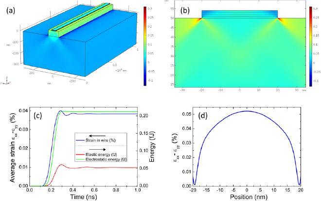
Figure 4. Simulations of the response to a voltage pulse of a mesa fabricated in a piezoelectric. (a) Transverse component of the in-plane strain (%) on the surface of the simulated structure; (b) transverse strain (%) at the cross-section of the mesa and the wire; (c) transverse strain averaged over the ferromagnetic layer of the wire as a function of time, and the electrostatic and elastic strain energies as functions of time plotted on the second vertical axis; (d) the strain as a function of position across the width of the Co layer 1ns after the pulse is applied. The simulated device consists of a 600 nm wide and 300 nm thick PMN-PT substrate, a 100 nm wide and 50 nm deep PMN-PT mesa, and a stack of four layers forming the wire: Pt/Co/Pt/Au. Each of the four layers is 40 nm wide and 1 nm thick. All components of the structure are 1 µm long. The voltage is applied to the sides of the mesa so that the electric field of 1 MV m−1 is parallel to the poling direction. The parameters describing the PMN-PT mesa were taken from [37] and its piezoelectric coupling constants were: d31 = −600 pC/N and d33 = 1400 pC/N. We assumed an elastic matrix of cubic symmetry for Au [38], Pt [39], and Co [39]. Our model approximates a wire of infinite length as we imposed zero displacement parallel to the wire at all boundaries perpendicular to the wire axis. The applied voltage starts rising smoothly at 0.1 ns and reaches the maximum value at 0.3 ns.
Download figure:
Standard image High-resolution image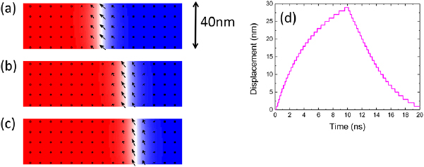
Figure 5. Results of micromagnetic simulations. (a)–(c) The magnetisation along the Co nanowire. Red (blue) represents magnetisation pointing out of (into) the page. The arrows show the in-plane direction of the magnetisation within the domain wall. The domain wall position is shown for a time (a) 0 ns, (b) 5 ns and (c) 10 ns after the application of an in-plane uniaxial anisotropy energy representing the strain profile depicted in figure 4(d). (d) The simulated domain wall displacement for a compressive strain pulse applied at 0 ns and a tensile strain pulse applied at 10 ns. The step-like appearance of the curve arises due to the finite mesh size used in the simulations.
Download figure:
Standard image High-resolution image
The fact that the proposed device avoids the use of energy dissipating electrical current makes it orders of magnitude more energy efficient than the pico-Joule operation of spin transfer torque driven racetrack memory, where comparable domain wall velocities, of order tens of ms−1, are achieved [42]. The domain wall velocities in our device can be increased by designing materials and nanowires to support wider domain walls with lower damping coefficients. The azimuthal angle rotates back and forth between Bloch and Néel states in response to anisotropy pulses of alternating sign, but does not rotate continuously, as in the case of field or current driven domain walls in the Walker regime [28–30]. In our case the domain wall velocity is determined by the magnitude of the anisotropy pulse and the rate at which the anisotropy can be varied.
The motion of the magnetic domain wall in response to the induced magnetic anisotropy energy occurs due to the fact that the magnetic free energy varies as a function of position across the domain wall. Therefore, one can expect that anisotropy pulses will influence the motion of other magnetic textures such as skyrmions, solitons and domain walls in materials with in-plane magnetisation and in antiferromagnets. The investigation of other magnetic textures will provide interesting avenues for further study.
In summary, we have introduced a method to control the motion of magnetic domain walls deterministically by inducing anisotropy energy pulses on timescales comparable to the magnetisation dynamics. We have analysed the dependence of the motion on the parameters of the magnetic material and on the anisotropy energy pulse profile. We considered the specific example of anisotropy energy created by a voltage pulse applied to a piezoelectric layer, and discussed in detail how it can be implemented in an ultra-energy efficient information storage device, but alternative methods to induce anisotropy pulses will act on the domain walls in the same way. Possible methods might include direct electric field gating, optical and heat pulses, and surface acoustic waves, and applications will range from information and communications technologies to motion sensing and to biomedical science.
Acknowledgments
This work was supported by the Engineering and Physical Sciences Research Council (Grant Nos. EP/H003487/1 and EP/K503800/1).