
Abstract
This work reports on the continuing development of a lab-on-a-chip electrochemical sensor for determination of zinc in blood serum using square wave anodic stripping voltammetry. The microscale sensor consists of a three electrode system, including an environmentally friendly bismuth working electrode, an integrated silver/silver chloride reference electrode, and a gold auxiliary electrode. The sensor demonstrates a linear response in 0.1 M acetate buffer at pH 6 for zinc concentrations in the 1–30 μM range. By optimizing bismuth film deposition and better control of the fabrication process, repeatability of the sensor was improved, reducing variability from 42% to <2%. Through optimization of electrolyte and stripping voltammetry parameters, limit of detection was greatly improved to 60 nM. The optimized sensor was also able to measure zinc in the extracted blood serum. Ultimately, with integrated sample preparation, the sensor will permit rapid (min) measurements of zinc from a sub-mL sample (a few drops of blood) for clinical applications.
Export citation and abstract BibTeX RIS
Conventional methods for determining trace level of zinc (Zn) are based on spectroscopy, including atomic absorption spectroscopy (AAS)1,2 and inductively coupled plasma mass spectrometry (ICP-MS).3,4 Both of these methods provide accurate measurements in diluted serum or blood, but require bulky and expensive instruments and specialized personnel to operate them. Furthermore, shipping of samples to a centralized lab can present significant time delays of potentially time-sensitive information. Due to these challenges, conventional methods are not suitable for bed-side monitoring of Zn level in blood for some patients in clinical settings, and thus, a low-cost point-of-care sensor with rapid response is in great demand.
Compared with spectroscopic methods, anodic stripping voltammetry (ASV) is a promising alternative for measurements of trace metals such as Zn.5,6 The analysis involves a negatively-biased preconcentration step to accumulate target metal ions onto an electrode surface by reducing them to their metal form, followed by a positively-scanned stripping step to re-oxidize the metals back to their ionic form. ASV is more time and cost effective than spectroscopic methods, offering limits of detection (LODs) in the sub-nanomolar range, which is sufficient for clinical measurements. Previous work has been mainly based on mercury electrodes due to the stable performance and low LODs,7–10 but handling and disposal issues stemming from mercury toxicity impede widespread application.
Bismuth (Bi) has been gaining popularity in recent years as an alternative electrode material for electrochemical measurements. It forms low-temperature alloys with heavy metals to enable preconcentration and offers a wide negative potential window. Most importantly it is much less toxic than mercury, making it more environmentally-friendly.11 Wang et al.12 compared the performance of in situ deposited Bi films on carbon-based electrodes to mercury film electrodes (MFE) for ppb level Zn measurements in acetate buffer and found responses to be comparable.
We recently reported on the development of a miniaturized lab-on-a-chip sensor with an electrodeposited Bi thin film electrode for measuring Zn (Fig. 1a).13,14 Our sensor size is approximately 15 mm × 19 mm, requires only microliters of sample, and performs an analysis in less than 15 min. These features make it ideal for point-of-care applications. The sensor consists of a gold (Au) auxiliary electrode (AE), a silver/silver chloride (Ag/AgCl) reference electrode (RE) and a Bi working electrode (WE) (Fig. 1b). When detecting Zn, the metal ion is first deposited from sample onto the Bi WE surface, and is stripped from the electrode by a potential scan to oxidize it back to its ionic form. The resulting current signal is proportional to Zn concentration in the sample (Fig. 1c). In our system, the preconcentration step was performed at −1.6 V, which is sufficiently negative of the Zn stripping peak at −1.3 V to ensure metal deposition. Following every Zn measurement, we stripped the Bi film from the WE surface by scanning positively beyond its stripping peak at −0.3 V, and electrodeposited a fresh Bi layer immediately prior to the next analysis. This strategy was followed to prevent fouling and provides a fresh electrode surface for repeated analyses.
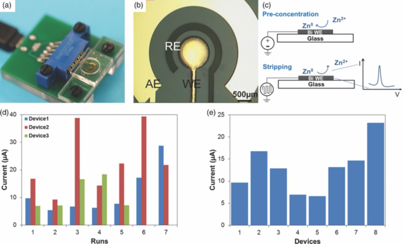
Figure 1. (a) Photograph of the sensor with an interface for potentiostat connection. (b) Close-up of the electrochemical cell, illustrating configuration of the electrodes. (c) Schematic illustrating the ASV process. (d) Variation in peak current in repeated analysis on the same device. (e) Variation in peak current in repeated analysis using the first run of different devices. ASV performed in 20 μM Zn, 0.1 M acetate buffer (pH 6). Preconcentration potential −1.6 V, duration 600 s, amplitude 25 mV, period 70 ms, increment 4 mV.
Despite being able to successfully detect and quantify Zn in the physiologically-relevant concentrations range of 65–95 μg/dL (10–15 μM),15 we found reproducibility of sensor response to be a critical challenge. Fig. 1d illustrates variability in repeated measurements of 20 μM Zn in 0.1 M acetate buffer (pH 6) using the same device, repeated in triplicate. The measured peak current varies by as much as 30 μA or up to 4× of the initial value for repeated measurements on the same device. The underlying reason for this, as we found, is that Bi complexes with Au (most likely forming an alloy), making it impossible to strip off Bi completely from the underlying Au surface simply by applying a more positive potential, suggesting that sensors with electrodeposited Bi WEs cannot be easily reused. Using sensors only once (i.e., disposable) improved performance substantially. However, variability sill remained high (Fig. 1e), with peak currents ranging from 6 to 23 μA.
In this work, we focused on improving reproducibility of our lab-on-a-chip sensor. By optimizing the electrodeposition of Bi film and better control of fabrication steps, repeatability of the lab-on-a-chip sensor was improved. These improvements were evaluated from both device fabrication and electrochemical performance points of view. Through these optimization steps, sensor LOD was greatly improved, while substantially reducing variability of measurements.
Experimental
Reagents and chemicals
We purchased all chemicals from Fisher Scientific, unless stated otherwise, and prepared reagents as follows. Piranha solution to clean glass substrates was prepared from H2SO4 and H2O2 in 7:3 v/v ratio. Sulfuric acid (ACS grade, 98%) was purchased from Pharmco-AAPER. Peroxide (30%) was purchased from J.T.Baker. Au etchant was prepared from I2, KI, and DI water in 4:1:40 w/w/v ratio. Titanium etchant was made from HNO3, HF and DI water in 1:2:7 v/v/v ratio. Bi target (Bi pieces, 1-12 mm, 99.999% trace metal basis) was purchased from Sigma Aldrich. Ag plating solution (Silver Cyless II) was purchased from Technic Inc., and a 1 M KCl solution was prepared from salt. Acetate buffer (pH 4.65, 0.1 M) was purchased from Fluka and adjusted to pH 6 with NaOH and acetic acid (Fisher Scientific). Bi stock solution (AAS Standard, 1000 mg/L in 2% nitric acid, Fluka) and Zn stock solution (AAS Standard, 1000 mg/L in 2% nitric acid, Fluka) were purchased from Sigma Aldrich. Hyclone Characterized Fetal Bovine Serum was purchased from Thermo Scientific.
Device design and fabrication
The sensor was fabricated using a combination of lithographic and deposition techniques (Fig. 2). Metal layers of 20 nm titanium/200 nm Au were evaporated on glass slides cleaned by piranha etching. Three electrode patterns with contact pads were formed using photolithography and etching. A Ag/AgCl RE was fabricated by electroplating Ag on Au seed layer using 3 mA/cm2 cathodic current density for 60 s, and chloridizing the Ag in 1M KCl using the same anodic current for 30 s. Different deposition parameters for electroplating Bi WE were investigated to obtain a better-performing sensor, and were finally optimized using chronoamperometry in 500 mg/L Bi (0.01 M acetate buffer, pH 4.65) at −0.8 V for 240 s followed by rinsing with DI water for 60 s. The electrode layout is shown in the photograph of a completed sensor in Fig. 1b. In addition to electroplating, evaporation was also used for deposition of the Bi WE. For evaporated Bi WE, a second photolithography step was used to form the WE pattern. A 200 nm Bi layer was evaporated on Au, and then photoresist with Bi was lifted off.
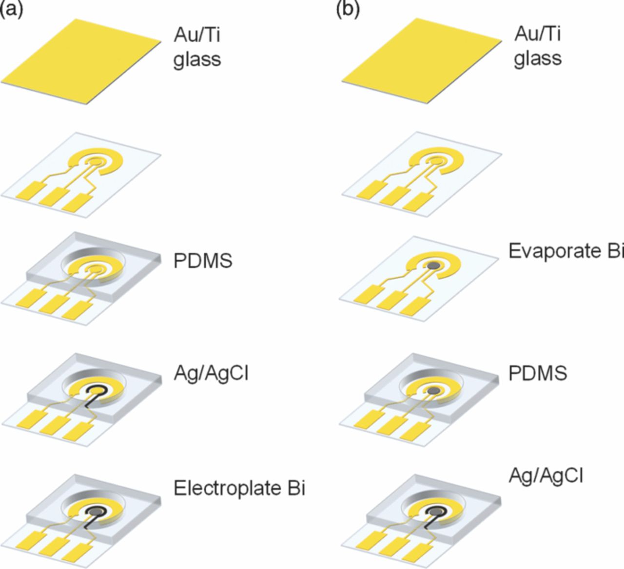
Figure 2. Sensor fabrication process. Bi WEs were formed by either (a) electroplating or (b) evaporation.
A polymer well was fabricated in polydimethylsiloxane (PDMS) using standard soft lithography methods, making it compatible with future integration of microfluidics. It was bonded to glass substrate contacting the electrode patterns using air plasma discharge. An interconnect was fabricated using PCB board to facilitate connection between sensors and potentiostat. An edge board connector matching electrical pad geometry of the sensor and a mini USB port were soldered on the PCB interconnect. To perform electrochemical experiments, as shown in Fig. 1a, the sensor was inserted into the edge board connector, and connected to the potentiostat through a mini USB cable.
Electrochemical experiments
A portable potentiostat (WaveNow, Pine Instrument) was used to perform electrochemical experiments. Cyclic voltammetry was initially performed in 0.1 M acetate buffer (pH 4.65) to determine potential windows for different WEs. ASV (Fig. 1c) was performed in samples of 100 μL containing Zn of different concentrations in acetate buffer (0.1 M, pH 6). Preconcentration was carried out at a potential of −1.6 V and duration of 600 s. Square wave voltammertry was used for the stripping step. The waveform parameters were as follows: 25 mV amplitude, 70 ms period, and 4 mV increment. The scan range was from −1.6 V to −0.6 V. To evaluate repeatability of different sensors, a minimum of three sensors of the same type were used to quantify 20 μM Zn. Calibration curves were constructed for sensors containing electroplated or evaporated Bi WEs in the concentration range of 1–30 μM Zn.
Serum pretreatment
Serum was diluted by acetate buffer (0.1 M, pH 6) with different dilution factors. The extraction procedure developed earlier was followed.16 First, 10 mL (5 mM) dithizone in chloroform was deprotonated by mixing with 10 mL (pH 9) 1 M ammonia/0.5 M ammonium buffer solution. Then the deprotonated form of dithizone was mixed with the solution containing serum and 0.5 mL of 0.05 M potassium thiocyanate in ethanol, followed by sonication for a period of 5 min. Afterward, the solution was transferred into a 50 mL plastic tube and centrifuged for 10 min at a rate of 4000 rpm to separate the two phases. The organic phase was collected and sonicated with 10 mL of 1 M sulfuric acid for another 5 min. After the extraction procedures, we adjusted the pH of the sample to 6 using NaOH and diluted the sample with acetate buffer (0.1 M, pH 6) by a factor of 2.
Results and Discussion
Improving Bi working electrode
We carefully examined electrodeposition of Bi films to improve sensor performance. In our earlier work,13,14 we electrodeposited Bi at −0.8 V for 240 s. The Bi film was approximately 160 nm thick with surface roughness of 230 nm. While the Bi film covered the Au surface completely, Bi tended to aggregate along the edge, forming mesh-like branches that extended into the gap between WE and RE. This caused variations in Zn accumulation on the WE during deposition due to variability in surface area. When this Bi film was used for Zn ASV determination in acetate buffer, it exhibited high LOD of 6 μM, and it could only provide measurements in serum samples spiked with 20–60 μM of Zn.13
To reduce surface roughness of the Bi film and improve repeatability of the sensor, we optimized the fabrication procedures. Plasma treatment is a standard process in bonding of PDMS to glass in soft lithography. In our earlier work,13,14 we applied plasma to the PDMS layer for 20 s and to the glass slide with electrode patterns for 5 s. However, we found that plasma could damage the thin Au film defining electrodes so severely that the edges of the electrode turned porous. Thus, the process was revised to include plasma application to the PDMS layer only, which eliminated Au electrode degradation.
While it is a common practice to stir solution during electrodeposition to enhance mass transport, we found that using quiescent solution yielded more consistent Bi films with smoother surfaces and cleaner edges. We also deoxygenated the Bi plating solution 17,18 to achieve better film quality and reduce surface roughness. Overall, making these modifications proved critical to improving consistency of device manufacturing and ultimately device performance. The Bi film after optimization was approximately 200 nm thick with surface roughness of 130 nm. However, Bi still tended to aggregate along the edge (Fig. 3a, 3c), forming extra mesh-like branches that extended into the gap between WE and RE. This undesirable accumulation of Bi, which we attribute to a combination of factors (enhanced mass transport at the edges, deposition kinetics, and larger electric field along the edge of the WE due to cell geometry) was unavoidable as long as the distribution of surrounding electrolyte and mass transport do not change. To avoid this problem, we explored another, non-electrochemical deposition technique.
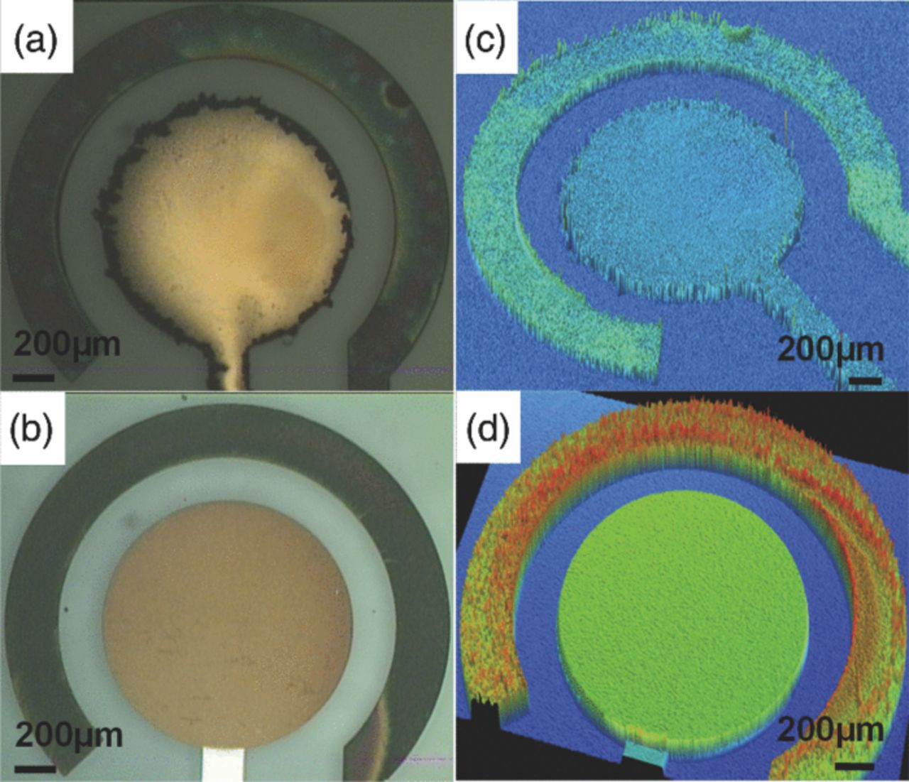
Figure 3. Comparisons of surface morphologies of electroplated (top row) and evaporated (bottom row) Bi WEs: (a-b) microscopic photos and (c-d) optical profiler scans of each type of Bi WEs, respectively.
To further improve film quality, we directly evaporated Bi on Au (Fig. 2b), which was expected to yield film of the highest quality possible. Electrode pattern was formed using the lift-off process, to guarantee a clean edge for the WE. The Au surface was evenly covered by 300 nm of Bi, with few defects and surface roughness of 40 ± 2 nm. The value of surface roughness indicated the evaporated Bi surface was smooth and comparable to the patterned Au with surface roughness of 15 nm. Considering the aggregation associated with electroplated Bi (as seen in Fig. 3b, 3d), the evaporated Bi electrode offers a uniform surface from center to edge of the electrode, which is a significant improvement over the electroplated Bi electrode.
We used cyclic voltammetry (CV) to examine both types of Bi WEs and compare with a Au WE. Au electrode was chosen since it is a commonly used electrode material in electrochemistry and is the seed layer beneath both Bi films. One of the most useful parameters in comparing WEs is potential window, which defines the range of potentials that the electrode is capable of supporting before onset of reduction of water. Potential window can be influenced by a number of parameters, including electrode composition and surface, electrolyte composition and pH value. The potential window of the Au WE is sufficiently wide to detect Pb and Cd, while Bi deposited on carbon-based electrode has been demonstrated to have an even wider window, which is important for metals with more negative potentials such as Zn.12
Cyclic voltammetry was performed in acetate buffer (0.1 M, pH 4.65) with different WEs, as shown in Fig. 4a. The significant increase in current at increasingly negative potentials indicates reduction of water, which leads to degradation of the electrode film and hydrogen gas evolution on the AE. Fig. 4b shows the negative threshold potentials of three electrodes at 10 μA, which is typical of ASV analysis. Considering that Zn exhibits a stripping peak at approximately −1.35 V, electroplated Bi with a threshold potential of −1.4 V makes it a suitable WE material. The threshold potential of evaporated Bi is −1.2 V, while the Zn stripping peaks on evaporated Bi shift to approximately −1.2 V (as we will discuss below), which makes it also suitable. Au, with the most positive threshold potential of −1.1 V, does not have the range for Zn detection, as substantial increase in current due to reduction of water will drown the Zn stripping signal. On the positive potential side, Au has wider window for metals like Cu while Bi strips off at a potential more positive than −0.3 V. The potential window of the electroplated Bi WE offers the widest analysis window for Zn determination.
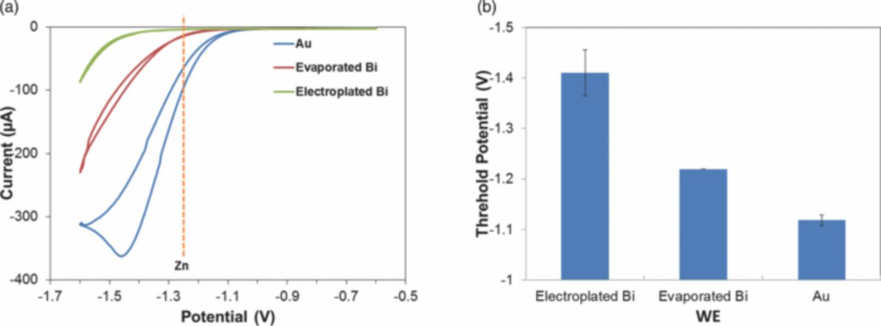
Figure 4. (a) Potential windows of electroplated and evaporated Bi, and Au WEs, with microfabricated Ag/AgCl RE and Au AE. Cyclic voltammetry performed in 0.1 M acetate buffer (pH 6) with scan rate 100 mV/s. (b) Threshold potential (i = 10 μA) of different WEs.
Comparing the two types of Bi WEs, both are advantageous, depending on perspective. Electroplated Bi WE has a wider potential window than evaporated Bi, while both are sufficiently wide for detection of Zn. From surface quality perspective, evaporated Bi WE is a more uniform film than the electroplated Bi, thus offering better repeatability and lower LOD. However, from the fabrication complexity perspective, evaporated Bi WE is more complex due to additional photolithography and Bi evaporation steps. The simpler fabrication process (and ultimately lower cost) of the electroplated Bi WE make it more suitable for disposable applications. Therefore, a trade-off between fabrication complexity and surface consistency must be considered based on the demands of the target application. To further evaluate and contrast the two Bi film electrodes, electrochemical performance in metal stripping must be considered, as we discuss below.
Calibration in acetate buffer
To compare the electrochemical performance of both Bi electrodes, square wave ASV (SWASV) of Zn in the 1–30 μM range was performed in acetate buffer. The representative results are shown in Fig. 5. The range was selected to bracket the physiological range of Zn in serum, which is approximately 10–15 μM.15 The buffer (0.1 M, pH 6) and deposition parameters (600 s at −1.6 V) were optimized in our previous work.13 For the electroplated Bi WE, Zn stripping peak occurred at −1.34 V (Fig. 5a), which is approximately at the same potential as obtained with our previous electroplated Bi WE. For the evaporated Bi WEs, Zn stripping peak appears at −1.1 V for lower concentrations (Fig. 5b), which is ∼250 mV more positive than the electroplated Bi WEs. One possible reason for this is due to differences in fabrication, which may bring different Cl- concentrations and therefore the potentials of REs. Another possible reason is due to surface roughness differences, e.g. the potential may shift as much as on carbon-based electrodes with different surfaces.19 Nevertheless, as long as the potential for Zn stripping peak is fixed, there is no effect on the peak height we measure for calibration. Another observation is that with increasing concentration, Zn stripping peaks on evaporated Bi WEs shift more negatively to −1.25 V. This is most likely the consequence of using solid film electrodes, causing Zn to deposit on Bi first, with additional Zn depositing on the Zn monolayer, which requires less energy to strip off.20 While with rougher electroplated surface, Zn is always deposited on Bi so that the potential remains the same in the whole range.
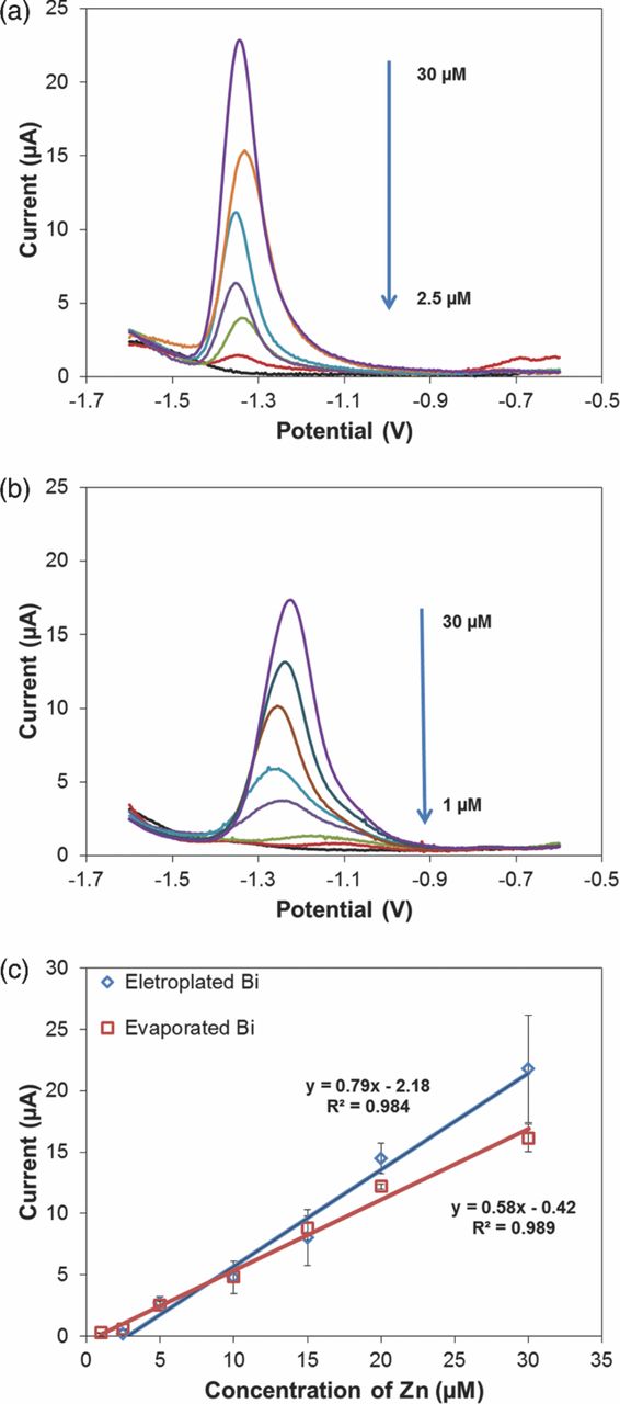
Figure 5. ASV of Zn (a) in the 2.5–30 μM range using electroplated Bi WE and (b) in the 1–30 μM range using evaporated Bi WE. Analyzes performed in acetate buffer (0.1 M, pH 6), 100 μL sample. Preconcentration potential −1.6 V, duration 600 s, amplitude 25 mV, period 70 ms, increment 4 mV. (c) Calibration curves for Zn in buffer using Bi WEs.
Calibration curves for both Bi electrodes, constructed using Zn peak currents, show linear performance over the target concentration range (Fig. 5c). The electroplated Bi electrode exhibited higher sensitivity to Zn in acetate buffer than the evaporated electrode (0.79 μA/μM vs. 0.58 μA/μM, respectively). However, the electroplated Bi WEs exhibited a lower LOD than the evaporated sensors (calculated as 130 nM vs. 60 nM, respectively) based on 3σ/slope (n = 5). The lowest measured concentrations for each electrode were 2.5 and 1 μM, respectively. Compared with the sensors we reported previously,13 the lowest measured concentration improved from 5 μM, while the sensitivity decreased from 1.48 μA/μM. The improved LOD is most likely the benefit of the fabrication process optimization, which yielded more uniform films. However, the resulting smoother films are the most likely reason for the lower sensitivity, as this translates into lower surface roughness and thus reduced surface area of the electrode.
To demonstrate the improvement in electrochemical performance of the Bi WEs, we compared the electrodes based on their ability to determine Zn. Fig. 6 illustrates reproducibility of the electrodes in repeated stripping analyzes of a sample containing 20 μM Zn in 0.1 M acetate buffer (pH 6). In both cases the same stripping parameters were used (preconcentration at −1.6 V for 600 s, stripping waveform amplitude 25 mV, period 70 ms, increment 4 mV). The measured peak current was 14.5 ± 1.2 μA for the electroplated Bi electrode and 12.2 ± 0.2 μA for the evaporated Bi electrode. Compared with the results from the first-generation Bi film electrodes, the improved Bi electroplating procedures created smoother and higher-quality films, leading to a small increase in the Zn peak current from 13 μA to 14.5 μA. But most importantly, these improvements were accompanied by a dramatic drop in measurement variability, from 42% to 8%. For the E-beam evaporated Bi films, the peak amplitude of the signal current declined to ∼12 μA due to the large decrease in film roughness, which affects the available electrode surface area. The measurement variability for this electrode improved more substantially, decreasing to less than 2%.
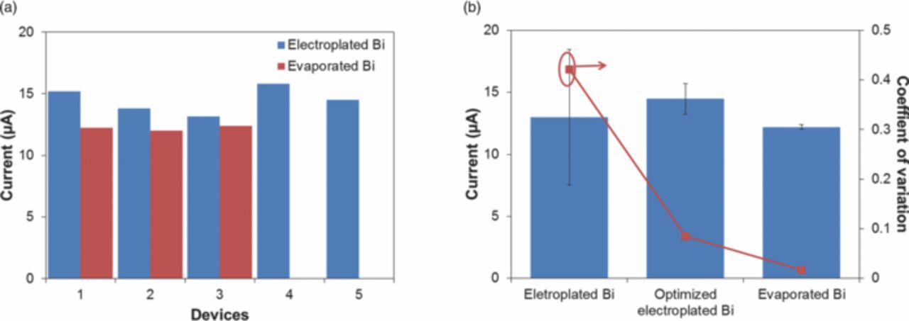
Figure 6. (a) Variations of peak currents in the first run of electroplated and evaporated Bi WEs. (b) Improvement of repeatability of sensors with electroplated Bi WE before and after optimization of fabrication procedure, and evaporated Bi WE. ASV performed repeatedly in 20 μM Zn, 0.1 M acetate buffer, pH 6 (n = 5 for electroplated Bi, n = 3 for evaporated Bi). Preconcentration potential −1.6 V, duration 600 s, amplitude 25 mV, period 70 ms, increment 4 mV.
The improvement in measurement variability is even more impressive when compared with the well-accepted commercial LeadCare system (LeadCare II, Magellan Diagnostics). Similar to our sensor, the LeadCare system is based on ASV as well, but is used for the determination of Pb content in whole blood. The system variability is approximately 8%.21 A well-accepted gold-standard for trace metal analysis, ICP-MS, generally exhibits an intra-assay variability for Zn measurements in plasma of 0.27%22 and inter-assay variability of 2.4%. Our results suggest that performance of our Bi WE sensors is comparable, and in the case of evaporated Bi WE is superior to that of a commercial system, approaching that of a laboratory-scale ICP-MS instrument.
Analysis in diluted serum
There is a great demand for bed-side monitoring of Zn levels in serum in clinical settings. Pediatric and adult studies have consistently demonstrated abnormally low Zn levels in critically ill patients.23–26 While Zn homeostasis can be easily restored though Zn supplementation,27–30 excess Zn intake can lead to copper deficiency and neurologic disease such as myelopathy or Alzheimer's.31–33 For such patients, careful monitoring of Zn levels in serum becomes of critical importance. Due to challenges and complexities of conventional methods, ASV is a promising alternative that is easier to miniaturize for point-of-care measurement of Zn.
The determination of Zn in serum is a critical challenge for ASV sensors since the technique only measures free metal ions, while as much as 60% of Zn in serum may be bound by protein.34 Thus, direct measurement of Zn in serum or diluted serum is impossible when LOD of the sensor is on the same order of magnitude as metal concentration, as was the case with our first generation Bi WE sensor.13 With a substantially improved LOD, nearly 100× lower than the typical range of Zn in serum, it may now be possible to directly measure free Zn in serum. Such a measurement could provide additional information for clinicians, since the current ICP-MS based Zn detection is only capable of providing the total Zn concentration. One reason such measurements are of interest is that free Zn is bio-available and may exhibit better correlation with medical conditions, similar to Ca2+ for which the concentration of free ions is more important to consider than total concentration.35 Another motivating factor for direct measurements in serum is that sample preparation method, such as digestion and extraction, can be complex and time consuming. Considering the simplicity of sample preparation by dilution with buffer over digestion or extraction, it is worthwhile to investigate if free Zn ions can be detected in diluted serum directly.
We began by investigating the relationship between dilution factor and the sensor's performance. If the dilution factor is too small, the complexity of the serum sample matrix will still be dominant and will require the additional digestion or extraction steps. Conversely, a large dilution factor would lead to lower Zn levels and would require even lower detection limits. Thus, we first began with a 10× dilution. Unfortunately, no Zn peak could be measured. Fig. 7a illustrates peaks obtained when diluted serum was spiked with additional 20–60 μM of Zn. One interesting observation is that the peaks occur at −1.25 V, which is 100 mV more positive than in buffer. This shift is attributed to the differences in the concentration of Cl− in the two matrices, which affected the half-cell potential of the RE. The peak current for the 20 μM spiked sample was 0.84 μA, which is 6% smaller than in buffer. These results suggest that with the 10× dilution, the protein components of serum are still able to greatly affect the ASV process.
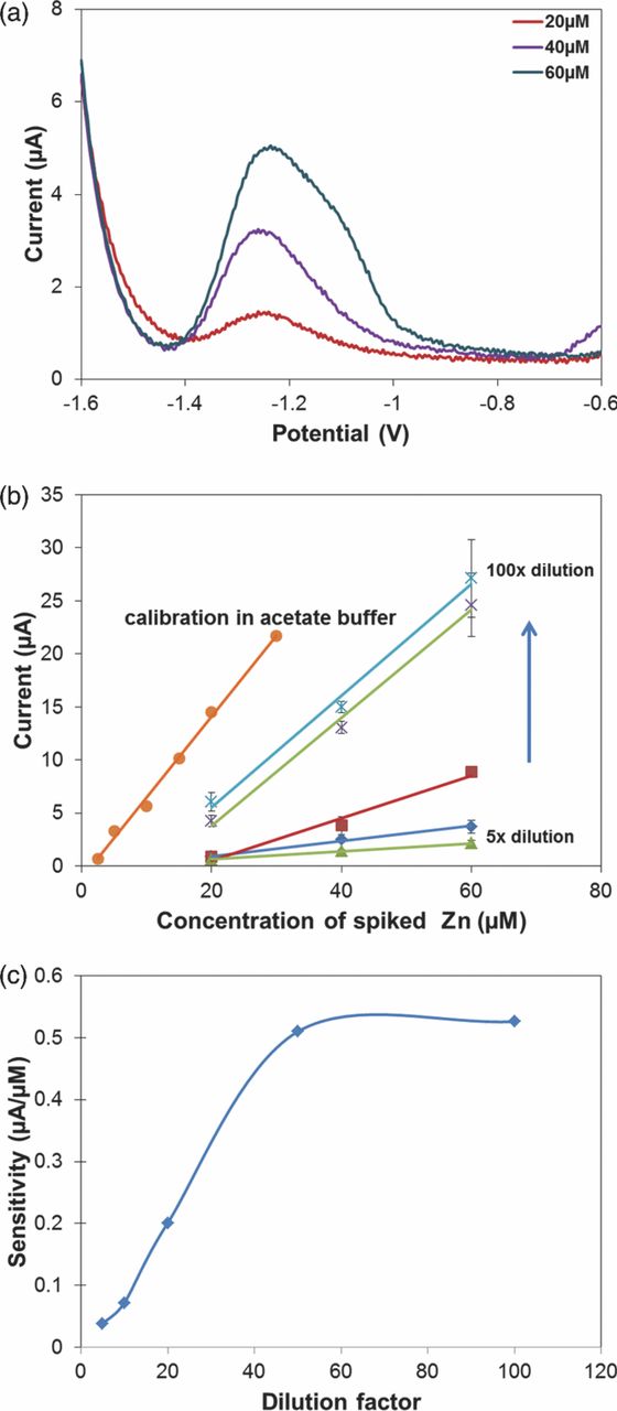
Figure 7. (a) ASV of diluted (10×) serum spiked with 20–60 μM of Zn using electroplated Bi WEs, 200 μL sample. Preconcentration potential −1.6 V, duration 600 s, amplitude 25 mV, period 40 ms, increment 4 mV. (b) Calibration curves for Zn in diluted serum with dilution factor from 5× to 100×. (c) Relationship between sensor sensitivity and dilution factor of serum.
Next, we performed further testes in serum spiked with 20–60 μM of Zn and diluted in the range of 5–100×. The results show that as the dilution factor increases (Fig. 7b), the striping peak current increases as well, although remains at much lower current levels than the corresponding concentrations in buffer. For example, the peak current for 20 μM in 100× diluted serum was 6 μA, which is 7× larger than that in 10× diluted serum and more than 40% smaller than that in buffer. Variability of the signal exhibited a decreasing trend with increasing dilution factor. For example, variability for 20 μM in 100× diluted serum has CV = 14.4%, which is almost 50% better than the 10× diluted serum, but it is higher than that of the buffer (CV = 8%). Plotting sensitivity of the sensor as a function of dilution factor reveals a saturation behavior (Fig. 7c). In the linear region, the sensor exhibits increase in sensitivity of approximately 1 nA/μM per 1× increase in dilution, until saturation at 50× dilution. At 50× dilution and above, sensitivity of the sensor saturates at 0.5 μA/μM, indicating that further dilution no longer reduced surface fouling. Nevertheless, these saturation values are still below the 0.79 μA/μM sensitivity exhibited in the buffer. These experiments suggest that a more complex pretreatment of serum, such as extraction, is necessary for this application.
Analysis of extracted serum
There are a number of options for pretreatment of serum for electrochemical trace metal detection. Digestion of serum is the easiest approach, and will break up proteins and release Zn sequestered within their structure. We found that the commercial product Metexchange36,37 originally developed for ASV detection of Pb, did not work for Zn. While the commonly-used method of acidification by HCl to digest serum worked, the results were not impressive as only spiked samples could be measured and it was impossible to calculate concentration of Zn in the original sample.13 Thus, a more complex approach that is able to extract metal ions from proteins and remove proteins by phase separation is needed. Herein, we developed a double extraction procedure which recovers 97% Zn16 in serum by ASV detection.
To demonstrate Zn determination in extracted serum, we used the evaporated Bi WE due to its superior reproducibility and lower coefficient of variation. In these experiments, repeatable Zn stripping peaks appear at −0.7 V (Fig. 8). By manually shifting the voltammograms in buffer 450 mV positively, the Zn peaks and background currents in the two matrices correlate. The shift is primarily attributed to the differences in the concentration of Cl− in the two matrices, which affected the half-cell potential of the RE. This experiment demonstrates that we can use evaporated Bi WE to detect Zn in un-spiked extracted serum. With further optimization of experimental parameters and the standard addition approach, we expect to be able to determine Zn levels in extracted serum.
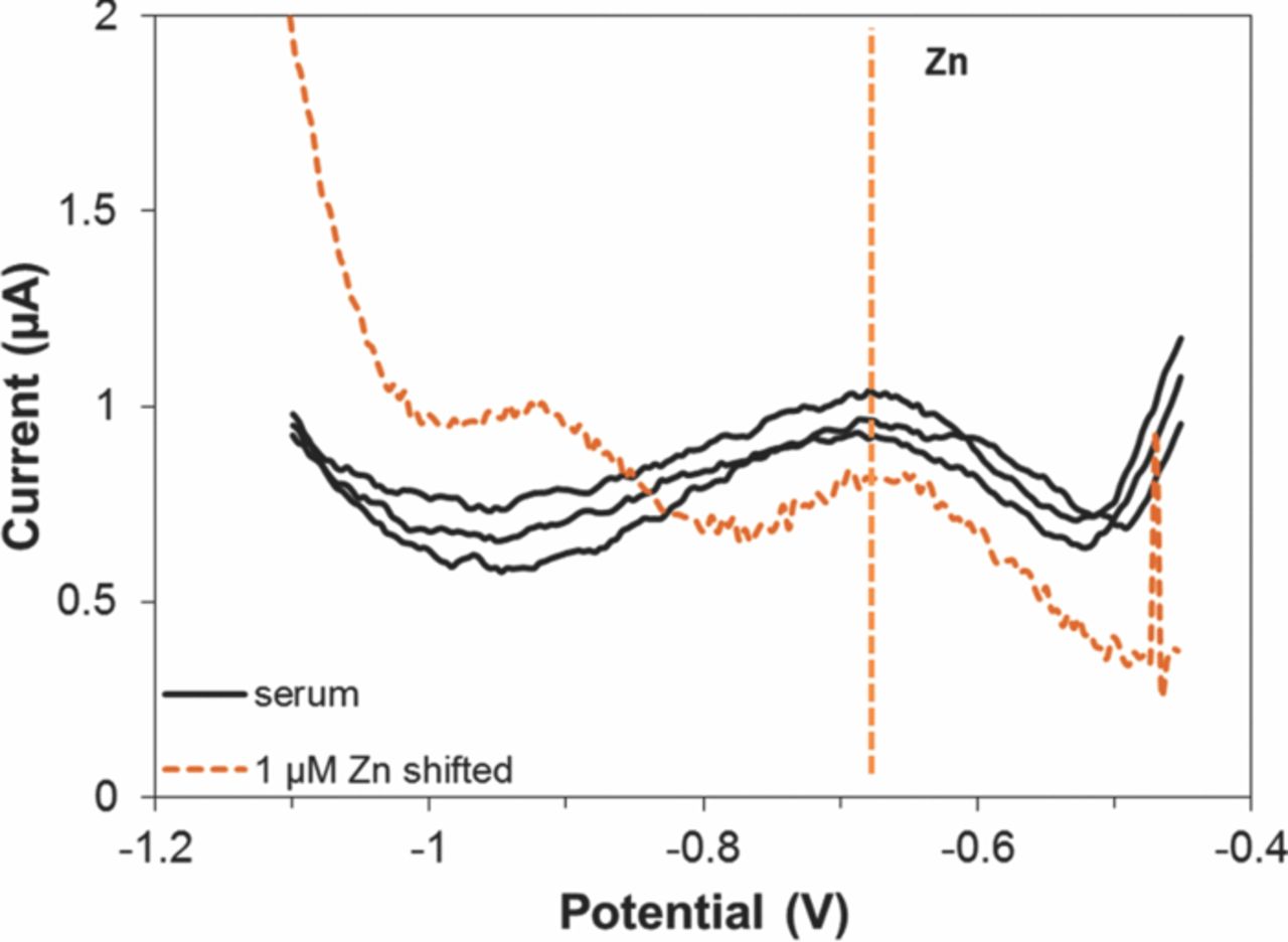
Figure 8. ASV in extracted serum using evaporated Bi WEs, 200 μL sample. Preconcentration potential −1.4 V, duration 900 s, amplitude 25 mV, period 40 ms, increment 4 mV.
Conclusions
In this work, we improved performance of Bi WEs by optimizing fabrication steps for electroplated and evaporated Bi WEs. Both electrodes have their advantages. From the fabrication perspective, the electroplated Bi WE offers a simpler fabrication process and thus lower cost. Conversely, the fabrication process for the evaporated Bi WE is more complex due to additional photolithography step and Bi evaporation steps. Thus, the electroplated Bi WE is more suitable for disposable point-of-care applications.
From the electrochemical performance perspective, however, the evaporated Bi WE offers superior consistency, and thus better repeatability (CV = 1.7%) and lower LOD (60 nM). More importantly, evaporated Bi WE is able to provide stable, repeatable measurements of Zn in extracted serum. For the electroplated Bi WE, both variability (CV = 8.5%) and LOD (130 nM) are higher than that of evaporated films, and measurements in extracted serum are not reliable. This leads us to conclude that from the electrochemical prospective, the evaporated Bi WE is superior. Ultimately, selection of the Bi electrode is dependent on the intended application. For our application of Zn measurement in serum, we prefer to use the evaporated Bi WE despite of the complexity of fabrication. The electroplated Bi WE, however, may be more favorable in other applications, where low-cost is critical and analyte concentrations are relatively high, such as determination of Pb or Zn in environmental water samples. In the future, we plan to continue development and optimization of the lab-on-a-chip sensor for determination of a variety of metals with negative stripping potentials in a wide range of sample matrices.
Acknowledgments
This work was supported in part by funds provided by the National Institutes of Health (NIH) grants R21ES019255 and R01ES022933, and the Ohio Center for Microfluidic Innovation.