
Abstract
Nanoscale scanning electrochemical microscopy (SECM) has emerged as a powerful electrochemical method that enables the study of interfacial reactions with unprecedentedly high spatial and kinetic resolution. In this work, we develop carbon nanoprobes with high electrochemical reactivity and well-controlled size and geometry based on chemical vapor deposition of carbon in quartz nanopipets. Carbon-filled nanopipets are milled by focused ion beam (FIB) technology to yield flat disk tips with a thin quartz sheath as confirmed by transmission electron microscopy. The extremely high electroactivity of FIB-milled carbon nanotips is quantified by very high standard electron-transfer rate constants of ≥10 cm/s for Ru(NH3)63+. The tip size and geometry are characterized in electrolyte solutions by SECM approach curve measurements not only to determine inner and outer tip radii of down to ∼27 and ∼38 nm, respectively, but also to ensure the absence of a conductive carbon layer on the outer wall. In addition, FIB-milled carbon nanotips reveal the limited conductivity of ∼100 nm-thick gold films under nanoscale mass-transport conditions. Importantly, carbon nanotips must be protected from electrostatic damage to enable reliable and quantitative nanoelectrochemical measurements.
Export citation and abstract BibTeX RIS
The development of nanometer-sized carbon electrodes is pivotal for various electrochemical applications including scanning electrochemical microscopy (SECM).1,2 Originally, carbon nanoelectrodes were fabricated by exposing the sharp tip of an etched carbon fiber from an insulating sheath. Frame-etched carbon nanoelectrodes3,4 were developed to detect neurotransmitters released from single vesicles at single cells5 and synapses.6 Electrochemically etched carbon nanoelectrodes7 were employed as non-catalytic conductive supports of single platinum nanoparticles to study their electrocatalytic activities.8 Etched carbon-fiber nanoelectrodes, however, yielded only low SECM feedback responses9 because of the conical tip geometry.10,11 Alternatively, disk-shaped carbon nanoelectrodes12 were developed by pyrolytic deposition of carbon.13 Heat-pulled quartz nanopipets were filled with pyrolytic carbon for single-cell imaging14–16 and were further modified with platinum for intracellular oxygen monitoring,17 iridium oxide for pH mapping,18 or mercury for stripping voltammetry of lithium ion.19 Pyrolytic carbon nanoelectrodes, however, demonstrated low feedback responses that poorly fit with SECM theory for inlaid disk tips.14–17
Recently, selective chemical vapor deposition (CVD) of carbon in quartz nanopipets enabled the development of carbon nanoelectrodes with controlled geometries.20,21 With this method, carbon is deposited more readily on the inner wall of a nanopipet than on its outer wall, because carbon sources (e.g., methane) are effectively trapped in the tapered nanopipet to ensure their frequent collision with the inner wall for carbon deposition.22 Moreover, a precise amount of carbon can be deposited by adjusting the duration of the CVD process to control the tip geometry. Short deposition results in the coating of the inner wall of a nanopipet with a thin carbon film, producing a carbon nanopipet that can be filled with an electrolyte solution for resistive-pulse sensing.23 Long deposition completely fills a nanopipet with carbon, with the exception of the tip, which was used as a nanocavity for sampling attoliter-to-picoliter volumes of electrolyte solutions24 or was platinized for oxygen sensing.25 Longer deposition yields a slightly protruded carbon tip to support single gold nanoparticles for the study of their electrocatalytic activity.26
Here, we report on CVD-based carbon nanoelectrodes with high electrochemical reactivity and well-controlled size and geometry for nanoscale SECM27 to enable reliable and quantitative nanoelectrochemical measurements. The intrinsically high electrochemical reactivity of CVD carbon24–26 is advantageous to electrolyze efficiently a redox species under the extremely high mass-transport conditions of nanoscale SECM. Geometrically, the thin quartz sheath of nanopipet-supported CVD carbon facilitates the close approach of its nanotip to the surface of a target substrate without a tip–substrate contact, which is a prerequisite for enhanced spatial and kinetic resolution of nanoscale SECM. The tip of nanopipet-supported CVD carbon, however, is not sufficiently flat because of the nanoscale protrusion or recession of carbon from the quartz sheath and the nanoscale roughness of both carbon and quartz tips. Mechanical polishing can smoothen successfully only the extremely small tips of CVD-carbon-filled nanopipets with radii of <5 nm, which were too small for SECM-based characterization.26
In this work, we mill the tips of CVD-carbon-filled quartz nanopipets by focused ion-beam (FIB) technology28,29 in order to yield flat tips with inner and outer radii of down to ∼27 and ∼38 nm, respectively. Advantageously, the thin quartz sheath allows for high-resolution transmission electron microscopy (TEM) imaging of the flat and sharp carbon nanotips. The geometry of FIB-milled carbon nanotips is well-controlled not only to quantitatively assess their remarkably high electrochemical reactivity, but also to yield high feedback responses in SECM approach curve measurements in contrast to previously reported carbon nanotips.9,14–17 Good agreement between experimental and simulated approach curves at SiO2-coated silicon wafers reliably confirms the well-characterized tip geometry and size, and a lack of a conductive carbon film on the outer tip wall. Moreover, an approach curve at a gold-coated silicon wafer shows a higher positive feedback response as the concentration of a redox mediator is lowered, thereby revealing the limited conductivity of the thin gold film under high mass-transport conditions across carbon–gold nanogaps. Importantly, we enabled reliable and quantitative nanoelectrochemical measurements by protecting carbon nanotips from nanoscale electrostatic damage,30,31 unlike the recent study of pyrolytic carbon nanoelectrodes.17
Theory
Here, we simulate SECM approach curves for a disk-shaped tip with a conductive outer wall for the first time to find that feedback responses are useful to assess the conductivity of the outer wall. In our model, the unbiased outer wall that is disconnected from the conductive tip serves as a bipolar electrode,32 where the product of a tip reaction, R, is electrolyzed to an original redox species, O, to affect the tip current not only in the bulk solution, but also near substrates in the SECM feedback mode (Figure 1A). Noticeably, only the substrate generation/tip collection mode was considered in a previous study of the SECM tip with a conductive outer wall to improve spatial resolution.33 Specifically, we simulate the amperometric response of a disk-shaped SECM tip with a conductive or insulating outer wall for a comparison. The corresponding steady-state diffusion problem was defined in a cylindrical coordinate as
![Equation ([1])](https://content.cld.iop.org/journals/1945-7111/163/4/H3032/revision1/d0001.gif)
where c(r,z) and D are the concentration and diffusion coefficient of the original redox species, O, respectively. Only the original redox species is initially present in the bulk solution and is electrolyzed at the tip at a diffusion-limited rate to yield a boundary condition at the tip as
![Equation ([2])](https://content.cld.iop.org/journals/1945-7111/163/4/H3032/revision1/d0002.gif)
Alternatively, the Butler–Volmer model is employed to simulate a voltammogram at a carbon nanotip in the bulk solution. The electrolysis of the tip-generated species, R, to the original redox species, O, at the large surface of a conductive outer wall is also driven at a diffusion-limited rate34 as given by
![Equation ([3])](https://content.cld.iop.org/journals/1945-7111/163/4/H3032/revision1/d0003.gif)
where c0 is the bulk concentration of the original redox species. This boundary condition is also applied for a conductive substrate and simulation space limits. Finally, no redox reaction occurs at the insulating sheath of a tip, where a boundary condition is given by zero normal flux. This boundary condition is also applicable to an insulating substrate and the symmetry axis. This two-dimensional diffusion problem was solved by employing the COMSOL Multiphysics finite element package (version 3.5a, COMSOL, Burlington, MA) to calculate the tip current, iT, at various tip–substrate distances, d. In the following, simulation results are reported for the geometry of FIB-milled carbon nanotips with a tip angle, θ, of 5° and a ratio, RG, of 1.4 between inner and outer tip radii (a and rg, respectively), as determined by TEM (see below).
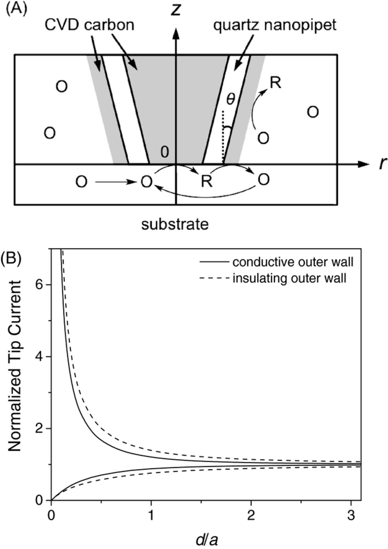
Figure 1. (A) Scheme of redox reactions at the tip and the conductive outer wall as defined in the cylindrical coordinate for simulation of SECM approach curves. (B) Approach curves simulated for a disk-shaped tip with a conductive and insulating outer wall (θ = 5° and RG = 1.4). The tip current was normalized against different iT,∞ values for a conductive and insulating outer wall (see Eq. 4).
The simulated approach curves at the conductive and insulating substrates clearly demonstrate that feedback responses significantly depend on the conductivity of the outer tip wall (Figure 1B). In these approach curves, the tip–substrate distance, d, is normalized against the inner tip radius, a, while the tip current is normalized against the tip current in the bulk solution, iT,∞. As expected, our simulation results demonstrate that iT,∞ also depends on the conductivity of the outer wall as given by
![Equation ([4])](https://content.cld.iop.org/journals/1945-7111/163/4/H3032/revision1/d0004.gif)
where x = 1.37 and 1.13 for the conductive and insulating outer wall with θ = 5° and RG = 1.4, respectively. A significantly larger x value for a conductive outer wall indicates that a significant fraction of the tip-generated species is electrolyzed at the wall to regenerate the original redox species for the tip reaction (Figure 1A). Subsequently, a lower positive feedback response is expected when a tip with a conductive outer wall approaches a conductive substrate, where a smaller fraction of the tip-generated species is available for the regeneration of the original redox species. Similarly, a less negative feedback effect is expected for a nanotip with a conductive outer wall, which regenerates the original species to enhance the tip current. Noticeably, the effect of a conductive outer wall on the tip current becomes smaller for a thicker quartz sheath.
Experimental
Chemicals and materials
Ru(NH3)6Cl3 was obtained from Strem Chemicals (Newburyport, MA). SiO2-coated silicon wafers were obtained from Graphene Laboratories (Calverton, NY). Silicon wafers coated with a 5.0 nm-thick titanium adhesion layer and then with a 100 nm-thick gold layer were obtained from Platypus Technologies (Madison, WI). All sample solutions were prepared by using ultrapure water with total organic carbon (TOC) of ≤1 ppb,35 which was obtained by passing the final product of the Milli-Q Advantage A10 system (EMD Millipore, Billerica, MA) through a specific activated-carbon filter (VOC Pak, EMD Millipore). The Milli-Q water purification system was equipped with a Q-Gard T1 pack and a Quantum TEX cartridge (EMD Millipore) in order to produce ultrapure water with 18.2 MΩ·cm and TOC of 3 ppb. The Milli-Q system was fed with purified tap water (15.0 MΩ·cm) as obtained by using the Elix 3 Advantage system (EMD Millipore).
Tip fabrication and characterization
A nanopipet was heat-pulled from a quartz capillary (1.0 mm outer diameter and 0.7 mm inner diameter, Sutter Instrument, Novato, CA) and filled with carbon by CVD to yield a slightly recessed tip.24 Specifically, a nanopipet with a tip diameter of 10–100 nm was pulled by using a program based on HEAT = 800, FIL = 4, VEL = 22, DEL = 128, PUL = 110 and HEAT = 830, FIL = 3, VEL = 17, DEL = 130, PUL = 255. A nanopipet was nearly completely filled with carbon deposited from methane in argon (1:1 ratio) for 1 hour at 900 °C. A copper nickel wire (0.13 mm diameter, Alfa Aesar, Ward Hill, PA) was used to establish a connection with a carbon nanotip for electrochemical measurements as well as its grounding to a sample stage in TEM, scanning electron microscopy (SEM), and FIB experiments and for protections from electrostatic damage. A recessed tip was milled by using an FIB instrument (SMI3050SE FIB-SEM, Seiko Instruments, Chiba, Japan)28,29 to yield a flat tip as confirmed by TEM (JEM-2100, JEOL USA, Peabody, MA).36 The beam of gallium ion (30 keV and 10 pA) was focused at a carbon nanotip for ∼3 second to mill the tip end, whereas the prior adjustment of the FIB condition took several minutes. A carbon nanotip was also characterized by SEM with the dual-beam FIB instrument before and after milling.
Electrochemical measurements
A homebuilt SECM instrument37 was used for electrochemical measurements with CVD carbon nanotips. A patch-clamp amplifier (Chem-Clamp, Dagan, Minneapolis, MN) was used as a two-electrode potentiostat to prevent the electrochemical damage of a nanotip.30 A Ag/AgCl wire was used as a counter/reference electrode. SiO2- and Au-coated silicon wafers were cleaned in piranha solution (a 1:3 mixture of 30% H2O2 and 95.0–98.0% H2SO4) for 30 minutes and in Milli-Q water for 15 minutes (3 times), and immediately immersed into the electrolyte solution contained in an SECM cell (Caution: piranha solution reacts violently with organics and should be handled with extreme care!). The electrolyte solution was prepared by dissolving Ru(NH3)6Cl3 in phosphate buffer solution (PBS) at pH 7.4 containing 0.137 M NaCl, 0.0027 M KCl, 0.01 M Na2HPO4, and 0.0018 M KH2PO4. The SECM cell was cleaned and sealed using a rubber cap and silicon gaskets in order to prevent the contamination of the electrolyte solution with airborne organic impurities.35 When a tip was attached to the SECM stage, the perpendicular alignment of the tip's axis with respect to the substrate surface was confirmed within ±0.5° by using a digital angle gauge.
Results and Discussion
TEM, SEM and FIB imaging
CVD carbon nanoelectrodes were characterized by TEM, SEM, and FIB imaging before and after FIB milling. We selected a CVD condition to obtain a recessed tip without the formation of a conductive carbon film on the outer tip wall.24 The high-resolution TEM image of an unmilled carbon nanotip confirmed the ∼70 nm-depth recession of CVD carbon from the ∼20 nm-radius orifice of the heat-pulled quartz pipet (Figure 2A). The hemispherical tip of CVD carbon had a base radius of ∼25 nm and was surrounded by a ∼10 nm-thick quartz wall, which corresponds to an RG value of ∼1.4 as expected from the corresponding RG value of quartz capillaries. A recessed carbon nanotip was milled by FIB and imaged by TEM to confirm that the tip was flat and completely filled with CVD carbon to yield an outer tip radius of ∼75 nm (Figure 2B). The excellent smoothness of a FIB-milled tip was achieved by employing a low current gallium ion (Ga+) beam (10 pA at 30 keV). Noticeably, TEM images showed that the edge of the milled tips was rounded, which is ascribed to the Gaussian broadening of the focused Ga+ beam.38
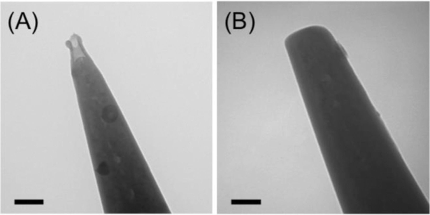
Figure 2. TEM images of carbon nanotips (A) before and (B) after FIB milling. Scale bar, 100 nm.
The dual-beam FIB/SEM instrument allowed us to visualize the tip of a carbon nanoelectrode by FIB and SEM imaging before and after milling. The resolution of an SEM image was high enough to ensure the intact tip end prior to milling (Figure 3A) when the tip was protected from electrostatic damage (see below). The tip end of an FIB-milled carbon nanotip was also clearly seen by SEM, which enabled us to estimate the outer radius of each milled tip. This information was useful for the analysis of electrochemical data, which depend not only on the radius of a carbon tip, a, but also on the outer radius of the quartz sheath, rg ( = ∼50 nm in Figure 3B). The outer radius of the smallest FIB-milled tip was practically limited to ∼50 nm by the resolution of FIB imaging, which was needed to locate the tip position prior to milling (Figure 3C). Accordingly, the Ga+ beam was focused slightly above the 50 nm-radius portion of the unmilled quartz nanopipet to yield a milled nanotip with an outer radius of ∼50 nm as checked by FIB and SEM imaging (Figures 3B and 3D, respectively). Noticeably, the blurriness of SEM and FIB images is due to the charging of the insulating quartz surface.
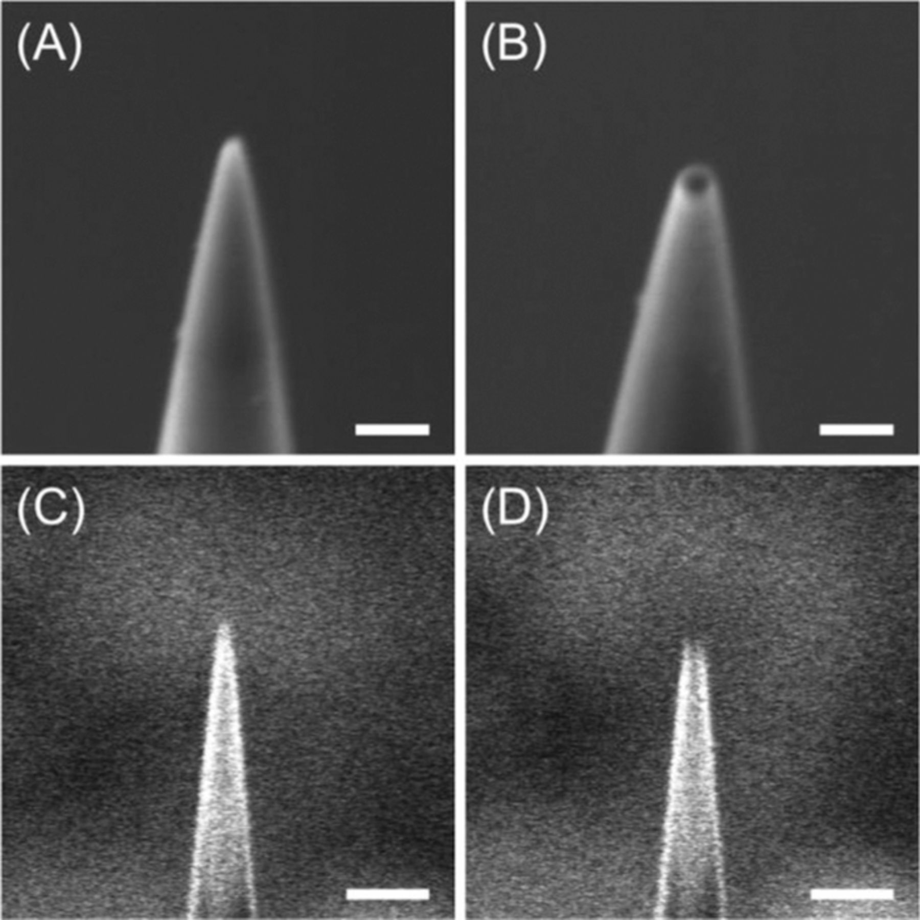
Figure 3. SEM images of (A) unmilled and (B) FIB-milled carbon nanotips and the corresponding FIB images in parts C and D, respectively. Scale bars: 200 nm in parts A and B, and 500 nm in parts C and D.
Voltammetric characterization
FIB-milled carbon nanoelectrodes were characterized by cyclic voltammetry (CV) to demonstrate their high electrochemical reactivity to the reduction of Ru(NH3)63+, which yielded nearly reversible CVs with well-defined limiting currents, iT,∞. The inner radius of a nanotip (a = 49 and 29 nm in Figures 4A and 4B, respectively) was determined from the limiting current by using Eq. 4 with D = 6.7 × 10⁻⁶ cm2/s for Ru(NH3)63+.39 In addition, this analysis employed a simulated x value of 1.13 in Eq. 4 for an insulating outer wall with RG and θ values as determined by TEM. Thus, an inner tip radius determined voltammetrically gave an outer radius that is consistent with the outer radius estimated by SEM. Noticeably, we employed SECM to confirm the size and geometry of an FIB-milled carbon nanotip as well as a lack of a conductive carbon film on the outer wall (see below).
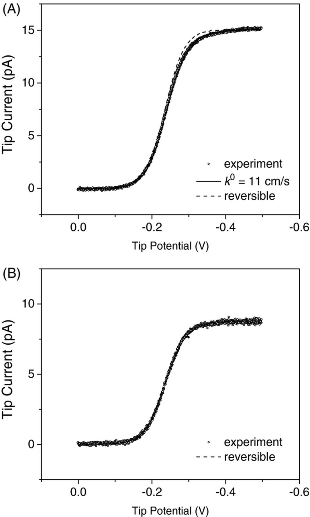
Figure 4. CVs (circles) of 1 mM Ru(NH3)6Cl3 in PBS at (A) 49 and (B) 29 nm-radius tips of FIB-milled CVD carbon nanoelectrodes. Solid and dashed lines represent simulated CVs.
Nearly reversible CVs of Ru(NH3)63+ were analyzed to yield extremely high standard electron-transfer rate constants, k0, of ≥10 cm/s by using four carbon nanoelectrodes with tip radii of <50 nm. For instance, the slightly quasi-reversible CV of Ru(NH3)63+ at the 49 nm-radius carbon electrode fitted well with a simulated CV with a k0 value of 11 cm/s (i.e., k0a/D = 8) and a transfer coefficient, α, of 0.5. On the other hand, the reversible CV of Ru(NH3)63+ at the 29 nm-radius carbon electrode yielded an even larger k0 value of ≥23 cm/s (i.e., k0a/D ≥ 10). These k0 values for Ru(NH3)63+ at FIB-milled carbon nanoelectrodes are close to k0 values of 17 cm/s at platinum nanoelectrodes,40 13 cm/s at gold nanoelectrodes,41 and 4 cm/s at individual single-walled carbon nanotubes.42 Similar k0 values for Ru(NH3)63+ among different electrode materials have been considered as evidence of adiabatic electron-transfer reactions.43,44 We, however, emphasize that nanoelectrodes can be readily contaminated with adventitious impurities from ultrapure water45 and ambient air, which may apparently limit k0 values to the similar values.35 Moreover, the electron-transfer kinetics of Ru(NH3)63+ at FIB-milled carbon nanotips may be affected by the implantation of gallium ion on the carbon surface.38 In addition to these uncontrollable contaminants, the amorphous form of CVD carbon might have caused differences among the k0 values obtained by using different FIB-milled carbon nanoelectrodes (Figure 4).
Approach curves at an insulating substrate
The well-defined geometry of FIB-milled carbon nanotips was confirmed by SECM approach curves at insulating substrates, where negative feedback responses are sensitive to the thickness of the insulating sheath46,47 as well as the conductivity of the outer wall (see the Theory section). Experimentally, Ru(NH3)63+ was reduced at a carbon nanotip at a diffusion-limited rate while the tip approached a SiO2-coated silicon wafer as a flat insulating substrate. Figure 5A shows the resultant approach curve as obtained using a relatively large carbon nanoelectrode (a = 119 nm). The normalized experimental approach curve fitted well with a simulated approach curve for a tip with an insulating outer wall, but not with a curve for a tip with a conductive outer wall. The good fit was obtained by using an RG value of 1.4 as estimated by TEM. The theoretical analysis also yielded a very short distance of the closest approach, dc, (i.e., the closest tip–substrate distance where the experimental curve fits with the theoretical curve) to be 8 nm, which confirms the flat tip end (Figure 2B). By contrast, much larger dc values of 50–150 nm were reported for pyrolytic carbon nanoelectrodes with a similar size (a = 120–150 nm and RG = 1.5) at insulating substrates.14,15
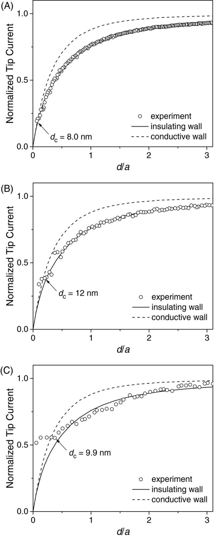
Figure 5. Approach curves of SiO2-coated silicon wafers as obtained by using FIB-milled carbon nanotips with a = (A) 119, (B) 44, and 27 nm in PBS of 1 mM Ru(NH3)6Cl3. Solid and dashed lines represent simulated curves.
Remarkably, good fits between experimental and simulated approach curves at an insulating substrate were obtained for FIB-milled nanoelectrodes with carbon radii of <50 nm. Figures 5B and 5C show approach curves for FIB-milled carbon nanotips with a = 44 and 27 nm, respectively, where good fits were obtained at short distances of ∼10 nm for the closest tip–substrate approach. These approach curves are strikingly different from those obtained previously with sub-100 nm-diameter carbon electrodes.14–17 For instance a radius of 6 nm was determined for a pyrolytic carbon nanoelectrode from a approach curve at an insulating substrate that showed a decrease of only 15% in the tip current and significantly deviated from SECM theory for a disk tip,15 thereby suggesting that the extremely small value of the tip radius may not be reliable. Noticeably, closest tip–substrate distances in this study were consistently ∼10 nm for carbon nanotips with different radii (Figure 5), whereas the tip end was very flat (see Figure 2B). We speculate that the closest tip–substrate approach was limited by the contamination of tips, e.g., with aerosol nanoparticles during their storage in ambient air. Unfortunately, the cleaning of a carbon nanotip in piranha solution or by a UV cleaner damaged the tip end.
Approach curves at a conductive substrate
We employed FIB-milled carbon nanotips to study approach curves at gold-coated silicon wafers. Since the surface area of the unbiased gold film was much larger than that of a carbon nanotip, we expected that a positive feedback response would be limited by the diffusion of Ru(NH3)63+ between the tip and the substrate.48,49 A feedback response, however, was much lower than the diffusion-limited response when 5.0 mM Ru(NH3)6Cl3 was employed (Figure 6A). The tip current was enhanced only by a factor of ∼1.6 before the 134 nm-radius carbon tip nearly contacted the gold substrate to give much higher currents. Apparently, this approach curve agreed with a theoretical approach curve50 limited by the irreversible oxidation of Ru(NH3)62+ at the gold surface to yield an electron-transfer rate constant, ket, of 1.1 cm/s. The tip current, however, was limited not by the kinetics of Ru(NH3)62+ oxidation, but by the subsequent transport of electrons through the thin gold film, because a higher positive feedback response was obtained as the concentration of Ru(NH3)6Cl3 was lowered.51 Specifically, approach curves with 1 and 0.2 mM Ru(NH3)6Cl3 (Figures 6B and 6C, respectively) yielded the highest normalized tip currents of ∼3.5 and ∼6.0, respectively. The latter approach curve fitted well with the diffusion-limited approach curve at a conductive substrate to yield a short distance of 20 nm for the closet approach of the 139 nm-radius tip to the gold surface. Importantly, the limited conductivity of the gold films was manifested owing to extremely high mass-transport conditions under carbon nanotips. By contrast, the film conductivity was high enough to obtain high positive feedback responses by using 1 μm-diameter Pt tips.35 In addition, the CVs of Ru(NH3)6Cl3 at a gold-coated silicon wafer gave a wider peak separation at a higher concentration of the redox species owing to an uncompensated resistance through a gold film, which was estimated to be 1.8 × 10² Ω according to the method proposed by McCreery and co-workers.52
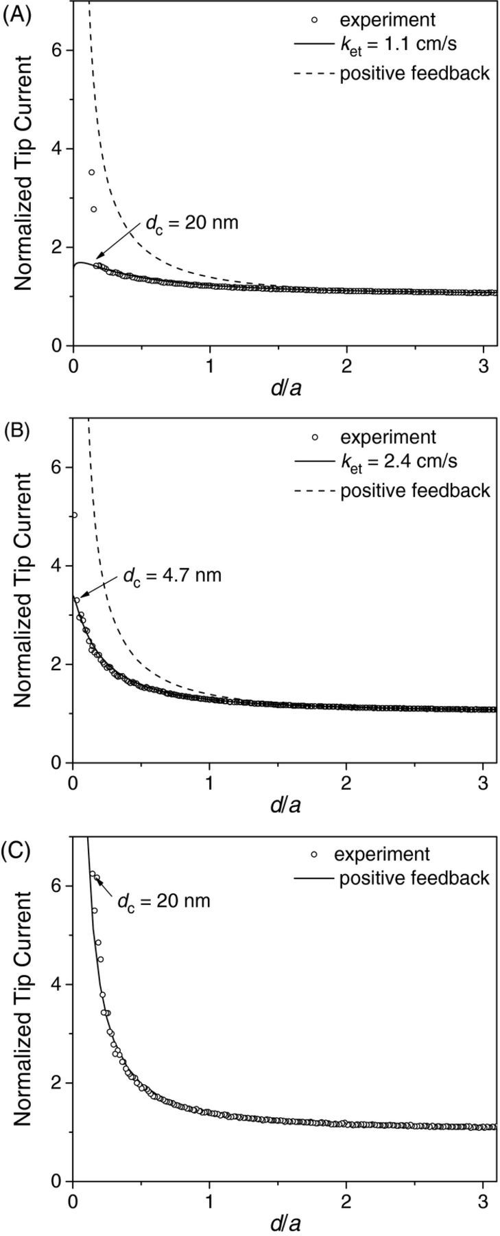
Figure 6. Approach curves at gold-coated silicon wafers as obtained with (A) 5.0, (B) 1.0, and (C) 0.2 mM Ru(NH3)6Cl3 in PBS by using FIB-milled carbon nanotips with a = 134, 123, and 139 nm, respectively. Solid and dashed lines represent theoretical curves from Ref. 50.
It was reported previously that a pyrolytic carbon nanoelectrode gave a positive feedback response that was much lower than a diffusion-limited response as expected for a platinum substrate electrode.14 The low feedback response was ascribed to a kinetic effect and was fitted with a kinetically limited theoretical response. The rather poor fit yielded an unrealistically low ket value of 0.8 cm/s for the ferrocenemethanol couple in comparison with a k0 value of 6.8 cm/s for this couple at platinum nanoelectrodes.40 Alternatively, the low positive feedback response can be ascribed to the limited substrate conductivity51 or the tip recession.53
Electrostatic tip damage
To enable quantitative nanoelectrochemical measurements discussed above, one has to avoid the nanoscale damage of carbon nanotips caused by electrostatic discharge (ESD).30 Specifically, the tip of a carbon nanoelectrode was maintained intact without ESD damage when an operator employed ESD protections30 and handled the nanoelectrode under a high humidity of ∼50%31 in a plastic box equipped with a humidifier. In addition, we had to ground the lead wire of a carbon nanoelectrode when its tip was inspected by optical microscopy, where a sufficiently high humidity was not achievable. In fact, we found that ESD damage was caused unknowingly when the ungrounded lead wire of a carbon nanoelectrode contacted an insulated stage of the optical microscope under low humidity (<30%). ESD-damaged carbon nanotips had nanometer-sized pinholes when they were imaged by SEM prior to FIB milling (Figure 7A). In addition to pinholes, cracks were observed in FIB-milled carbon nanotips by SEM (Figure 7B) after they were used for CV measurements in the bulk solution. ESD damage was noticeable during the CV measurements, where the tip current was much higher than expected from the tip size owing to the diffusional access of Ru(NH3)63+ to the carbon surface through pinholes and cracks.
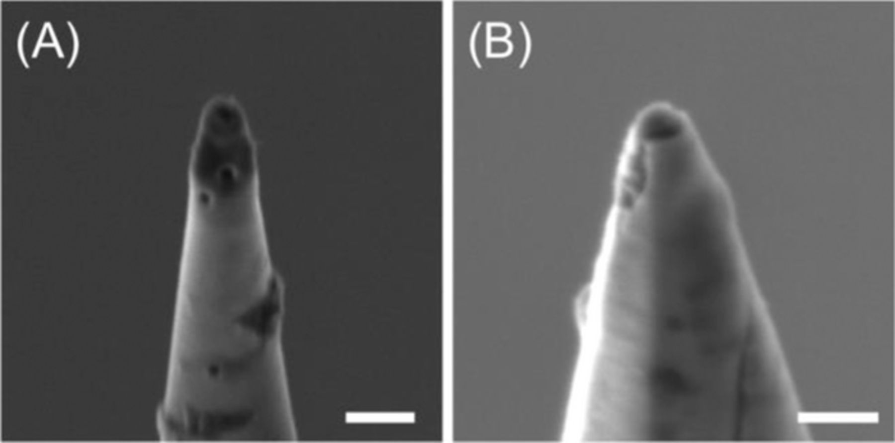
Figure 7. SEM images of (A) unmilled and (B) FIB-milled carbon nanotips with ESD damage. The latter tip was used for CV measurements in the bulk solution before SEM imaging. Scale bars: (A) 500 nm and (B) 200 nm.
Conclusions
In this work, we demonstrated that FIB-milled CVD carbon nanoelectrodes are useful as SECM nanotips with high electrochemical reactivity and well-controlled size and geometry. Flat carbon nanotips with the smallest inner and outer radii of ∼27 and ∼38 nm, respectively, were characterized by TEM and SEM and applied to SECM approach curve measurements. A lack of a conductive carbon layer on the outer tip wall was confirmed by approach curves at insulating substrates. FIB-milled carbon nanoelectrodes also revealed the limited conductivity of ∼100 nm-thick gold films under extremely high mass-transfer conditions, where the carbon nanotips were sufficiently conductive and reactive. In addition, we found that nanopipet-supported CVD carbon tips can be damaged by ESD, while ESD damage was previously reported only for glass-sealed Pt nanoelectrodes30,31 and not for nanopipet-supported pyrolytic carbon tips.17 Damage-free carbon nanoelectrodes will enable reliable and quantitative nanoelectrochemical measurements including high-resolution SECM imaging54 and SECM-based nanogap voltammetry.28,35
Acknowledgments
This work was supported by the National Science Foundation (CHE-1213452 for SA and CHE-1300158 for MM), the National Institutes of Health (R01 GM112656 for SA), and the Air Force Office of Scientific Research (MURI FA9550-14-1-0003 for MM).