Article

Application of the Composite Hardness Models in the Analysis of Mechanical Characteristics of Electrolytically Deposited Copper Coatings: The Effect of the Type of Substrate

by
Ivana O. Mladenović
1,*,
Nebojša D. Nikolić
1,
Jelena S. Lamovec
2,
Dana Vasiljević-Radović
1 and
Vesna Radojević
3
1
Institute of Chemistry, Technology and Metallurgy, University of Belgrade, Njegoševa 12, 11 000 Belgrade, Serbia
2
University of Criminal Investigation and Police Studies, Cara Dušana 196, Zemun, 11 000 Belgrade, Serbia
3
Faculty of Technology and Metallurgy, University of Belgrade, Karnegijeva 4, 11 000 Belgrade, Serbia
*
Author to whom correspondence should be addressed.
Metals 2021, 11(1), 111; https://doi.org/10.3390/met11010111
Submission received: 15 December 2020 / Revised: 2 January 2021 / Accepted: 4 January 2021 / Published: 8 January 2021

Abstract

:
The mechanical characteristics of electrochemically deposited copper coatings have been examined by application of two hardness composite models: the Chicot-Lesage (C-L) and the Cheng-Gao (C-G) models. The 10, 20, 40 and 60 µm thick fine-grained Cu coatings were electrodeposited on the brass by the regime of pulsating current (PC) at an average current density of 50 mA cm−2, and were characterized by scanning electron (SEM), atomic force (AFM) and optical (OM) microscopes. By application of the C-L model we determined a limiting relative indentation depth (RID) value that separates the area of the coating hardness from that with a strong effect of the substrate on the measured composite hardness. The coating hardness values in the 0.9418–1.1399 GPa range, obtained by the C-G model, confirmed the assumption that the Cu coatings on the brass belongs to the “soft film on hard substrate” composite hardness system. The obtained stress exponents in the 4.35–7.69 range at an applied load of 0.49 N indicated that the dominant creep mechanism is the dislocation creep and the dislocation climb. The obtained mechanical characteristics were compared with those recently obtained on the Si(111) substrate, and the effects of substrate characteristics such as hardness and roughness on the mechanical characteristics of the electrodeposited Cu coatings were discussed and explained.

1. Introduction

Copper electrodeposition is of high significance, attracting much attention in both the scientific and technological sectors, with numerous applications in many industrial branches. The main industrial branches using the copper coatings are the electrical, electronic, automotive, defense industries, etc. [1]. Application of this metal is based on its excellent electrical and thermal conductivity, as well as its corrosion-resistant characteristics, enabling the application of electrolytically formed Cu thin films and coatings for the interconnection of printed circuit boards (PCBs) and ultra large scale integration (ULSI), wiring so-called damascene process, etc. [2,3]. The electrolytically synthesized Cu coatings possess a good adhesiveness, making Cu a highly effective undercoat before applying other coatings such as tin or nickel. Sometimes a harder surface may be required, and then copper electroplating can be used to increase surface strength [1].
The good mechanical characteristics of the Cu coatings attained by application of the electrodeposition technique determine the advantage of this technique over the other methods of synthesis, such as physical vapor deposition (PVD) [4], chemical vapor deposition (CVD) [5], and magnetron sputtering [6]. Electrodeposition is a low-equipment- and -product-cost, environmentally friendly, time-saving and facile technique [7]. This method also offers a possibility of the easy control of the thickness of coatings, as well as the obtaining of coatings of desired features by a suitable selection of parameters and regimes of electrodeposition [8]. The parameters of electrodeposition determine the morphological and structural characteristics, and thus, the mechanical characteristics of metal coatings are the type and composition of electrolyte, the addition of additives in the electrolyte, the type of substrate (cathode), mixing of electrolyte, temperature, etc.
In the constant galvanostatic (DC) regime, the compact adherent coatings of copper with fine-grained structure are mainly obtained in the presence of various additives. The acid sulfate electrolytes consisting of copper sulfate and sulfuric acid are the most often-used electrolytes for Cu electrodeposition. Thiourea is a traditionally used additive for obtaining fine-grained deposits of Cu [9,10]. In the last two decades, the combination of additives based on chlorides and PEG poly(ethylene glycol) with an addition of bis-3-sulfopropyl-disulfide (SPS) [11,12,13] or 3-mercapto-2-propanesulphonic acid (MPSA) [14,15,16] also found wide application. The concentration of the leveling and brightening addition agents is incomparable with the concentration of the basic components of electrolyte, which causes their fast consumption and the need for the permanent control and correction of the composition of the electrolyte. In order to avoid the use of additives, various periodically changing regimes of electrodeposition, such as pulsating and reversing current regimes, were proposed for obtaining compact uniform coatings [8,17,18,19,20]. The lower-porosity and fine-grained structure of deposits are achieved by the simple regulation of parameters constructing these regimes. The mixing of electrolytes also contributes to an improvement of the quality of coatings produced by various electrodeposition techniques [18,21,22,23].
All the above-mentioned parameters and regimes of the electrodeposition affecting the quality, i.e., morphological and structural characteristics, of the coatings simultaneously determine their mechanical characteristics. The hardness of the coatings is one of the most important mechanical characteristics, and it can be determined by directly using low indentation loads, or indirectly by application of the composite hardness models. Both these ways have advantages and disadvantages, and a balance between them is necessary. The direct approach is suitable for thick coatings excluding any contribution of a substrate to measure the hardness value, but the limit of this approach is the insufficient precision of a diagonal size measurement at the low indentation load. The indirect approach takes into account the contribution of substrate hardness to measure the hardness value [24,25]. The main disadvantage of the application of these models is the absence of their universal character, with numerous limitations to the calculation of true (or absolute) hardness from the measured composite hardness.
Various composite hardness models, such as Burnett-Rickerby (B-R) [26,27], Chicot-Lesage (C-L) [28,29,30,31], Chen-Gao (C-G) [32,33,34,35] and Korsunsky (K-model) [36,37,38,39], are proposed for the determination of the true hardness of metal coatings. The choice of composite hardness the model depends on the coating/substrate hardness ratios, and some of them are applied for a “hard coating-soft substrate“ system, such as the Korsunsky model, while some other models are suitable for the analysis of “soft film-hard substrate“ systems, such as the Chen-Gao [32,33,34,35] and the Chicot-Lesage [28,29,30,31] composite hardness models. For the same metal coating, the choice of the composite hardness model is determined by the type of used substrate. The following substrates are the often applied in the Cu electroplating processes: silicon [20,25,35,38], nickel coatings [14,21], copper [9,10,19,38], polyimide [5], graphite [23] or brass [21].
The other very important mechanical characteristic of coatings is their creep resistance. The creep resistance of the coatings gives very valuable information related to the time-dependent flow of materials [40], i.e., to an evaluation of their reliability. It is necessary to stress that aside from the data obtained for the Cu coatings electrodeposited on the Si(111) substrate by the PC regime [25], other data dealing with the analysis of this mechanical characteristic are not found in the literature for the copper coatings.
Regarding the role of the substrate in relation to the mechanical characteristics of metal coatings, the aim of this study is to examine the contribution of brass as the type of cathode on the hardness and creep resistance of the Cu coatings electrodeposited by the PC regime. In order to better perceive the role of the substrate, the obtained results will be discussed and compared with those recently observed for the Cu coatings electrodeposited under the same conditions on the Si(111) substrate belonging to the group of very hard substrates. Special attention will be devoted to a determination of the precise boundary that separates the area with absolute coating hardness from the area where the contribution of substrate hardness must be taken into account. In spite of numerous investigations related to the hardness analysis of electrolytically deposited coatings, the results dealing with a definition of the limiting value separating these two areas are not reported in the literature, and for that reason, it will be achieved in this study by application of the C-L model for the first time.

2. Materials and Methods

2.1. Preparation of Samples by Electrodeposition Process for Mechanical Characterization

The electrodeposition of copper was performed from 240 g/L CuSO4⋅5 H2O in 60 g/L H2SO4 at room temperature in an open square-shaped electrochemical cell. For the electrodeposition process, the regime of pulsating current (PC) with the following parameters was applied: jA = 100 mA cm−2, tc = 5 ms and tp = 5 ms. In the PC regime, the electrodeposition process occurs at the average current density (jav, in mA cm−2) defined by Equation (1) [8]:
j a v = j A t c t c + t p
where jA (in mA cm−2) is the current density amplitude, tc (in ms) is the deposition pulse, and tp (in ms) is the pause duration. With these parameters of the PC regime, jav was 50 mA cm−2. The thicknesses of the Cu coatings were 10, 20, 40 and 60 μm. Brass (2601/2 hard, ASTM B36, K&S Engineering) with a 1.0 × 1.0 cm2 surface area was used as a cathode, and copper plate with a 8.0 × 5.0 cm2 surface area was used as an anode. The cathode was situated in the middle of the cell between two parallel Cu plates. The distance between anode and cathode was 2.0 cm. Preparation of the brass electrodes for electrodeposition was performed as follows: The brass cathode was ground by # 800, # 1000 and # 1200 SiC sandpapers and rinsed in water. Then, it was degreased at a temperature of 70 °C, followed by acid etching (20% H2SO4) at 50 °C. After each phase, the cathodes were rinsed with distilled water. For a preparation of the electrolyte, doubly distilled water and analytical-grade reagents were used.

2.2. Characterization of the Produced Cu Coatings

The following techniques were used for characterization:
(a)
Scanning electron microscope (SEM), model JEOL JSM-6610LV (JEOL Ltd., Tokyo, Japan)—morphological analysis;
(b)
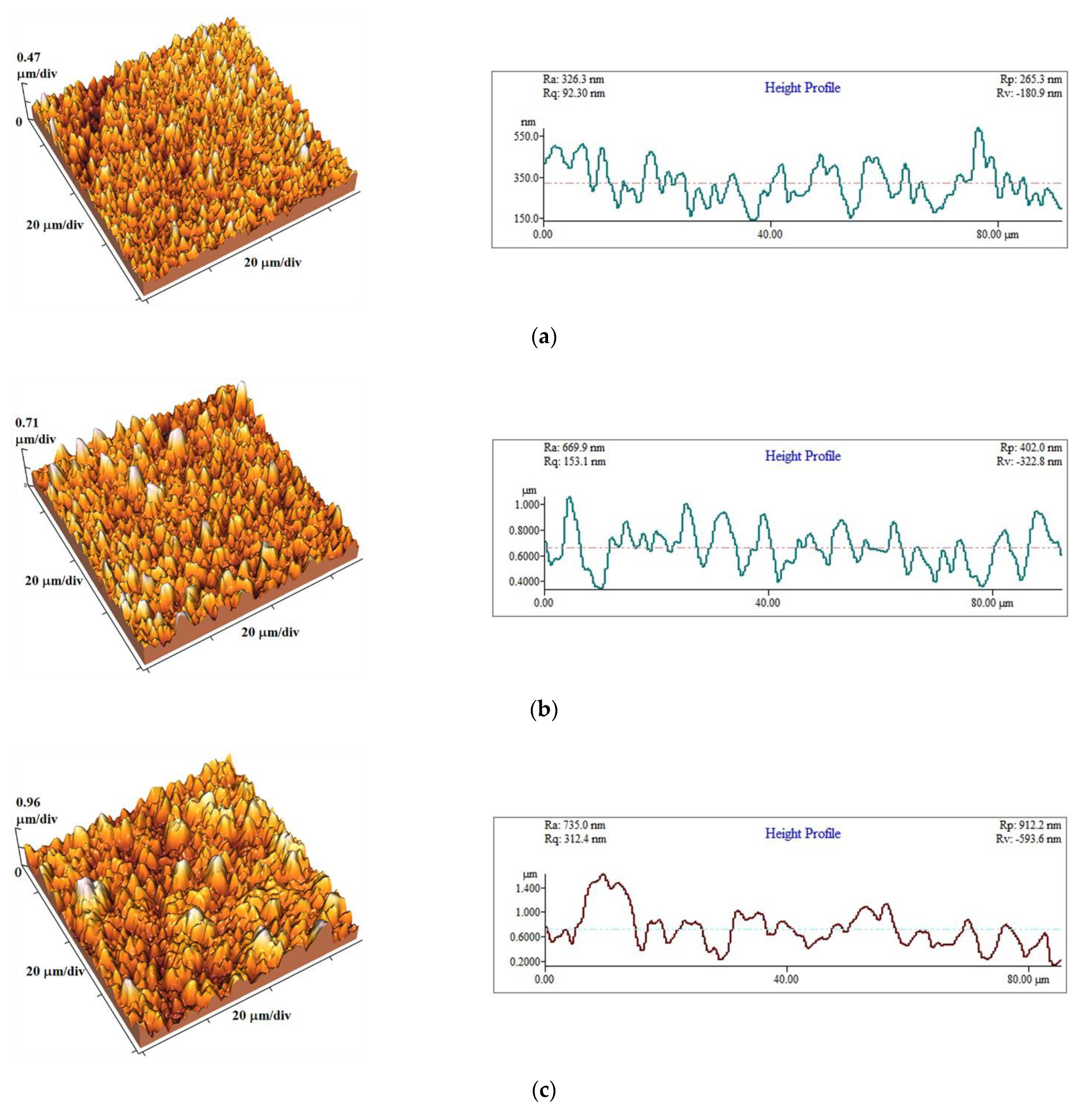
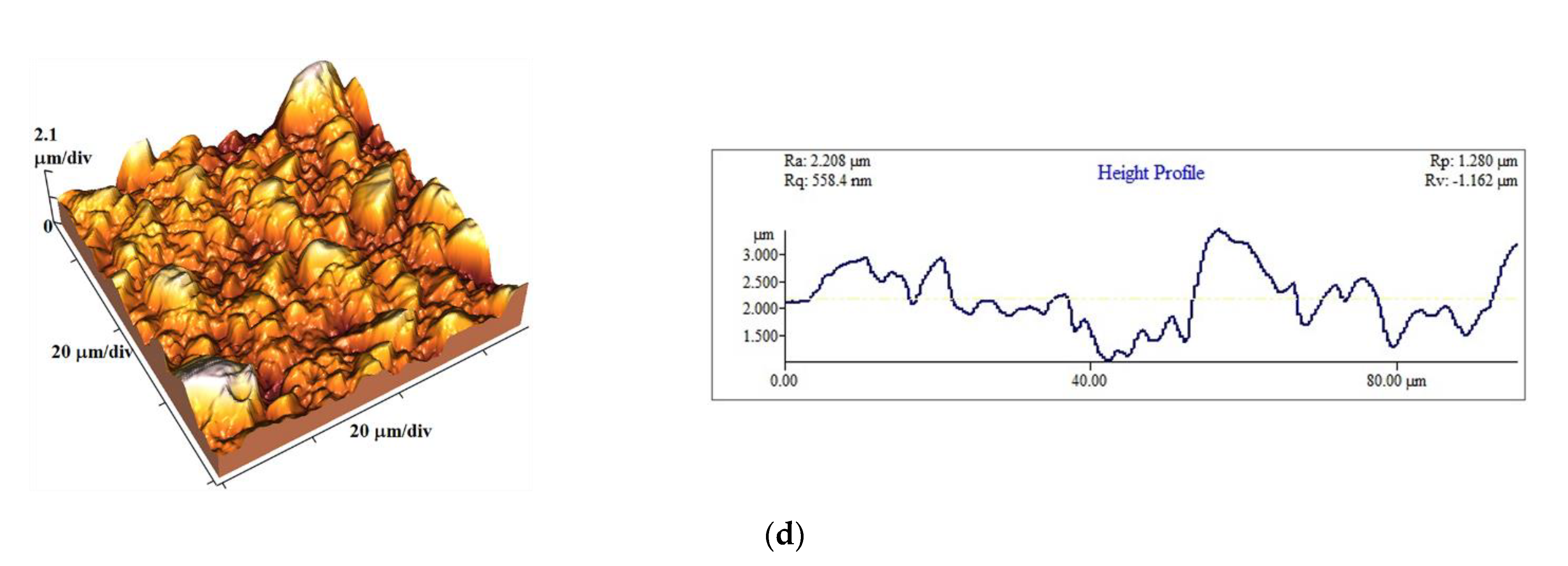
Atomic force microscope (AFM), model Auto Probe CP Research. TM Microscopes, Veeco Instruments, Santa Barbara, CA, USA—topographical analysis of the coatings. The values of the arithmetic average of the absolute (Ra) roughness parameters were measured from the mean image data plane, using software SPLab (SPMLab NT Ver. 6.0.2., Veeco Instruments, Santa Barbara, CA, USA);
(c)
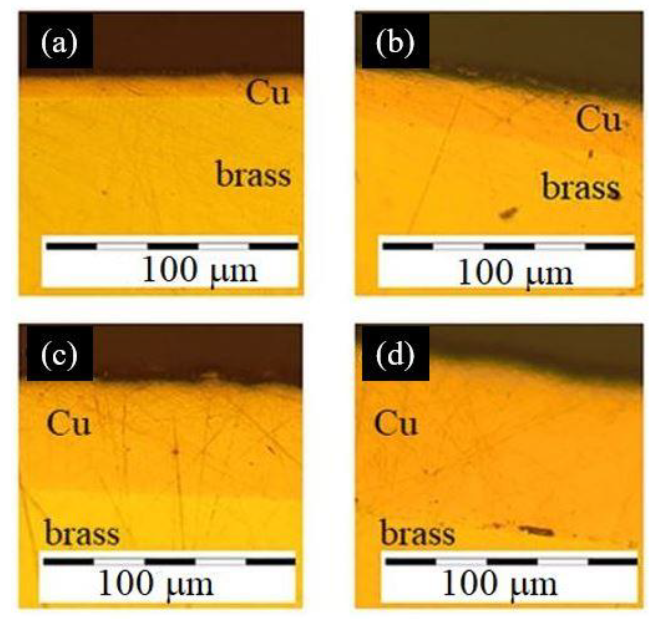
Optical microscope (OM), model Olympus CX41 connected to the computer—analysis of the internal structure (cross section analysis). The Cu coatings were immersed in self-curing acrylate (Veracril® New Stetic S. A., Antioquia, Colombia) using a mold. Three parts of self-cure polymer Veracril® and one part of self-cure monomer Veracril® were used for the mixture. The self-polymerization time at room temperature was 20 min. After polymerization, the samples were removed from the Teflon mold and mechanically polished by SiC sandpapers # 2000 and with Al2O3 powder emulsion with different grain sizes (1 and 0.3 μm). After rinsing in water and drying in nitrogen flow, the cross section was observed on an optical microscope and the coating thicknesses were measured.

2.3. Examination of the Mechanical Characteristics of the Cu Coatings

The mechanical characteristics of the Cu coatings were examined by use of a Vickers microhardness tester “Leitz Kleinert Prufer DURIMET I” (Leitz, Oberkochen, Germany). The number of applied loads and the dwell time depended on the type of analyzed mechanical characteristic. For the analysis of the hardness of the coatings, applied loads (P) in the 0.049–2.94 N range and a constant dwell time of 25 s were applied. The indentation creep characteristics of the Cu coatings were analyzed, varying the dwell time in the 15–65 s range with applied loads of 0.49 and 1.96 N.

3. Results

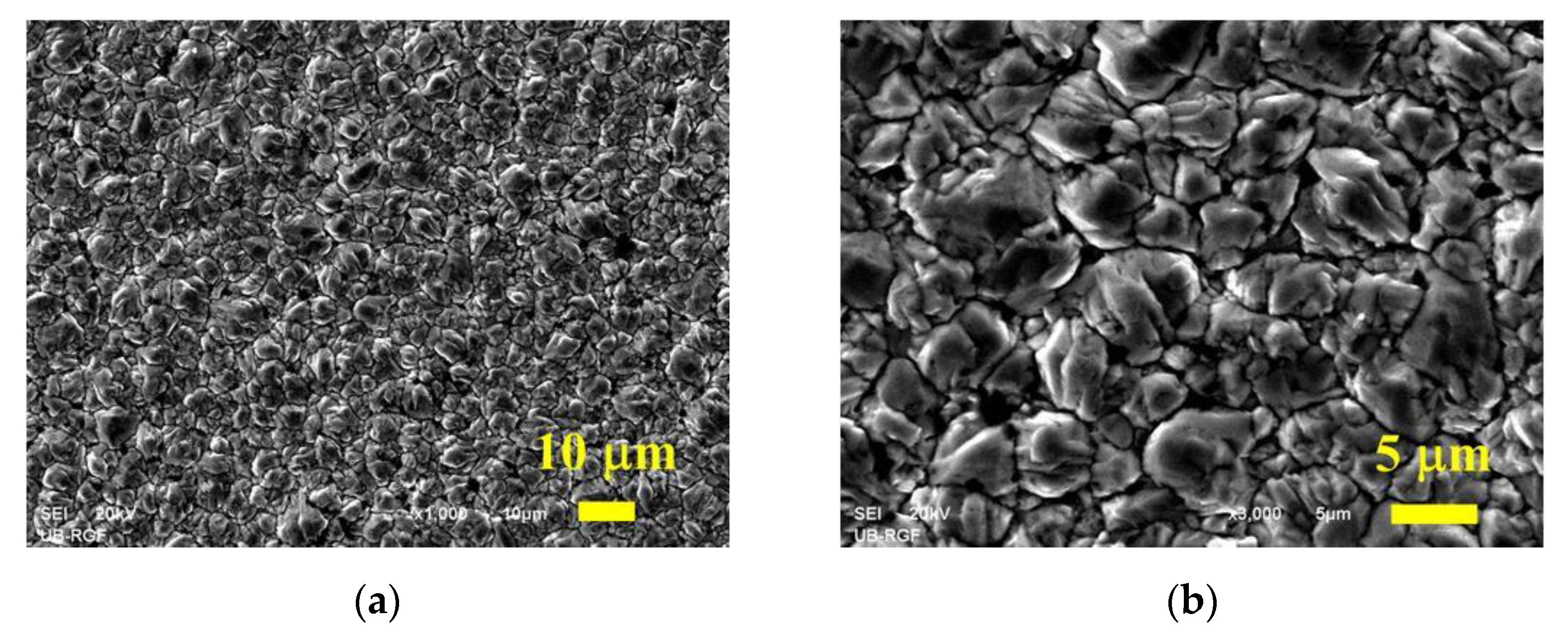
3.1. Characterization of the Copper Coatings Obtained by the PC Regime

The fine-grained copper coatings were formed by a square-wave pulsating current (PC) regime at a jav of 50 mA cm−2 (ν = 100 Hz), which was attained by application of the following parameters of this regime: tc = 5 ms, tp = 5 ms and jA = 100 mA cm−2 (Figure 1). With an overpotential amplitude response in the 290–350 mV range, the formation of this structure corresponds to the very beginning of the mixed activation–diffusion control, which represents the optimum for the formation of compact and uniform coatings [8,20].
Figure 2 shows 70 × 70 μm2 surface areas and the corresponding line section analyses of the Cu coatings with thicknesses of 10, 20, 40 and 60 μm obtained by applying the above-mentioned PC regime. The values of the arithmetic average of the absolute (Ra) roughness determined by the accompanied software are given in Table 1. The data were presented as the mean ± standard deviation for 12 measuring points. The increase in roughness of the coatings with increasing the thickness is clearly visible from both Figure 2 and Table 1, and this increase in roughness was about seven times.
A cross section analysis of the same Cu coatings is presented in Figure 3, from which the uniform and compact structure of the coatings of the projected thickness can be seen.

3.2. Analysis of the Mechanical Characteristics of the Cu Coatings

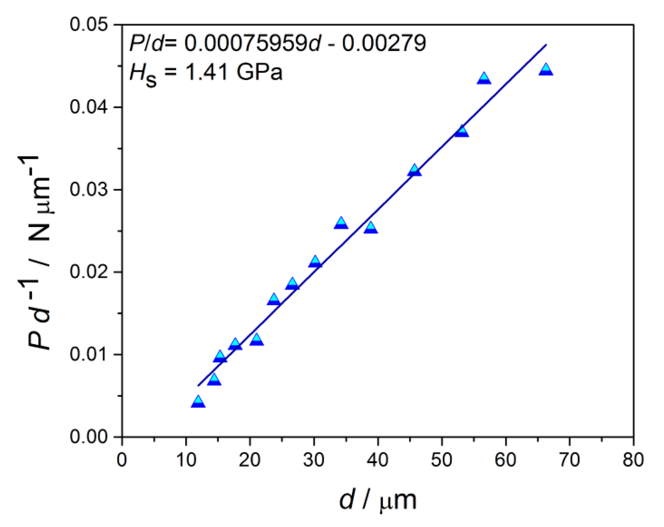
3.2.1. Determination of Absolute Hardness of Substrate (Brass)

In the application of various composite hardness models, the first step is a determination of the absolute (or true) hardness of a substrate. The composite hardness (Hc, in Pa) depends on the applied load (P, in N) and the measured diagonal size (d, in m) according to Equation (2) [20]:
H c = 1.8544 P d 2
The Vicker’s test is normalized by ASTM E384 and ISO 6507 standards [41,42], where P is measured in kgf and d in mm. If the applied load is expressed in N, then Equation (2) should be divided by 9.8065.
The model named PSR (proportional specimen resistance) is widely used for the determination of the absolute hardness of the substrate [43]. According to this model, the applied load and the measured diagonal size are related by Equation (3):
P = a 1 d + P c d 0 2 d 2
where Pc (in N) is the critical applied load above which microhardness becomes load-independent and d0 (in m) is the corresponding diagonal length of the indents. Figure 4 shows the dependence of P/d (in N∙μm−1) on d (in μm), from which slope an absolute hardness of the brass B36 substrate (Hs) of 1.41 GPa was calculated.

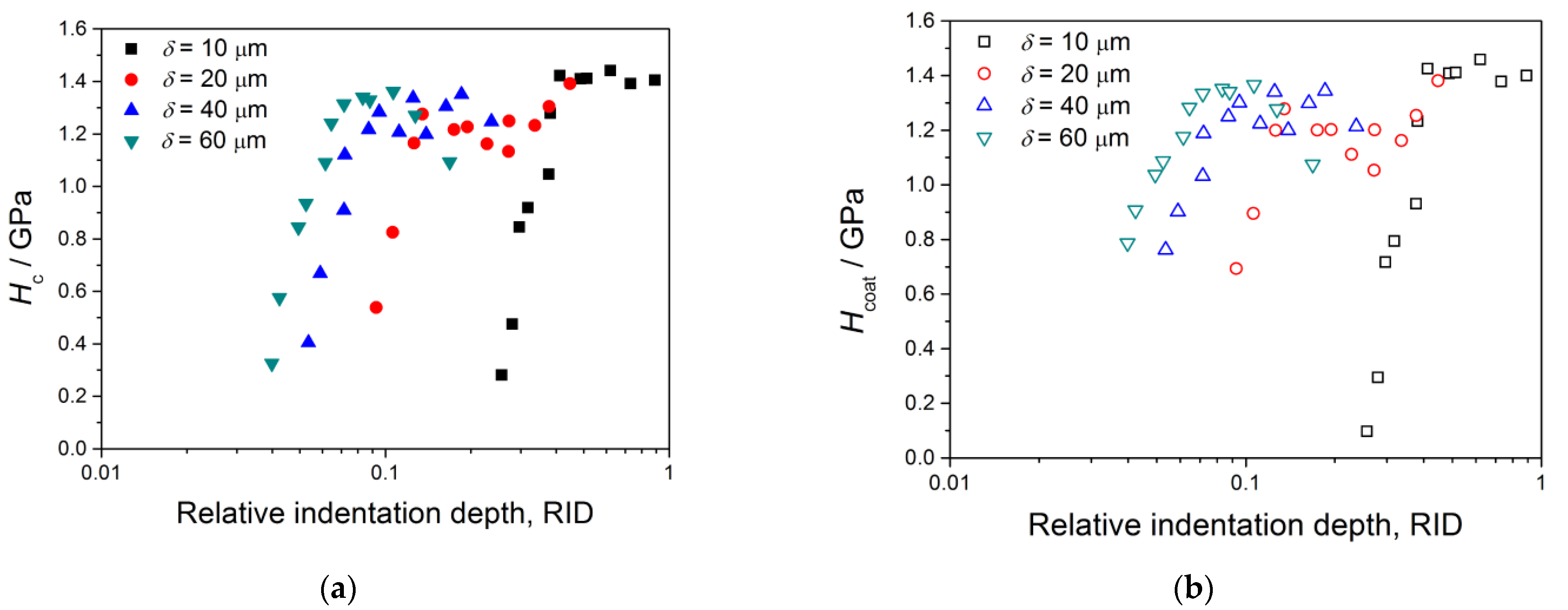
3.2.2. Hardness Analysis of Copper Coatings Electrodeposited on the Brass

The dependencies of the composite hardness, Hc, on the relative indentation depth (RID) for the Cu coatings thicknesses of 10, 20, 40 and 60 μm are shown in Figure 5a. The RID is defined as the ratio between indentation depth, h, and the thickness of the coating, δ (RID = h/δ), and RID values between 0.01 and 0.1 indicate the dominant effect of the hardness of the coating on the composite hardness [20,21,25,36,37,38,44]. For RID values between 0.1 and 1, both the substrate and the coating contribute to the composite value, and finally, RID values larger than 1 indicate the dominant effect of the substrate hardness on the composite hardness. The indentation depth is related with a measured diagonal size as h = d/7 [20,44].
For the coatings of 10 and 20 μm thicknesses, the RID values were between 0.1 and 1, indicating the contribution of both the brass and the electrodeposited Cu to the composite hardness. With increasing the coating thickness, the contribution of the coating hardness to the composite hardness (RID < 0.1) was increased, which can be seen from Figure 5a. Simultaneously, the highest value of composite hardness was shown by the 10 μm thick Cu coating.
Figure 5b shows the dependencies of the coating hardness (Hcoat) on the RID calculated according to the Chicot–Lesage (C-L) model. A similar shape of the dependencies to those obtained for the composite hardness on the RID was observed. A detailed presentation of the C-L model has been already given in Ref. [20].
An additional analysis was made with the aim of establishing a precise boundary of applicability of the C-L model, i.e., to establish a boundary whereat begins a strong contribution of the substrate to the composite hardness. For that purpose, the dependencies of the (δ/d)m on the RID for the Cu coatings of thicknesses of 10, 20, 40 and 60 µm were measured and are shown in Figure 6. The exponent m represents the composite Meyer′s index for a composite system, and it is calculated by the linear regression performed on all experimental points for the examined coating–substrate system [30,38,45,46]. The values of exponent m with R-squared values on ln(P)-ln(d) charts, obtained for the coatings of various thicknesses and 12 applied load points, are given in Table 2.
Taking a value of δ/d of 1 as a limit up to which the C-L model is applicable [28,29,30,31], the RID value of 0.14 was obtained (Figure 6). For the RID > 0.14, it is necessary to apply the composite hardness model in order to evaluate the coating hardness from the measured composite hardness, because the substrate hardness strongly affects the composite hardness value. For an RID < 0.14, the composite hardness corresponds to the coating hardness. The limitation of the application of the C-L model for the RID < 0.14 is confirmed by the fact that for the RID values smaller than this value the coating hardness becomes larger than the composite hardness, and this difference increases with a decreasing RID value (Figure 5).
To determine the true coating hardness values, another composite hardness model was applied. The shapes of the dependencies of the Hc on the RID shown in Figure 5a, as well as the value of the brass hardness of 1.41 GPa, indicate that the coatings of copper on brass belong to the “soft film on hard substrate” type of composite hardness system. For this reason, the Cheng-Gao (C-G) model [32,33,34,35] was used for a determination of the true hardness of the coating from the measured composite hardness. The C-G model has been developed for this type of composite system [33,35], and it is successfully implemented in a determination of the hardness of the copper coatings obtained by electrodeposition by the PC regime on a very hard Si(111) substrate [25]. According to the C-G model, a correlation between the composite hardness and the indentation depth is given by Equation (4) [33]:
H c = A + B 1 h + C 1 h n + 1
where, as already mentioned, Hc (in Pa) is the composite hardness, h (in m) is indentation depth, A, B and C are fitting parameters used for the calculation of the absolute or true coating hardness, and n is the power index. For the “soft film on hard substrate” composite hardness system, the value for n is 1.8 [33,35].
Then, the absolute coating hardness, Hcoat, is calculated by applying Equation (5) [33]:
H c o a t = A ± [ n | B | / ( n + 1 ) ] n + 1 n | C |
The parameters A, B and C, and the calculated values of the coating hardness (Hcoat), are given in Table 3. In Equation (5), the sign “−” is used for the “soft film−hard substrate” system (Cu/brass) [25,32,33,34,35].
From Table 3, a decrease in the coating hardness with an increase in the thickness of the coating can be seen.

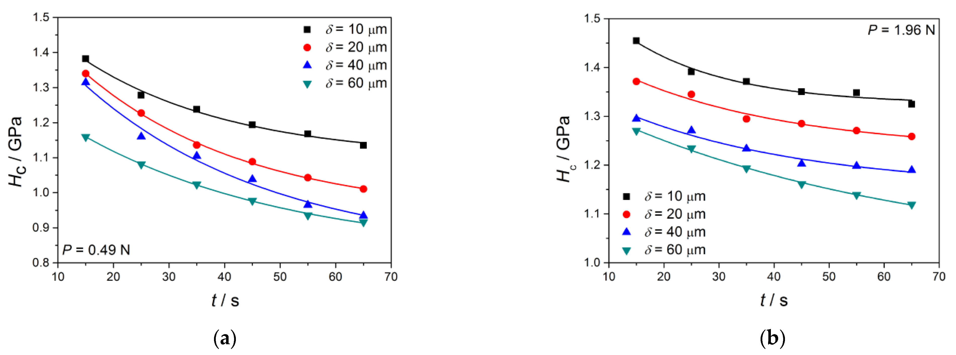
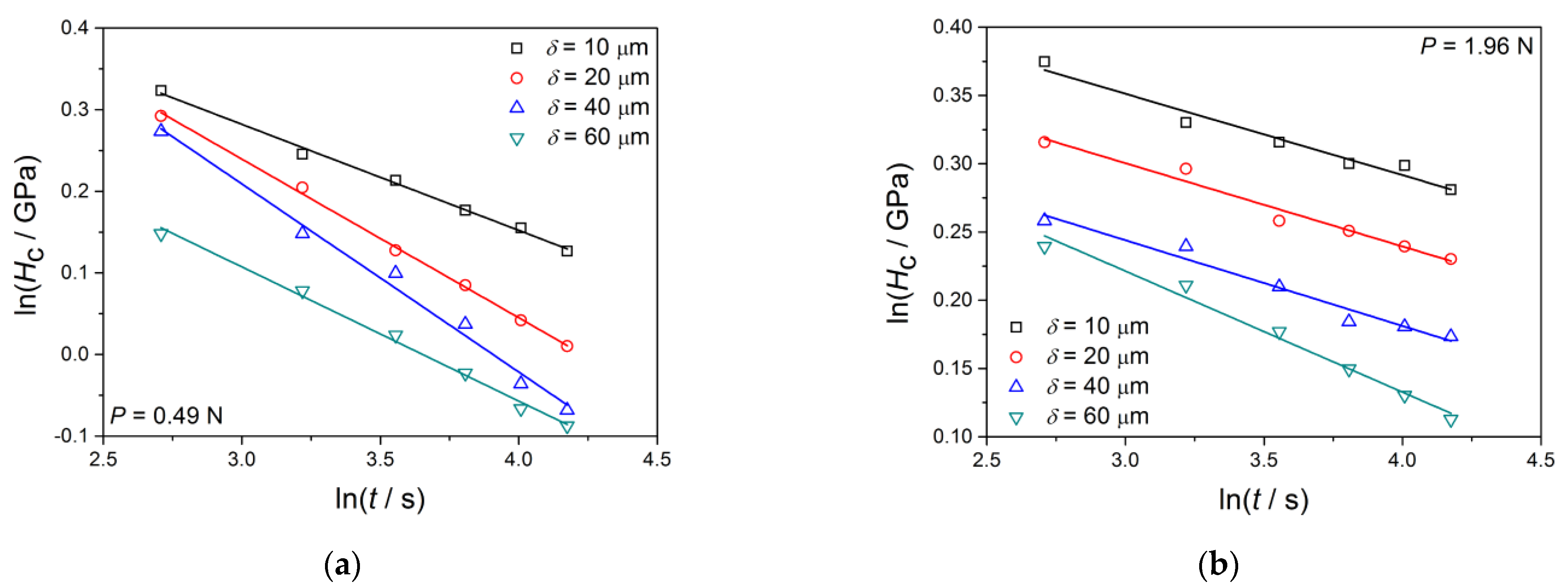
3.2.3. Creep Resistance Analysis of the Cu Coatings

Figure 7 gives the dependencies of the composite hardness on the dwell time for the Cu coatings of various thicknesses obtained with applied loads of 0.49 N (Figure 7a) and 1.96 N (Figure 7b). The decrease in the composite hardness when increasing the dwell time is clearly observed for all thicknesses of the coatings and for both the applied loads.
The main parameter defining the creep resistance characteristics of the coatings is a stress exponent, μ, and this parameter can be determined by the application of the Sargent-Ashby model [47,48]. According to this model, the dependence of Hc on t can be presented by Equation (6):
H c = σ 0 ( c μ ε 0 t ) 1 μ
In Equation (6), ε0 is the strain rate at reference stress σ0, c is constant, t (in s) is dwell time and μ is the stress exponent. The values of the stress exponent around one indicate that the dominant mechanism affecting deformation is diffusion creep; for a value close to 2 it is a grain boundary sliding, and for μ values between 3 and 10 the dominant mechanism is dislocation creep and dislocation climb [48].
The stress exponent can be determined from the linear dependence of ln(Hc) on ln(t) (Figure 8), where the slope of a straight line corresponds to a negative inverse stress exponent (−1/μ). The obtained values of stress exponents are summarized in Table 4.
For an applied load of 0.49 N, the stress exponent decreases with an increase in the coating thickness from 10 to 40 μm. After the minimum was attained with the coating thickness of 40 μm, an increase in the value of this exponent was observed. On the other hand, with the high applied load (1.96 N), the stress exponents for the coatings of thicknesses of 10, 20 and 40 μm were close to each other, and were considerably higher than those obtained at a load of 0.49 N. The value obtained with the 60 μm thick Cu coating was lower, but was still significantly higher than those obtained at the low load.
As such, at the low applied load of 0.49 N, the dominant mechanism is the dislocation creep and the dislocation climb. At the high applied load, the values of the stress exponent that are high and close to each other indicate the existence of some other phenomena, which will be discussed later.

4. Discussion

The Cu coatings’ hardness values in the (0.9418–1.1399) GPa range obtained by application of the C-G model were smaller than the hardness of brass (Hs = 1.41 GPa), confirming the assumption that the coatings of Cu on the brass belong to the “soft film on hard substrate” composite hardness system. The values of the coating hardness were also smaller than those obtained for the Cu coatings on Si(111) produced under the same electrodeposition conditions [25]. For the Cu coatings of thicknesses of 10, 20, 40 and 60 µm, the Hcoat values on Si(111) obtained by application of the C-G model were 2.119, 1.914, 1.5079 and 1.164 GPa, respectively. Comparing the coating hardness values of these two substrates, it is clear that the difference between them decreases with increasing the thickness of the coating.
The largest difference was obtained for the coatings of thickness of 10 µm (about 46%), while the smallest difference was obtained for those the thickness of which was 60 µm (about 19%). This clearly indicates that the difference in the coatings’ hardness values can be attributed to the type of used substrate, i.e., the various contributions of the hardness of the substrate to the determined hardness of the coating. Namely, although both substrates, the Si(111) and the brass B36, belong to the “hard” type of substrates relative to the Cu coatings, the hardness of Si(111) was about five times larger than that of brass B36 (7.42 GPa [20] vs. 1.41 GPa, respectively). Additionally, the measured composite hardness values of the Si(111) substrate were up to 0.70 GPa larger than those of the brass B36, with a tendency for this difference to decrease with the increasing thickness of coating. For the Cu coating, with the thickness of 60 μm, this difference was only about 0.050 GPa. The decrease in the difference in the composite hardness values with increasing the coating thickness is another proof of the strong influence of the substrate hardness, i.e., the type of substrate, on the measured value of the hardness of coatings.
The obtained values for the coating hardness were in line with those found in the literature for electrolytically deposited Cu coatings. The usual values for the hardness of the Cu coatings produced by galvanostatic regimes of electrodeposition were between 0.70 and 1.65 GPa [22,49,50]. The application of electrodeposition at a periodically changing rate led to the formation of Cu coatings with slightly greater hardness than those obtained by the constant galvanostatic regimes. For example, the composite hardness values of the coatings prepared by application of periodically changing regimes, such as the pulsating current (PC) and the reversing current (RC) regimes, were between 1.10 and 2.0 GPa [18]. Ultrasonic-assisted copper electrodeposition in TSV (through silicon via) gave Cu deposits the hardness values of which were between 1.58 and 1.99 GPa [51]. The high hardness value of 2.37 GPa was obtained for jet electrodeposited copper in the PS regime [52]. Aside from regimes of electrodeposition, the parameters affecting the quality, and thus the, hardness of the coatings are composition and type of electrolytes, temperature, the presence of additives in the electrolyte, time, mixing of electrolyte, the type of substrates, etc. [8,53]. Certainly, the substrate type is one of the most important parameters affecting coating hardness, and the approach taken in this investigation enabled us to determine precisely the limiting RID value separating the area where the substrate strongly effects the measured composite hardness from the area in which the measured composite hardness can be considered as the true (absolute) hardness of the coating.
On the other hand, the values of the stress exponent for the Cu coatings electrodeposited on the brass substrate were larger than the corresponding values obtained on the Si(111) substrate. These exponents were between 4.35 and 7.69 for the brass substrate with the load of 0.49 N, while those on the Si(111) substrate were between 2.79 and 5.29 [25] for the same applied load. In the case of the Si(111) substrate, the creep mechanism changed from grain boundary sliding to both dislocation climb and dislocation creep when increasing the thickness of the coatings. For the brass substrate, the dominant mechanism was the dislocation creep and the dislocation climb. The common characteristic for both the substrates was the minimal value of this exponent for the coating of 40 μm thickness.
Then, larger values of the stress exponent were obtained on the brass than on the Si(111) substrate, which caused the change in creep mechanism from the grain boundary sliding to the dislocation climb and the dislocation creep for the Cu coatings electrodeposited on the Si(111) to only the dislocation climb and the dislocation creep for the Cu coatings electrodeposited on the brass, can be discussed as follows: on both the substrates, “soft” copper films of the same characteristics were formed. Simultaneously, the brass was about five times softer than the Si(111) substrate. This means that during the indentation process at the low load, a softer brass substrate provides less resistance to indentation force than the harder Si(111) substrate. This causes the depth of penetration to be greater in the Cu coating formed on the softer brass than on the harder Si(111) substrate. As a final result of this process, the size of the diagonals of the indents was smaller on the surface area of the Cu coatings electrodeposited on the Si(111) than on the brass substrate. For example, at an applied load of 0.49 N, for the 10 µm thick Cu coating, the diagonal is 26.67 µm (Hc = 1.278 GPa) on the brass and 23.36 µm (Hc = 1.665 GPa) on the Si(111) substrate.
Aside from the substrate hardness, the roughness of the coatings is also an important parameter affecting the coating hardness and the stress exponent values. For the 10, 20, 40 and 60 μm thick Cu coatings electrodeposited on the Si(111) substrate, the Ra values of roughness were between 52.42 and 286.3 nm [20]. For the Cu coatings of the same thicknesses electrodeposited on the brass, the Ra values were between 75.05 and 512.03 nm (Table 1), indicating an increase in the roughness between 50 and 100% relative to the Si(111) substrate. This differences can be attributed to the different roughness values of the brass and the Si(111) substrates. Namely, every surface area which represents a cathode, i.e., a substrate for the electrodeposition process, possesses a certain roughness [8]. In our case, the roughness of the brass substrate was considerably greater than that for the Si(111) substrate. As is already known, owing to the production method, the Si(111) substrate represents one of the smoothest substrates.
Now we can additionally explain the various creep mechanisms of the Cu coatings formed on these two substrates. From a macro-morphological point of view, there is no a difference between the Cu coatings electrodeposited on the Si(111) and the brass substrates by the PC regime at the average current density of 50 mA cm−2. Both the deposits are fine-grained, formed in the mixed activation–diffusion control, with a dominant presence of grains of about 5 µm in size. The only difference between these two deposits is the larger number of grains of a size of about 5 µm in the Cu coating electrodeposited on the brass than on the Si(111) substrate. Anyway, the Cu coatings electrodeposited on the Si(111) and the brass substrates represent the typical deposits that have approximately the same coarseness, although are formed on the substrates of various roughness values. The difference in the number of the grains can be attributed to the fact that the initial stage of the electrodeposition processes is determined by the initial state of the electrode surface, i.e., its roughness, while the final morphology of deposits is determined by parameters and the regime of electrodeposition. The substrate of greater roughness contains a larger number of irregularities, with sharp peaks representing preferential sites for the nucleation process and the initial stage of the electrodeposition process. During the deposition process, due to the current density distribution effect, electrodeposition primarily occurs on these sites, i.e., the current density is larger on the peaks than on the other parts of the electrode surface [8]. This process will lead to the formation of deposits with larger number of grains of approximately the same size (about 5.0 μm in our case) on a substrate of greater roughness (the brass) than on that with smaller roughness (the Si(111)). The increase in number of larger grains simultaneously means a decrease in overall number of formed grains, and thus, a decrease in the number of grain boundaries at the surface area of the deposit.
The decrease in the number of grain boundaries is sufficient reason for the change of the creep mechanism from grain boundary sliding to dislocation climb and dislocation creep, characterizing the Cu coatings electrodeposited on the Si(111) substrate, to the dominant dislocation climb and dislocation creep mechanism for those electrodeposited on the brass with an applied load of 0.49 N.
The very high and very close together creep exponents obtained at the Cu coatings of thicknesses of 10, 20 and 40 μm with a high applied load of 1.96 N (16.3 ± 0.50) clearly indicate that these values are determined by the features of the brass as a substrate, but not by the morphological features of Cu deposits. A similar conclusion is also valid for the 60 μm thick Cu coating. In this case, there is some contribution of the Cu deposit to the creep features, but the value of the stress exponent is still high (≈11.3), so we cannot claim to have a relevant value of this exponent for this applied load. As such, the contribution of the substrate to the creep characteristics was predominant for the Cu coating of this thickness.

5. Conclusions

Composite hardness models, such as the Chicot-Lesage (C-L) and the Cheng-Gao (C-G), were used for the determination of the hardness of the Cu coatings from the measured composite hardness. The mechanism of creep resistance was also considered. For the production of Cu coatings of various thicknesses (10, 20, 40 and 60 µm), the PC regime with the following parameters was applied: jav = 50 mA cm−2, jA = 100 mA cm−2, tc = 5 ms, and tp = 5 ms. On the basis of the obtained results, the following conclusions were derived:
o
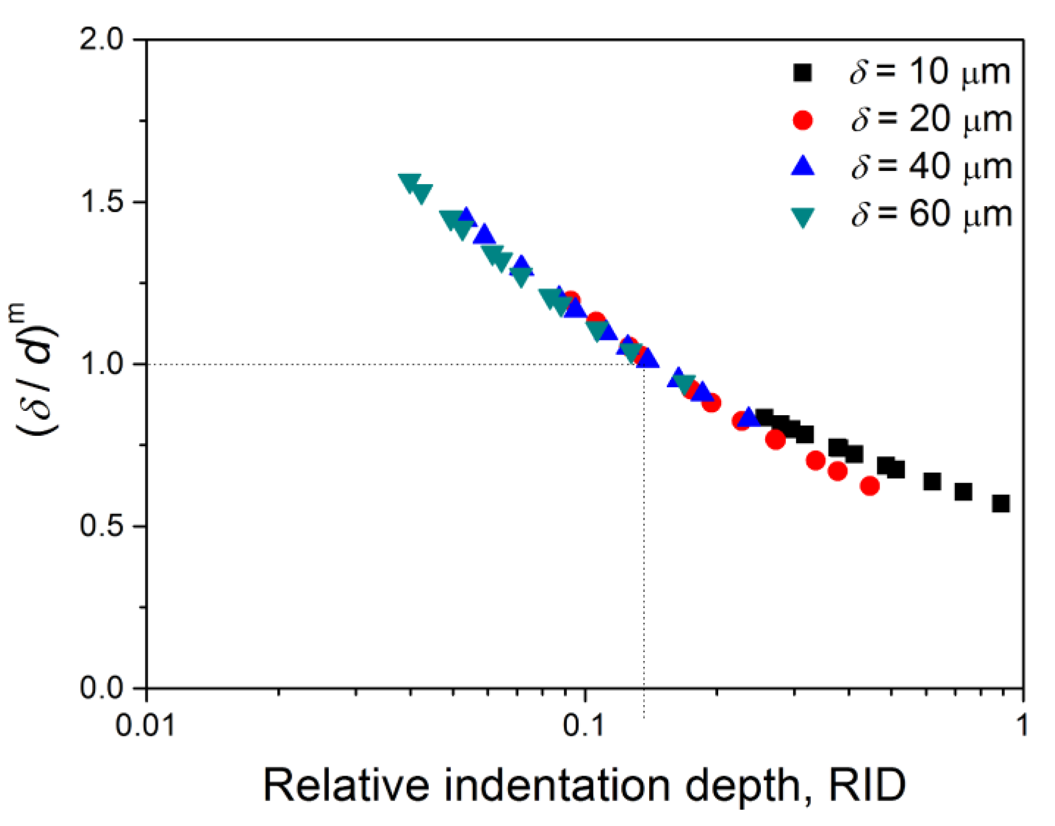
Applying the C-L model, the limiting value of RID of 0.14 was determined for the applied load range. For RID > 0.14, it is necessary to apply the composite hardness model for a determination of the absolute or true coating hardness. For RID < 0.14, the composite hardness corresponds to the coating hardness;
o
The quantification of the values of the coating hardness was done by application of the C-G model. The obtained values between 0.9418 and 1.1399 GPa confirmed the assumption that the coatings of Cu on the brass belongs to the “soft film on hard substrate” composite hardness system;
o
The stress exponents between 4.35 and 7.69 obtained with an applied load of 0.49 N indicated that the dominant creep mechanism is dislocation creep and dislocation climb;
o
By comparison of the obtained morphological and mechanical characteristics of the Cu coatings with those obtained on the Si(111) substrate under the same electrodeposition conditions, the effect of the characteristics of the substrate on the coating hardness and the creep resistance behavior of the coatings has been additionally explained and discussed.

Author Contributions

I.O.M. performed experiments and contributed to the analysis of microhardness; J.S.L. performed analysis of microhardness; D.V.-R. performed the AFM analysis; V.R. contributed in discussion of microhardness measurement; and N.D.N. conceived and wrote the paper. All authors have read and agreed to the published version of the manuscript.

Funding

This work was financially supported by the Ministry of Education, Science and Technological Development of the Republic of Serbia (Grants No. 451-03-68/2020-14/200026 and 451-03-68/2020-14/200135).

Institutional Review Board Statement

Not applicable.

Informed Consent Statement

Not applicable.

Data Availability Statement

The data presented in this study are available on request from the corresponding author or coauthors. The data are not publicly available.

Acknowledgments

This work was funded by Ministry of Education, Science and Technological Development of Republic of Serbia.

Conflicts of Interest

The authors declare no conflict of interest.

References

  1. Copper Plating for Engineering. Available online: https://www.bendplating.com/copper-plating-for-engineering-applications/ (accessed on 1 December 2020).
  2. Wei, H.L.; Huang, H.; Woo, C.H.; Zheng, R.K.; Wen, G.H.; Zhang, X.X. Development of 〈110〉 texture in copper thin films. Appl. Phys. Lett. 2002, 80, 2290–2292. [Google Scholar] [CrossRef] [Green Version]
  3. Miura, S.; Honma, H. Advanced copper electroplating for application of electronics. Surf. Coat. Technol. 2003, 169–170, 91–95. [Google Scholar] [CrossRef]
  4. Elrefaey, A.; Wojarski, L.; Tillmann, W. Preliminary investigation on brazing performance of Ti/Ti and Ti/steel joints using copper film deposited by PVD technique. J. Mater. Eng. Perform. 2012, 21, 696–700. [Google Scholar] [CrossRef]
  5. Jeon, N.L.; Nuzzo, R.G. Physical and spectroscopic studies of the nucleation and growth of copper thin films on polyimide surfaces by chemical vapor deposition. Langmuir 1995, 11, 341–355. [Google Scholar] [CrossRef]
  6. Zheng, B.C.; Meng, D.; Che, H.L.; Lei, M.K. On the pressure effect in energetic deposition of Cu thin films by modulated pulsed power magnetron sputtering: A global plasma model and experiments. J. Appl. Phys. 2015, 117, 203302. [Google Scholar] [CrossRef]
  7. Wei, C.; Wu, G.; Yang, S.; Liu, Q. Electrochemical deposition of layered copper thin films based on the diffusion limited aggregation. Sci. Rep. 2016, 6, 34779. [Google Scholar] [CrossRef] [PubMed] [Green Version]
  8. Popov, K.I.; Djokić, S.S.; Nikolić, N.D.; Jović, V.D. Morphology of Electrochemically and Chemically Deposited Metals; Springer International Publishing: New York, NY, USA, 2016. [Google Scholar] [CrossRef]
  9. Nikolić, N.; Stojilković, E.; Djurović, D.; Pavlović, M.; Knežević, V. The preferred orientation of bright copper deposits. Mater. Sci. Forum 2000, 352, 73–78. [Google Scholar] [CrossRef]
  10. Tantavichet, N.; Damronglerd, S.; Chailapakul, O. Influence of the interaction between chloride and thiourea on copper electrodeposition. Electrochim. Acta 2009, 55, 240–249. [Google Scholar] [CrossRef]
  11. Song, S.J.; Choi, S.R.; Kim, J.G.; Kim, H.G. Effect of molecular weight of polyethylene glycol on copper electrodeposition in the presence of bis-3-sulfopropyl-disulfide. Int. J. Electrochem. Sci. 2016, 151, 10067–10079. [Google Scholar] [CrossRef]
  12. Moffat, T.P.; Wheeler, D.; Josell, D. Electrodeposition of copper in the SPS-PEG-Cl additive system I. Kinetic measurements: Influence of SPS. J. Electrochem. Soc. 2004, 151, C262–C271. [Google Scholar] [CrossRef]
  13. Bozzini, B.; D’Urzo, L.; Romanello, V.; Mele, C. Electrodeposition of Cu from acidic sulfate solutions in the presence of bis-(3-sulfopropyl)-disulfide (SPS) and chloride ions. J. Electrochem. Soc. 2006, 153, C254–C257. [Google Scholar] [CrossRef] [Green Version]
  14. Nikolić, N.; Rakočević, Z.; Popov, K. Structural characteristics of bright copper surfaces. J. Electroanal. Chem. 2001, 514, 56–66. [Google Scholar] [CrossRef]
  15. Nikolic, N.D.; Rakočević, Z.; Popov, K.I. Reflection and structural analyses of mirror-bright metal coatings. J. Solid State Electrochem. 2004, 8, 526–531. [Google Scholar] [CrossRef]
  16. Pasquale, M.; Gassa, L.; Arvia, A. Copper electrodeposition from an acidic plating bath containing accelerating and inhibiting organic additives. Electrochim. Acta 2008, 53, 5891–5904. [Google Scholar] [CrossRef] [Green Version]
  17. Marro, J.B.; Darroudi, T.; Okoro, C.A.; Obeng, Y.S.; Richardson, K. The influence of pulse plating frequency and duty cycle on the microstructure and stress state of electroplated copper films. Thin Solid Films 2017, 621, 91–97. [Google Scholar] [CrossRef] [Green Version]
  18. Kristof, P.; Pritzker, M. Improved copper plating through the use of current pulsing & ultrasonic agitation. Plat. Surf. Finish. 1998, 85, 237–240. Available online: http://www.nmfrc.org/pdf/9811237.pdf (accessed on 5 December 2020).
  19. Tantavichet, N.; Pritzker, M.D. Effect of plating mode, thiourea and chloride on the morphology of copper deposits produced in acidic sulphate solutions. Electrochim. Acta 2005, 50, 1849–1861. [Google Scholar] [CrossRef]
  20. Mladenović, I.; Lamovec, J.S.; Radović, D.V.; Vasilić, R.; Radojevic, V.; Nikolić, N.D. Morphology, structure and mechanical properties of copper coatings electrodeposited by pulsating current (PC) regime on Si(111). Metals 2020, 10, 488. [Google Scholar] [CrossRef] [Green Version]
  21. MladenoviĆ, I.O.; Lamovec, J.S.; Jović, V.B.; Obradov, M.; Radović, D.V.; Nikolić, N.D.; Radojević, V.J. Mechanical characterization of copper coatings electrodeposited onto different substrates with and without ultrasound assistance. J. Serbian Chem. Soc. 2019, 84, 729–741. [Google Scholar] [CrossRef] [Green Version]
  22. Martins, L.; Martins, J.; Romeira, A.; Costa, M.E.V.; Costa, J.S.; Bazzaoui, M. Morphology of copper coatings electroplated in an ultrasonic field. Mater. Sci. Forum 2004, 455–456, 844–848. [Google Scholar] [CrossRef]
  23. Mallik, A.; Ray, B.C. Morphological study of electrodeposited copper under the influence of ultrasound and low temperature. Thin Solid Films 2009, 517, 6612–6616. [Google Scholar] [CrossRef]
  24. Bull, S.J. Microstructure and indentation response of TiN coatings: The effect of measurement method. Thin Solid Films 2019, 688, 137452. [Google Scholar] [CrossRef]
  25. Mladenović, I.O.; Lamovec, J.S.; Vasiljević-Radović, D.G.; Radojević, V.J.; Nikolić, N.D. Mechanical features of copper coatings electrodeposited by the pulsating current (PC) regime on Si(111) substrate. Int. J. Electrochem. Sci. 2020, 148, 12173–12191. [Google Scholar] [CrossRef]
  26. Burnett, P.; Rickerby, D. The mechanical properties of wear-resistant coatings. II: Experimental studies and interpretation of hardness. Thin Solid Films 1987, 148, 51–65. [Google Scholar] [CrossRef]
  27. Bull, S.; Rickerby, D. New developments in the modelling of the hardness and scratch adhesion of thin films. Surf. Coat. Technol. 1990, 42, 149–164. [Google Scholar] [CrossRef]
  28. Lesage, J.; Pertuz, A.; Chicot, D. A new method to determine the hardness of thin films. Matéria 2004, 9, 13–22. Available online: http://www.materia.coppe.ufrj.br/sarra/artigos/artigo10294 (accessed on 7 December 2020).
  29. Lesage, J.; Pertuz, A.; Puchi-Cabrera, E.; Chicot, D. A model to determine the surface hardness of thin films from standard micro-indentation tests. Thin Solid Films 2006, 497, 232–238. [Google Scholar] [CrossRef]
  30. Lesage, J.; Chicot, D.; Pertuz, A.; Jouan, P.Y.; Horny, N.; Soom, A. A model for hardness determination of thin coatings from standard micro-indentation tests. Surf. Coat. Technol. 2005, 200, 886–889. [Google Scholar] [CrossRef]
  31. Chicot, D.; Lesage, J. Absolute hardness of films and coatings. Thin Solid Films 1995, 254, 123–130. [Google Scholar] [CrossRef]
  32. Chen, M.; Gao, J. The adhesion of copper films coated on silicon and glass substrates. Mod. Phys. Lett. B 2000, 14, 103–108. [Google Scholar] [CrossRef]
  33. He, J.L.; Li, W.Z.; Li, H.D. Hardness measurement of thin films: Separation from composite hardness. Appl. Phys. Lett. 1996, 69, 1402–1404. [Google Scholar] [CrossRef]
  34. Hou, Q.; Gao, J.; Li, S. Adhesion and its influence on micro-hardness of DLC and SiC films. Eur. Phys. J. B 1999, 8, 493–496. [Google Scholar] [CrossRef]
  35. Magagnin, L.; Maboudian, R.; Carraro, C. Adhesion evaluation of immersion plating copper films on silicon by microindentation measurements. Thin Solid Films 2003, 434, 100–105. [Google Scholar] [CrossRef]
  36. Korsunsky, A.M.; McGurk, M.R.; Bull, S.J.; Page, T.F. On the hardness of coated systems. Surf. Coat. Technol. 1998, 99, 171–183. [Google Scholar] [CrossRef]
  37. Tuck, J.R.; Korsunsky, A.M.; Bull, S.J.; Davidson, R.I. On the application of the work-of-indentation approach to depth-sensing indentation experiments in coated systems. Surf. Coat. Technol. 2001, 137, 217–224. [Google Scholar] [CrossRef]
  38. Lamovec, J.; Jović, V.; Randjelović, D.; Aleksić, R.; Radojevic, V. Analysis of the composite and film hardness of electrodeposited nickel coatings on different substrates. Thin Solid Films 2008, 516, 8646–8654. [Google Scholar] [CrossRef]
  39. Ma, Z.; Zhou, Y.; Long, S.; Lu, C. On the intrinsic hardness of a metallic film/substrate system: Indentation size and substrate effects. Int. J. Plast. 2012, 34, 1–11. [Google Scholar] [CrossRef] [Green Version]
  40. Chudoba, T.; Richter, F. Investigation of creep behaviour under load during indentation experiments and its influence on hardness and modulus results. Surf. Coat. Technol. 2001, 148, 191–198. [Google Scholar] [CrossRef]
  41. ASTM E384—16: Standard Test Method for Microindentation Hardness of Materials; ASTM International: West Conshohocken, PA, USA, 2016; Available online: https://www.astm.org/DATABASE.CART/HISTORICAL/E384-16.htm (accessed on 1 December 2020).
  42. ISO 6507-1-2005: Metallic Materials—Vickers Hardness Test—Part 1: Test Method; International Organization for Standardization: Geneva, Swizterland, 2005; Available online: https://www.iso.org/standard/37746.html (accessed on 1 December 2020).
  43. Li, H.; Bradt, R.C. Knoop microhardness anisotropy of single-crystal LaB6. Mater. Sci. Eng. A 1991, 142, 51–61. [Google Scholar] [CrossRef]
  44. Buckle, H. The Science of Hardness Testing and Its Research Applications; Westbrook, J.W., Conrad, H., Eds.; American Society for Metals: Metals Park, OH, USA, 1973; p. 453. [Google Scholar]
  45. Lamovec, J.; Jovic, V.; Aleksic, R.; Radojevic, V. Micromechanical and structural properties of nickel coatings electrodeposited on two different substrates. J. Serbian Chem. Soc. 2009, 74, 817–831. [Google Scholar] [CrossRef]
  46. Petrík, J.; Blaško, P.; Vasilňaková, A.; Demeter, P.; Futáš, P. Indentation size effect of heat treated aluminum alloy. Acta Met. Slovaca 2019, 25, 166–173. [Google Scholar] [CrossRef] [Green Version]
  47. Sargent, P.M.; Ashby, M.F. Indentation creep. Mater. Sci. Technol. 1992, 8, 594–601. [Google Scholar] [CrossRef]
  48. Farhat, S.; Rekaby, M.; Awad, R. Vickers microhardness and indentation creep studies for erbium-doped ZnO nanoparticles. SN Appl. Sci. 2019, 1, 546. [Google Scholar] [CrossRef] [Green Version]
  49. Kasach, A.A.; Kurilo, I.; Kharitonov, D.S.; Radchenko, S.L.; Zharskii, I.M. Sonochemical electrodeposition of copper coatings. Russ. J. Appl. Chem. 2018, 91, 207–213. [Google Scholar] [CrossRef]
  50. Tao, S.; Li, D.Y. Tribological, mechanical and electrochemical properties of nanocrystalline copper deposits produced by pulse electrodeposition. Nanotechnology 2006, 17, 65–78. [Google Scholar] [CrossRef]
  51. Wang, F.; Yang, Y.; Wang, Y.; Ren, X.; Li, X. Study on physical properties of ultrasonic-assisted copper electrodeposition in through silicon via. J. Electrochem. Soc. 2020, 167, 022507. [Google Scholar] [CrossRef]
  52. Fan, H.; Zhao, Y.; Jiang, J.; Wang, S.; Shan, W.; Li, Z. Effect of the pulse duty cycle on the microstructure and properties of a jet electrodeposited nanocrystalline copper coating. Mater. Trans. 2020, 61, 795–800. [Google Scholar] [CrossRef]
  53. Pena, P.E.M.D.; Roy, S. Electrodeposited copper using direct and pulse currents from electrolytes containing low concentration of additives. Surf. Coat. Technol. 2018, 339, 101–110. [Google Scholar] [CrossRef] [Green Version]
Figure 1. Morphology of the copper coating electrodeposited on the brass by the PC regime at a jav of 50 mA cm−2. The thickness of the coating: 40 μm. The parameters of the PC regime: tc = 5 ms, tp = 5 ms and jA = 100 mA cm−2 ((a) ×1000, and (b) ×3000).
Metals 11 00111 g001
Figure 2. The surface topography and the line section analysis of the Cu coatings of thicknesses from: (a) 10 μm, (b) 20 μm, (c) 40 μm, and (d) 60 μm. Scan size: (70 × 70) μm2.
Metals 11 00111 g002aMetals 11 00111 g002b
Figure 3. Cross section analysis of the Cu coatings electrodeposited by the PC regime on the brass of thicknesses from: (a) 10 µm, (b) 20 µm, (c) 40 µm, and (d) 60 µm.
Metals 11 00111 g003
Figure 4. Determination of the absolute (true) hardness of the brass B36 substrate.
Metals 11 00111 g004
Figure 5. The dependencies of (a) the composite hardness, and (b) the coating hardness, on the RID (relative indentation depth) for the Cu coatings of thicknesses of 10, 20, 40 and 60 μm, obtained by the PC regime at a jav of 50 mA cm−2. The coating hardness was calculated by application of the Chicot–Lesage (C–L) model.
Metals 11 00111 g005
Figure 6. The dependencies of the (δ/d)m on the RID obtained for the 10, 20, 40 and 60 µm thick Cu coatings.
Metals 11 00111 g006
Figure 7. The dependencies of the composite hardness (Hc) on the dwell time (t) for the 10, 20, 40 and 60 μm thick Cu coatings obtained by the PC regime with an applied load of (a) 0.49 N and (b) 1.96 N.
Metals 11 00111 g007
Figure 8. The dependencies of ln(Hc) on ln(t) for the 10, 20, 40 and 60 μm thick Cu coatings obtained by the PC regime with an applied load of (a) 0.49 N and (b) 1.96 N.
Metals 11 00111 g008
Table 1. The values of the arithmetic average of the absolute (Ra) roughness with a standard deviation of the Cu coatings of various thicknesses. Scan size: (70 × 70) μm2.
δ/μm10204060
Ra/nm75.05 ± 8.1146.0 ± 7.83215.6 ± 8.62512.03 ± 3.93
Table 2. The values of exponent m and regression coefficient R2, for the Cu coatings of various thicknesses.
δ/µm10204060
m0.30820.41410.37440.3506
R20.91850.97670.95890.9332
Table 3. The values of fitting parameters (A, B and C), error fitting (RMSE—root mean square error) and the coating hardness (Hcoat) obtained by application of the Cheng-Gao (C-G) model for the 10, 20, 40 and 60 μm thick Cu coatings obtained on the brass substrate by the PC regime at a jav of 50 mA cm−2.
δ/μmABCRMSEHcoat/GPa
101.14820.24−66470.087681.1399
201.147.138−14570.10181.1295
401.34−2.575−1090.055911.1180
600.951320.01−49060.07210.9418
Table 4. The values of the stress exponent (μ) obtained for the Cu coatings thicknesses of 10, 20, 40 and 60 μm with applied loads of 0.49 and 1.96 N.
The Thickness of Coatings/μmThe Stress Exponent (μ) Obtained with Applied Load (P in N) of:
0.49 1.96
107.6916.78
205.1416.39
404.3515.90
606.0111.28
Publisher’s Note: MDPI stays neutral with regard to jurisdictional claims in published maps and institutional affiliations.

