
Abstract
Van der Waals heterostructures based on hexagonal boron nitride (h-BN) and other 2D materials may pave the way for future electronic applications. Wafer-scale uniform h-BN substrates are a must in this respect. In this work, we demonstrate a new growth regime which allows for scalable, uniform synthesis of high quality h-BN layers on 2' sapphire substrates. We propose a new approach to metal organic vapour phase epitaxy of h-BN layers on sapphire substrates. The growth scheme involves an intermediary BN buffer layer grown under self-limiting conditions (continuous flow) followed by the final growth of h-BN with flow modulated epitaxy in one growth run. This scheme can be regarded as homoepitaxial growth of h-BN on a self-limiting buffer. Our studies show that the buffer layer allows to control the nucleation at the crucial early stages of BN layer growth, suppressing unwanted out-of-plane growth. It can also be used to control the density of point-like defects responsible for unwanted luminescence from the h-BN layer. Moreover, our results show that the buffer effectively suppresses the creation of amorphous BN at the sapphire/h-BN interface.
Export citation and abstract BibTeX RIS

Original content from this work may be used under the terms of the Creative Commons Attribution 4.0 license. Any further distribution of this work must maintain attribution to the author(s) and the title of the work, journal citation and DOI.
1. Introduction
BN layers consisting of a honeycomb lattice made of boron and nitrogen atoms are of increasing interest for future electronic applications. Because of the wide band gap (∼6 eV) and the two-dimensional character, h-BN is an ideal insulating barrier material in devices based on van der Waals heterostructures [1, 2] Moreover, h-BN is an excellent substrate for other two-dimensional materials [3, 4], a platform for single photon emitters [5] and bears great hope for future application in DUV (Deep-Ultraviolet) lighting [6]. The growth of wafer-scale h-BN on appropriate substrates with excellent control of the thickness and crystalline quality are the prerequisites for successful application. BN layers were grown on several different substrates, with mixed success on metallic templates (Ru, Ni, Cu, Pt, Fe, Rh, Au) as well as on Si-SiO2, SiC and sapphire [7–15] A summary of the growth techniques and properties of various sp2-BN species can be found in the works of K Zhang et al[ 13] and A Pakdel et al[ 16]. Discussions of various growth parameters governing MOVPE/MOCVD techniques were also reported [17, 18]. Flow modulation epitaxy (FME) on sapphire substrates, for which the precursor gases are introduced in the growth chamber in an alternating manner, seems to be at the moment one of the most promising approaches to the challenge of h-BN growth [19, 20]. Although growth in the continuous flow growth (CFG) regime, for which the precursor gases are introduced simultaneously into the growth reactor, may have some advantages, it shows a self-limiting behaviour [18] suitable only for ultra-thin layers. The development of growth techniques that allow to grow high quality, wafer-scale van der Waals materials, especially h-BN, is one of the most studied subjects in growth technology at the moment. First steps into this direction were already reported for sapphire [21–23] and nickel substrates [15]. An important aspect after growth is to analyse the wafer-scale h-BN layer to be sure that the layer is spatially uniform and that values like the lattice parameters of the crystal structure are consistent. Moreover, there is still another important question, which was so far largely ignored in literature, namely whether the final BN layer has a hexagonal (h-BN) structure with AA'-stacking or rhombohedral (r-BN) structure with ABC stacking.
The properties of the substrate, such as the surface morphology and lattice mismatch are one of the most important parameters for MOVPE processes. Some attempts to change these properties by growing intermediate layers on sapphire substrates were already attempted. Examples include graphene [24], very recently copper [25] and AlN [26]. Lately X Yang et al[ 26] reported that intentional growth of AlN as intermediate layer on sapphire is another way towards wafer-scale h-BN growth. X-ray diffraction results show a FWHM (full width at half maximum) of the BN diffraction peak of around 500 s of arc. Growth of sp2-BN on an AlN sublayer was already reported by Chubarov et al[ 27], but it was concluded, that most probably, a r-BN type structure was grown in such a system.
An analysis of the reports for BN grown on sapphire that present x-ray diffraction results, as well as our own experimental experience, show that AlN is always present as nonintentional intermediary material at the sapphire-BN boundary. The fingerprint of such layers is the x-ray data showing a wide 'bump' between the h-BN peak position at around 26° and sharp peak coming from sapphire substrate diffraction at 41.7° [20, 28]. The thickness of such a nonintentional AlN layer is in the range of 0–2 nm. The maximum of this 'bump' at an angular position of 36.04° agrees well with the AlN 0002 x-ray diffraction position [29]. A combination of AlN and a low temperature (800 °C) BN intermediate layer was also already used [30]. The discussed approaches all involve foreign material (Cu, AlN). To eliminate a possible influence of AlN and Cu on the final sp2-BN layer we propose to use self-limiting CFG buffer layer of sp2-BN as part of the full process.
In this work we report on high quality wafer-scale sp2-BN, grown by MOVPE on sapphire using a transitional sp2-BN CFG layer as the immediate substrate for the final BN growth. The intermediate BN layer was grown by CFG and the final sp2-BN layer was grown in the same growth run by using the FME mode. This in a way can be considered as a homoepitaxial BN growth giving rise to high quality h-BN layers with scalable thickness.
2. Methods
2.1. Sample growth
Boron nitride (sp2-BN) layers were obtained by MOVPE using an Aixtron CCS 3 × 2'' reactor equipped with an ARGUS Thermal Mapping System to directly control the substrate temperature. Growth was performed on two-inch sapphire c-plane wafers (with up to 0.2° misorientation) as a substrate. Ammonia and triethylboron (TEB) were used as the precursors for nitrogen and boron, respectively, the carrier gas was hydrogen. The system temperature set in the MOVPE reactor and controlled via thermocouple was the same (1575 °C) for all the samples and growth stages. The device is equipped with two growth monitoring systems. Firstly, an optical reflectometer, using a laser with 635 nm wavelength that allows to monitor the reflection from the growing material. Secondly, the multipoint pyrometer (ARGUS), which was used to read the real temperature distribution on the upper surface of the susceptor holding the substrate wafers, showing that temperature control based on thermocouple is not a reliable source of data. One should bear in mind that throughout this paper the reading from the pyrometer will be used as growth temperature. Five samples were obtained by combined two-stage epitaxial growth. The growth process of the intermediate BN layer was performed using the CFG method, where precursors enter the reactor simultaneously. The second BN layer is formed by the FME method—the alternate switching of ammonia and TEB flows. The main difference between samples investigated in this study is the time of the CFG—stage growth: 15 min (sample S15), 30 min (sample S30), 60 min (samples SI+II and S60) and 90 min (sample S90). The results obtained for these samples are compared with samples SI( 60 min of CFG—stage growth only) and SII( the FME—stage growth directly on sapphire). The FME growth stage was kept the same for all the samples grown to cut down the number of parameters in the study.
The best quality CFG samples can be obtained for a high V/III ratio and high temperature, unfortunately those conditions also promote self-limiting growth [18]. It is possible to obtain maximally a few nanometres of continuous, wafer-scale BN layers with good optical and structural properties. The prolongation of the growth, in this mode, results in the appearance of free-standing, randomly oriented BN flakes that dominate the growth after a sufficiently long time [18]. The growth temperature of the intermediate stage in our study was 1305 °C–1315 °C and the TEB flow 10 ccm.
The FME method allows to achieve thicker, continuous BN layers reaching up to hundreds of nm. However, this mode is burdened by the inherent temporary ammonia deficiency which results in the formation of structural defects. The structural and optical properties of the samples grown by this method are incomparably better than CFG samples in the case of thicker BN layers. This behaviour is explained by the initial nucleation process [26] before the correct stacking of the subsequent layers. Growth of such BN layer on a high quality CFG buffer should help to avoid this nucleation step and allow to start the immediate growth of already properly ordered material. The growth temperature of this final stage was 1295 °C–1310 °C and the TEB flow was up to 15 ccm in the pulse. Basic growth parameters are listed in table 1.
Table 1. Growth parameters as set (time, TEB flow) or measured (temperature by ARGUS) for the samples presented in the study.
| Sample | Growth temperature (°C) | TEB flow (ccm) | Growth mode | Time of CFG and FME stage growth (min) |
|---|---|---|---|---|
| SI | 1305 | 10 | CFG | 60 |
| SII | 1295 | 0–15 | FME | 60 |
| SI+II | 1315 | 10 | CFG | 60 |
| 1310 | 0–15 | FME | 60 | |
| S15 | 1310 | 10 | CFG | 15 |
| 1300 | 0–15 | FME | 60 | |
| S30 | 1305 | 10 | CFG | 30 |
| 1300 | 0–15 | FME | 60 | |
| S60 | 1305 | 10 | CFG | 60 |
| 1300 | 0–15 | FME | 60 | |
| S90 | 1305 | 10 | CFG | 90 |
| 1300 | 0–15 | FME | 60 |
2.2. Experimental techniques
The morphology of the samples was examined by atomic force microscopy (AFM) and scanning electron microscopy (SEM) (FEI Helios NanoLab 600). Raman scattering was measured using a Renishaw inVia system with a 532 nm laser line using continuous wave Nd-YAG laser as an excitation source. The photoluminescence was excited with a 473 nm laser source and a LabRAM HR800 (Horiba Jobin Yvon) Raman spectrometer with a charge-coupled device detector cooled by Peltier modulus. The spectrum was collected through a 100x objective (NA 0.9) by a Olympus BX61 confocal microscope.Throughout this study a X'Pert Panalitical setup have been used for x-ray experiments. A standard laboratory CuKα x-ray source conditioned by a x-ray mirror for Bragg–Brentano optics or 4-bounce Hart–Bartels crystal monochromator-conditioner for High Resolution x-ray Diffraction optics were employed. Our x-ray diffraction 2theta/omega scans were performed under the symmetrical Bragg–Brentano diffraction conditions utilizing the crystallographic planes parallel to the main substrate plane. This means that we are probing the inter-planar spacing of the BN layer along the c-axis of the stack parallel to the main substrate plane. We have also performed x-ray diffraction experiments in the high resolution mode utilizing symmetrical 0002 and 0004 h-BN Bragg reflections, with x-ray optics involving a Hart–Bartels type incident beam monochromator and an analyser in front of the x-ray counter. Infrared reflectance spectra were also measured using a FTIR microscope (Thermo Fischer Scientific iS50, Nicolet Continuum) equipped with a 32x infinity corrected reflective objective (NA 0.65).
3. Results and discussion
3.1. Morphology
Surface images, as shown in figure 1 compare the samples grown with CFG, FME and the CFG + FME final sample. The final sample SI+II is comprising the two processes in one run. Real process temperatures are as measured on the susceptor with ARGUS system (table 1). An AFM image for sample SI was combined with the SEM image for this CFG sample to show that the wrinkle pattern of top surface is present in all cases indicating the continuous overgrowth of the underlying substrate (see full AFM image in figure S1 available online at https://stacks.iop.org/2DM/8/015017/mmedia). The well-known wrinkle pattern shows the largest mesh size for the final CFG and FME sample suggesting a larger uniformity of the layer across the sample in this combined process.
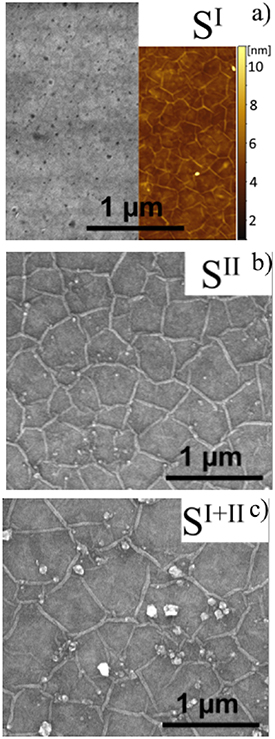
Figure 1. (a) Combined SEM and AFM images of the surface of a) CFG only process (sample SI).(b) SEM of a FME only process (sample SII).(c) SEM result of a CFG + FME process (sample SI+II). Growth temperatures for sample SI+II CFG 1315 °C and 1310 °C FME stages respectively.
Download figure:
Standard image High-resolution imageOne of the problems with the sp2-BN layers grown on sapphire substrates is the presence of the secondary out-of-plane nucleation centres which result in the debris islands present on the top surface [17, 20] or affecting the overall growth process [19]. As can be inferred from the sample series in figure 2 secondary out-of-plane nucleation can be controlled by the CFG stage growth time, where for 15 min one can observe minimal density of such debris in the final sample. The wrinkle mesh pattern is almost the same for all samples suggesting that the mesh size is connected to the growth time (i.e. thickness) of the final FME stage, but the interaction with and influence by the out-of-plane secondary nucleation centres may not be excluded (sample S90).
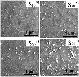
Figure 2. SEM of 2 stage processes (CFG + FME), with different buffer time growth (a) (S15) 15 min CFG stage, (b) (S30) 30 min CFG stage, (c) (S60) 60 min CFG stage (d) (S90) 90 min CFG stage.
Download figure:
Standard image High-resolution image3.2. Raman measurement
Raman spectroscopy is a fast and simple method to confirm that the obtained material is sp2-hybridized BN. The characteristic E2g signal from in-plane vibrations of boron and nitrogen atoms at about 1367 cm−1[ 31] was observed for all the samples. This result confirms the growth of the well-organized sp2-BN and is illustrated on figure 3. Our recorded Raman spectra also show a photoluminescence background that increases for larger Raman shifts. The result can be seen on the figure 3 especially for sample SII, which shows the highest photoluminescence signal. This background is usually ascribed to the presence of point-like defects in the BN structure [18, 20, 32]. The weak intensity of the BN Raman peak for sample SI is simply connected to the thickness of this layer (about 3 nm). For all other samples the intensities of the E2g Raman mode are very similar. The recorded variable background results from the presence of a different density of point-like defects in the BN layer (more detailed discussion in sub-section 3.3).

Figure 3. Raman spectra of all samples showing a characteristic peak around 1367 cm−1 indicating the presence of sp2-BN layer. The additional signal at 749 cm−1 comes from the sapphire substrate [33].
Download figure:
Standard image High-resolution image3.3. Photoluminescence measurement
The intensity and the shape of the spectrum for sample SII shown in figure 4, with the main peak at about 2.26 eV and phonon replicas at about 2.08 eV and 1.94 eV is characteristic for all the samples obtained solely by FME and correlates with the excess of TEB during the growth [20]. It is associated with the incorporation of carbon in the place of nitrogen and boron [18, 20, 32] or its various complexes with hydrogen, boron or nitrogen monovacancies [34]. The photoluminescence signal observed for the FME sample SII is almost twice as large as compared to all other samples. Capping the sapphire substrate with the specific CFG buffer layer may lead to the control of the unwanted presence of the lattice point defects likely to be carbon or different types of vacancies. The thinnest CFG samples always have both good structural and optical properties (sample SI, CFG only). Growing exactly the same FME layer on the top of the CFG buffer not only causes a better arrangement of monolayers relative to each other but also reduces the number of defects responsible for this kind of luminescence. This relationship shows that improving the structural properties will also help to eliminate the midgap luminescence.
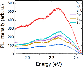
Figure 4. Photoluminescence spectra indicating a variable density of point-like defects. Sample SI( thin CFG buffer only) shows the lowest signal. Sample SII( only FME, no CFG buffer) shows the largest PL signal. The remaining samples were grown using the two-stage approach and although the FME process parameters were the same, the resulting intensities are significantly lower than compared to sample SII.
Download figure:
Standard image High-resolution image3.4. X-ray diffraction and reflectometry
The technique to answer the structural quality problem (wafer-scale uniformity and lattice parameter conformity across the wafer) which seems to be most appropriate, is x-ray diffraction. The FWHM of the diffraction peak as well as angular position of the peak may reveal the basic crystal structure of the layer. As far as the x-ray peak position is concerned, sp2-BN has unfortunately two closely positioned structures, h-BN and r-BN, with the respective 0002/0003 peak positions 26.76° and 26.72° [35]. Structures of h-BN and r-BN have fundamentally different stacking sequences. The structure of h-BN has an AA' stacking sequence and r-BN an ABC sequence [31, 36]. The FWHM of the diffraction peak in the ideal case is in the range of seconds of arc for thick layers (tens of nm). Anything in the range of few hundred seconds of arc for layers of such thickness may imply a composition of h-BN, r-BN and a turbostratic addition (t-BN).
To gain full insight into the total thickness of the material grown on sapphire one can use x-ray reflectometry (XRR), which does not use the standard Bragg diffraction (XRD) condition but utilizes the x-ray scattering just above the total reflection range. The total thicknesses from XRR measurements have to be confronted with the XRD thickness estimates. The XRD thickness was calculated using the classic Scherrer formula [37] which incorporates the FWHM of the peak. Diffraction results (FWHM of the peak) give a thickness estimate of the crystallographic part of the layer for both t-BN, r-BN and h-BN species. Despite the simplicity of the Scherrer formula it yields very good estimates of the thickness of well-stacked crystallographic planes (as in sp2-BN) given by diffraction related signal.
3.4.1. 2theta/omega scan
Our x-ray diffraction 2theta/omega scans were performed using the symmetrical Bragg–Brentano diffraction conditions utilizing the crystallographic planes parallel to the main substrate plane. This means that we are probing inter-planar spacing of the BN layer along the c-axis of the stack around the 0002 h-BN and 0003 r-BN x-ray reflections. The 2theta peak positions for respective h-BN and r-BN reflections are 26.76/26.72 deg. which are very difficult to distinguish. So in this study we have assumed that they merge into a single peak and the Scherrer formula estimates the thickness of such a collective structure. Respective results of the x-ray 2theta/omega scans are shown in figure 5. It can be easily seen that the scan for sample SI is characterized by a wide distribution consisting of a single peak, but the rest of the curves show two distinct peaks. These scans can be easily fitted by two Gaussians where the peak denoted with A in table 2 constitutes the left hand shoulder of the distribution and B is the most intense right hand side part (figure S2). We ascribe peak A to the turbostratic BN layer and peak B to the h-BN/r-BN collective structure, if present. The obtained values for the FWHM and peak positions (table S1) were used to estimate the diffraction connected inter-planar spacing's and thicknesses via the Scherrer formula. From XRR results one can estimate the total thickness of the material grown on the initial substrate utilizing the well-known Kiessig fringes [38] recorded in the low angle scattering of x-rays. We have used a standard x-ray Reflectivity software package (Panalytical) to analyse and model the experimental results (figure S3).

Figure 5. x-ray diffraction 2theta/omega scans for the studied set of samples.
Download figure:
Standard image High-resolution imageTable 2. Lattice parameters and results of estimates of the thickness for the samples studied. A-peak on the left hand part of the recorded curve, B—peak on the right hand side both resolved by fitting Gaussian profiles. XRR estimated thickness (Kiessig fringes fits). FTIR estimated thickness.
| Sample | Inter-planar spacing (Å) | XRD Scherrer thickness (nm) | XRR thickness (nm) | FTIR thickness (nm) |
|---|---|---|---|---|
| SI | 3.45 | 3.32 (t-BN) | 2.7 | 1.4 |
| SII | A 3.41 B 3.36 | A 6.72 (t-BN) B 16.34 (sp2-BN) | 36.6 | 30.5 |
| SI+II | A 3.38 B 3.34 | A 6.94 (t-BN) B 21.62 (sp2-BN) | 38.5 | 35.7 |
| S15 | A 3.38 B 3.34 | A 7.32 (t-BN) B 20.74 (sp2-BN) | 30.8 | 29.9 |
| S30 | A 3.38 B 3.34 | A 7.36 (t-BN) B 19.98 (sp2-BN) | 27.1 | 26.3 |
| S60 | A 3.38 B 3.34 | A 6.82 (t-BN) B 20.38 (sp2-BN) | 32.6 | 31.2 |
| S90 | A 3.38 B 3.34 | A 6.38 (t-BN) B 18.40 (sp2-BN) | 28.9 | 28.3 |
The final results comprising the estimates of the total thickness of the layers is included in table 2. We take the XRR value as the total thickness of the BN layers which may also include an amorphous part if present. An estimate of the thickness of the amorphous part (which is non-diffracting) can be calculated as the difference between the XRR thickness estimate and sum of the turbostratic part and the well-crystalized sp2-BN part (XRR-XRD in table S1). In figure 6, a general tendency of decreasing t-BN and sp2-BN thicknesses for samples S15 to S90 with longer CFG buffer layer growth time can be seen. The thickness of the amorphous part of the layer is lowest for 15 and 30 min CFG buffer growth time and is rising for longer times. Figure 6 illustrates the general trends, but it is clear that the optimization of the CFG growth time and growth conditions requires a more detailed study.
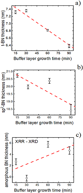
Figure 6. Thickness variation of the (a) turbostratic (b) sp2-BN (b) and (c) amorphous parts as a function of the growth time of the CFG buffer layer.
Download figure:
Standard image High-resolution imageThe obtained FTIR spectra (figure S9) were analysed within Dynamic Dielectric Function approximation taking into account the dielectric function of the h-BN layer [31, 39] and sapphire substrate [40, 41] through the calculation of reflectivity of the dielectric layer of thickness L on an infinite substrate. The fitted parameters were: energy and broadening of the E1u(TO) phonon in h-BN and the layer thickness. As seen in table 2 the thickness of the layers estimated from FTIR measurements correlates very well with those obtained from XRR assessments. Although one have to note that FTIR thickness estimates are systematically lower than the XRR estimates, particularly for the SII sample. We ascribe this difference to the presence of the amorphous part of the BN layer (table S2) which may pose a problem in the modelling of the FTIR measurements (figure S9).
3.4.2. High resolution x-ray diffraction
We have also performed x-ray diffraction experiments in the high resolution mode with x-ray optics involving Hart–Bartels type incident beam monochromator and analyser in front of the x-ray counter. Figure 7 shows results for sample S30 were we obtained signals from 0002/0003 h-BN/r-BN as well as 0004/0006 h-BN/r-BN structures. One has to remember that higher order reflections are very weak but can deliver significant information if recorded. As follows from JCPDF records for h-BN and r-BN [35], the intensity ratio 0002/0004 for h-BN is 100/6 and 0003/0006 ratio for r-BN is 100/4. If the recorded signal is measurable one can attempt to estimate such a x-ray reflection intensity ratio.
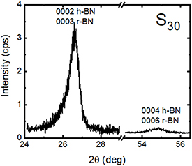
Figure 7. HRXRD diffraction results for 0002/0003 and 0004/0006 reflections of the h-BN and r-BN species (sample S30).
Download figure:
Standard image High-resolution imageWe have fitted the scan of sample S30 with a single Gaussian function in the case of 0004/0006 reflections and two Gaussians for the 0002/0003 part, since it may also include t-BN diffracted intensity (figure S4). The asymmetric distribution of the intensity for the 0002/0003 reflection can be safely attributed to the turbostratic stacking of the BN layer which cannot be seen for the 0004/0006 reflection. The fitted Gaussians were employed to estimate an intensity ratio of both distributions and it was found to be about 18.7. The JCPDF ratio value gives 16.67 for h-BN case. Since 0003/0006 r-BN is in the range of 25 one can conclude that most of the sp2-BN layer is h-BN with AA' stacking. There is probably a r-BN contribution in the grown layer, which can be expected and attributed to stacking faults of the structure, since the intensity ratio is slightly larger than expected for pure h-BN. Such a structure was already observed and reported [27] on sapphire substrate grown sp2-BN.
3.5. Uniformity of the sp2-BN across the wafer
We have chosen sample S30 as the best in our study from the point of view of uniformity across the whole 2' wafer. XRD (figure S5) and Raman measurements were taken along the diameter of the wafer and results are summarized in table 3. Since the footprint of the x-ray beam on the sample is in the range of 2 mm × 5 mm, meaning that the results average over macro size area, we have implemented Raman scattering mapping (figure S6) over areas 5 µm × 5 µm. The obtained averaged results are shown in table 3 and the specific areas A,B,C and D positions as indicated in figure 8.

Figure 8. Optical image of the whole wafer showing areas where the x-ray and Raman measurements were taken.
Download figure:
Standard image High-resolution image
Table 3. Measured and calculated values of the d0002/0003 spacing, h-BN/r-BN part thickness, positions of the Raman shift and FWHM of the Raman shift for sample S30 taken across the whole wafer.
| Position on the | Interplanar spacing | Scherrer thickness | Position of Raman | FWHM of Raman |
|---|---|---|---|---|
| wafer (figure 8) | of h-BN/r-BN (Å) | XRD of h-BN/r-BN (nm) | shift/FTIR (cm−1) | shift/FTIR (cm−1) |
| A | 3.34 | 14.8 | 1367.42/ 1367.23 | 26.1/ 21.1 |
| B | 3.34 | 19.9 | 1367.58/ 1367.36 | 27.2/ 22.5 |
| C | 3.34 | 20.6 | 1367.60/ 1367.23 | 27.2/ 21.5 |
| D | 3.34 | 15.1 | 1367.54/ 1367.26 | 24.2/ 21.1 |
The values in table 3 show a high uniformity of the d spacing and Raman peak positions across the wafer. There are some variations as far as thickness of the sp2-BN is concerned which probably are connected with overall geometry of the MOVPE growth system especially susceptor and rotation axis of it. The FWHM of the Raman shift reflects the structural quality of the measured material—the wider the line, the more structural defects in the final sp2-BN. In this case this is also directly connected with the thickness of the material and the growth temperature in a specific position of the wafer on the susceptor.
4. Conclusions
We have proposed and investigated a semi-homoepitaxial approach to the growth of sp2-BN on sapphire substrates by the introduction of an initial CFG step before the final growth using the FME mode. The main objective was to investigate the influence of growth time of the CFG buffer on the overall structure of the final BN layer. As indicated by XRD and HRXRD experiments, the total thickness of the BN layer is made up of two main components; a turbostratic part (t-BN) and a well-crystallized h-BN (AA' stacking) part with some addition of r-BN (ABC stacking). We show that XRR in combination with XRD can discern the presence of an amorphous phase in the grown layer. Our approach shows that a CFG buffer with a growth time of 15–30 min can successfully hinder the emergence of the amorphous phase.
The amorphous phase as a separate sublayer was already investigated and was ascribed to the high growth temperature in the process by X Yang et al[ 28], and was clearly pinpointed to be at the sapphire/BN interface. Lowering the growth temperature by 30 °C–1300 °C and introduction of an intentional AlN layer resulted in a total removal of the unwanted phase. The authors also suggest that the amorphous phase is a result of decomposition of properly grown sp2-BN into amorphous state by prolonged high temperature of growth process later in the course of the process [28]. Our results, which use an additional buffer layer (CFG) show that the amorphous phase can be controlled by limiting the growth time of such a buffer (figure 6). The trends observed in figure 6 strongly suggest that the amorphous phase can in our case be ascribed to the decomposition of the initial sp2-BN and a subsequent recrystallization into a final amorphous layer. The process of recrystallization mostly concerns the material grown in the CFG phase. The longer the growth time of CFG buffer the thicker is the amorphous layer (figure 6(c)) and the thinner are the t-BN and h-BN phase layers (figures 6(a)–(b)). When using only the FME mode to grow the BN layer, one is lacking the additional control (apart from growth temperature) to suppress the amorphization as evidenced by the fact that the amorphous phase is also present even for growth temperatures below 1300° (see results for sample SII and SI+II in table S1 and table 1)
The surface morphology, as observed by SEM and AFM show the well-known wrinkle pattern. This wrinkle pattern is usually attributed to the post growth cooling of the sample [20, 21, 26] and is an unavoidable result of the growth by MOVPE. It is also an indication of a fully continuous layer, which is weakly attached to the substrate. There is a significant addition of so called 'debris' [17, 20] on top of the wrinkle pattern in the form of random volume particles with a size of around 2–20 nm. These particles can be attributed to secondary out-of-plane nucleation centres, the growth of which is probably initiated right from the beginning of the process. Nucleation of these centres can be minimalized and controlled by the introduction of the CFG buffer layer with a short growth time in the MOVPE process (see figure 1).
The analysis of the Raman and photoluminescence results show that the presence of a CFG buffer layer also generally influences the additional background observed in both cases. Since the background luminescence is connected to the presence of unintentional point-like defects or aggregates of defects, our approach opens up the way to the successful control mechanism of elimination of such defects. Our results do not show a clear dependence between the defect density and the thickness of the CFG layer, but a general significant lowering of the defect density is clearly established (figures 3–4).
Our results of the lattice spacing in the c direction of the hexagonal structure show for all samples that, despite the different CFG layer growth times, the subsequent FME process results in an almost perfect d002 lattice spacing very close to the value for perfect h-BN crystal lattices (table 2). Since the only difference between the sole FME and combined CFG + FME processes is the growth of a buffer layer we can conclude that an addition of the CFG buffer is responsible for the better value for the d002 lattice spacing (table 2). The only variation observed is a change of the thickness of final sp2-BN (figure 6(b)). The turbostratic (t-BN) phase shows a similar behaviour (figure 6(a)).
In our study, we have investigated a limited number of growth parameters to clearly distinguish the changes resulting from the introduction of the CFG buffer layer. The final FME process was intentionally kept similar for all samples. One of the crucial parameters of MOVPE growth is the growth temperature of the layer and the thermal stability of the whole process. As reported in table 1 we have been monitoring real growth temperature via direct measurements by the multipoint pyrometer. Sample S60, S90 and S30 show similar temperatures but sample SI+II and S15 have slightly different values. It might be the consequence of thermal gradients in the MOVPE system associated with the geometry of the growth chamber and position of the wafers on the susceptor. This problem needs further fine tuning.
Our HRXRD results, which indicate that the final sp2-BN layer is an almost uniform h-BN crystal, fully support the conclusion that the proposed growth scheme (CFG + FME) is a very promising novel way to grow high quality wafer-scale h-BN layers on sapphire substrates. Since the proposed semi-homoepitaxial approach is carried out in one growth run it also seems to be more cost effective and does not require preparation of the special templates beforehand. Moreover, we do not have to introduce additional elements like Al or Cu that could influence the properties of BN, but use only boron and nitrogen in our buffer. It is clear that more studies of such processes are necessary in order to fine tune the final results, but the clear improvement observed in this work holds great prospects for successful application of the so grown wafer-scale h-BN.
Acknowledgments
This work has been partially supported by the National Science Centre under Grant Nos. 2019/33/B/ST5/02766.
We would like to extend our most sincere acknowledgements to our late colleague Krzysztof Pakuła for his pioneering work which has laid the necessary foundations in boron nitride MOVPE growth at our department.
Conflicts of interest
There are no conflicts of interest to declare.