A Survey of Analog-to-Digital Converters for Operation under Radiation Environments


1
R&D Department, Arquimea Ingeniería SLU, 28918 Leganés, Spain
2
IPTC, ETSI Telecomunicación, Universidad Politécnica de Madrid, 28040 Madrid, Spain
*
Author to whom correspondence should be addressed.
†
Current address: Calle Margarita Salas 10, 28918 Leganés, Madrid, Spain.
Electronics 2020, 9(10), 1694; https://doi.org/10.3390/electronics9101694
Submission received: 7 September 2020
/
Revised: 1 October 2020
/
Accepted: 3 October 2020
/
Published: 15 October 2020
/
Corrected: 29 December 2023
(This article belongs to the Special Issue Extreme-Environment Electronics: Challenges and Solutions)
Abstract
:In this work, we analyze in depth multiple characteristic data of a representative population of radenv-ADCs (analog-to-digital converters able to operate under radiation). Selected ADCs behave without latch-up below 50 MeV·cm2/mg and are able to bear doses of ionizing radiation above 50 krad(Si). An exhaustive search of ADCs with radiation characterization data has been carried out throughout the literature. The obtained collection is analyzed and compared against the state of the art of scientific ADCs, which reached years ago the electrical performance that radenv-ADCs provide nowadays. In fact, for a given Nyquist sampling rate, radenv-ADCs require significantly more power to achieve lower effective resolution. The extracted performance patterns and conclusions from our study aim to serve as reference for new developments towards more efficient implementations. As tools for this purpose, we have conceived FOM and FOM, two new figures of merit to compare radenv-ADCs that consider electrical and radiation performance.
1. Introduction
Several high reliability applications such as HEP (high energy physics), avionics, defense and space demand ADCs operating in harsh radiation and extreme temperature environments [1,2]. The design, manufacture and test of these ADCs require additional considerations and steps that, added to their low volume market, increase their price compared to COTS (commercial off-the-shelf ADCs). Different fields of knowledge—solid-state and nuclear physics, manufacturing technologies, radiation hardening and mixed-signal design techniques, test methodologies, industry standards, etc.—have to be combined to achieve a successful design.
The lack of ADCs meeting at the same time demanding electrical performance and radiation hardness specifications allows the use of COTS for high reliability applications. Furthermore, COTS could also be convenient in low radiation environments or in applications allowing replacement of damaged parts. Therefore, many COTS have been characterized to predict their behavior under radiation [3,4,5]. In fact, using COTS could economize development time and cost; however, radiation characterization cannot be skipped and additional countermeasures at system level—shielding, redundancy, watch-dogs, etc.—could be required to avoid unacceptable system malfunctioning. In addition, different manufacturing lots could perform differently during TID (total ionizing dose) screening, making hard to predict the final cost of the qualification campaign of COTS. In any case, inserting advanced commercial electronics operating in radiation environments has become an industrial trend that aims to benefit from cutting-edge IC (integrated circuit) solutions together with ad-hoc radiation hardening techniques at system level. Our revision work takes COTS into consideration and analyses this subset also separately.
Technology scaling has allowed faster applications integrating more functionalities in a single chip; collaterally, sensitivity to radiation has also varied [6,7]. In fact, atmospheric radiation can affect deep-submicron CMOS (complementary metal-oxide semiconductor) ICs not only in-flight but also on land [8,9]. Fortunately, some modern ‘More Moore’ [10] process options—SOI-FinFET (silicon on insulator fin-shaped field effect transistor), UTBB-FDSOI (ultra-thin body and buried oxide combined with fully-depleted silicon on insulator), etc.—and materials—high- dielectrics, germanium or silicon-germanium p-channels, etc.—show enhanced resilience to radiation [11,12,13]. Recurrent ADCs in space applications are usually implemented with mature technologies due to their in-flight heritage and the wide voltage ranges handled by the integrated analog front-end. Nevertheless, recent space market trends like fleets of compact-size satellites based on SoC (system on-chip) ICs require new radenv-ADC IP-cores (intellectual property) with reduced area and power consumption that can only be achieved with modern technologies. New radenv-ADC developments can benefit from the analyses presented in our work, since it collects the key references to overcome.
Several FOMs (figures of merit) are defined in the literature to evaluate the efficiency of an ADC; many of them are collected in [14]. Unfortunately, parameters used to evaluate radiation performance of radenv-ADCs are not considered in these FOMs. Moreover, radiation-hardened ADCs require additional power to accomplish their radiation requirements, making unfair their comparison with unhardened devices. In Section 2.3, we propose new figures of merit to evaluate the efficiency of radenv-ADCs that consider not only their electrical performance but also their radiation characterization.
In this work, we extract patterns on conversion resolution, characteristic frequencies, radiation performance, power efficiency, architectures and manufacturing processes of radenv-ADCs. After an exhaustive search in the literature, we have gathered a collection of ADCs without degradation of electrical performance below 50 krad(Si) of TID and with a latch-up LET (linear energy transfer threshold) above 50 MeV· cm2/mg. We have collected for each ADC several performance data from data-sheets, scientific publications and radiation reports (specially data considered in [15], to allow the comparison with scientific ADCs). The main contributions of this study with regard to previous analyses [16,17,18,19,20] are the inclusion of transients and upsets, the comparison of electrical performance patterns with scientific ADCs, the analysis of the COTS subset and the definition of new FOMs considering radiation performance. The methodology of our work described in this paragraph is graphically schematized in Figure 1.
This article has been organized such that: Section 2 summarizes how ADCs are evaluated electrically under radiation and proposes new figures of merit; Section 3 presents the selected ADCs for analysis; Section 4 analyses the selection of radenv-ADCs and compares it with the state of the art of scientific ADCs; Section 5 explains how to take advantage of the previous analysis while designing radenv-ADCs; overall conclusions are drawn in Section 6.
2. Performance Evaluation
We have classified the parameters used for performance evaluation of radenv-ADCs into three categories. Firstly, we recall the standard parameters used to measure electrical performance. Secondly, we collect conventional parameters used to evaluate radiation performance. Unfortunately, the power efficiency is not considered within the parameters of this second category, which is the reason why we propose new figures of merit in the third category to evaluate the efficiency of radenv-ADCs.
2.1. Parameters Shared with COTS
ADC data-sheets usually include standard parameters—input signal bandwidth, digital output rate, resolution and power dissipation—accompanied with FOMs in quasi-static—DNL (differential non-linearity), INL (integral non-linearity), gain and offset errors—and dynamic—DR (dynamic range), ENOB (effective number of bits), SFDR (spurious-free dynamic range), SINAD (signal-to-noise and distortion), SNDR (signal-to-noise and distortion ratio), SNR (signal-to-noise ratio) and THD (total harmonic distortion)—operations. Other parameters of interest provided are the operational temperature range, the input full-scale and the required clock frequency and jitter. Physical implementation details (such as manufacturing process or silicon area) are usually hard to find due to their commercial sensitive nature.
Parameters presented in the data-sheet of a radenv-ADC could depend on the target application. For example, linearity is evaluated with ENOB in telecommunications while INL and DNL are preferred in video acquisition. In Section 3.2 we explain how we have overcome this inconvenience to established a common playground to compare radenv-ADCs.
2.2. Parameters to Evaluate Radiation Performance
Radiation effects are a vast topic [21,22] even particularized for ADCs; this section provides a condensed summary that should be sufficient to understand radiation data presented afterwards.
Radiation effects on electronic devices can be classified in two main categories: CE and SEE (cumulative and single event effects, respectively). CE, in turn, are classified as TID effects if they are caused by ionizing radiation, or as DD (displacement damage) if radiation is non-ionizing. On the other hand, SEE are discerned into destructive or non-destructive, and can also be referred as hard or soft errors, respectively.
The radiation characterization of an ADC is performed by measuring the threshold of the physical magnitude provoking each effect. However, it is not necessary to reach the threshold if it is below the environmental specifications of the target application; in that case, the maximum tested value is reported. Bearable non-destructive effects are characterized such that the degradation (in case of CE) and the statistical error rate SER (in case of non-destructive SEE) during operation can be extrapolated; for those effects, the threshold and the behavior above it are reported.
The performance under radiation of an ADC is bound to the technology and libraries of devices used to implement it; this information is critical to plan effectively the radiation test campaign of an ADC, where accelerated tests (with harsher radiation conditions than during operation) are required to predict its behavior throughout its lifetime in a reasonable time. Below in this section, we bind some radiation effects with recurrent devices used in ADCs’ implementations.
2.2.1. Cumulative Effects
Tests performed for measuring CE are characterized by the total dose reached before unacceptable performance degradation. In mature technologies, ionizing radiation (usually measured in krad(Si) by exposure to a 60Co source) mainly affects MOS (metal oxide semiconductor) devices, while non-ionizing radiation (measured with the fluence in particles/cm2) specially involves bipolar ones. Additionally, bipolar devices (even parasitic structures [23]) can be affected by ionizing radiation at low dose rate (≤10 mrad(Si)/s) [24,25,26], making also the dose rate an important parameter for TID tests. For some ‘More Moore’ processes with thinner gate oxide but using thick BOX (buried oxide), ionizing radiation can provoke a back-gate effect [27].
2.2.2. Single Event Effects
The characterization of an ADC for a particular non-destructive SEE—SEFI, SET or SEU (single event functional interrupt, transient or upset, respectively)—can be summarized with the limits of the resultant Weibull fit—the LET (measured in MeV·cm2/mg) and the saturation cross section (given in cm2/device)—. On the other hand, destructive SEE—SEB, SEDR, SEL or SESB (single event burnout, dielectric rupture, latch-up or snap-back, respectively)—are characterized only with the LET.
Sensibility to non-destructive SEE has varied with technology scaling, making the characterization of SEFI, SET and SEU already necessary in SEE tests fifteen years ago. In addition, upsets could be difficult to be discerned from registered transients; tests reports shall clearly define these events to avoid confusions. Furthermore, in ADCs with high conversion rates, a SET could spread out through several samples; if this occurs, only one event is counted but the length of the burst of samples is also reported.
In some cases, SEL and SESB can be mitigated to non-destructive SEE if over-current watchdogs are implemented in the power supply at system level. In other words, SEL and SESB could be turned from hard to soft errors with an opportune power cycling.
2.3. Proposed Figures of Merit
A popular FOM to evaluate the efficiency of an ADC was proposed in [16]; it combines its power dissipation P together with its Nyquist sampling rate and its effective number of quantization levels 2 in the formula:
where:
From Equation (1) it is deduced that the more efficient an ADC, the smaller its FOM. However, increasing wisely by design the power consumption of an ADC enhances its radiation tolerance. This assertion is based on the fact that higher biasing makes leakage currents due to TID and charge generated during transients less representative with regards to the affected internal analog signals; in addition, higher currents imply faster transient response and hence shorter recovery time from a SET. In fact, from a performance under radiation point of view:
- The higher irradiated dose an ADC can stand without performance degradation, the robuster against radiation the ADC is.
- The more energized a particle shall be to cause an event in an ADC, the robuster against radiation the ADC is.
- The smaller the area an ADC has where a particle impact can affect its performance, the less sensitive to radiation the ADC is.
These trade-offs flow into the FOMs that we propose in Equations (3) and (4), which aim to evaluate the efficiency of an ADC operating under radiation:
where FOM is given by Equation (1), TID is the maximum ionizing dose without performance degradation and the other two parameters, LET and , are the characteristic limits of the Weibull fit for a particular SET definition.
Regarding units, FOM is given in joules per quantization level, TID in rads or Grays, LET in MeV·cm2/mg, in cm2/device and both FOM and FOM in quantization levels per milligram (levels/mg). Note that some minor unit conversions are required to obtain the proper values of FOM and FOM. It is deduced from Equation (3) that the more efficient an ADC is against TID, the bigger its FOM; comparably, a similar conclusion can be extracted from Equation (4): the more efficient an ADC is against SET, the bigger its FOM.
Fine tuning of the proposed figures may be accomplished by the exponentiation of the parameters on the right side of Equations (3) and (4), depending on the importance that the analyst wants to give to each parameter. Following the general formula for ADCs’ figures of merit presented in [14], the exponents of the bases FOM, TID, LET and are respectively −1, 1, 1 and −1 in Equations (3) and (4). For example, FOM can be customized having TID to the power of 2, if more emphasis to radiation performance is targeted evaluating the efficiency of the ADCs under analysis.
Furthermore, as will be shown in Section 4.3, the proposed figures of merit can be used to estimate which design solutions are more efficient considering their performance under radiation.
3. Inventory
3.1. Selection Criteria
We have surveyed and assessed the ADCs among the catalog of the leading suppliers to the space market—Analog Devices, Atmel, Cobham Gaisler, ST Microelectronics, Teledyne e2V, Texas Instruments, etc.—and among the more relevant publications about radiation effects on components—2010–2019 NSREC/REDW’s (and previous publications considered relevant) and all AMICSA’s and RADECS’ proceedings—. Candidates with degradation of electrical performance below 50 krad(Si) of TID or with a LET for latch-up below 50 MeV· cm2/mg were discarded. It is important to remark that neither all qualified ADCs are compliant with these two requirements nor, just because an ADC is not qualified, it is non-compliant. In fact, several EMs (engineering models) and COTS were included in the assessment.
3.2. Collected Data
Selected ADCs target different applications with different key parameters: high linearity and resolution are mandatory in video acquisition, while larger bandwidths are prioritized in telecommunications. However, while comparing two radenv-ADCs for a particular application, secondary parameters could become critical when the key ones are similar. It is hence important to establish a common playground to compare selected ADCs, as we explain below.
We have collected performance data and additional information from data-sheets [28,29,30,31,32,33] (both commercial and SMD formats), radiation reports [1,3,4,34,35,36,37,38,39] and scientific publications [20,40,41,42,43,44,45,46,47,48,49,50,51,52,53,54,55,56,57,58,59,60,61,62]. We have considered a total of 22 fields for each ADC: power consumption P, differential and integral non-linearities DNL/INL, effective number of bits ENOB, Nyquist sampling rate , input Nyquist bandwidth , FOM, FOM for low and high dose rates, FOM for transients and upsets, operational temperature range (T range), TID for low and high dose rates LDR/HDR, LET for latch-up events, Weibull curve limits for transients and upsets, SEE test method, technology and architecture.
Electrical performance data (P, INL, DNL and ENOB) were collected at nominal operation (nominal bias and sampling rate at 25 °C). Power consumption data from data-sheets were limited to single core information (excluding IO cells, other ADC cores inside the same chip, additional functionalities, etc.) to enable comparison with scientific publications that usually refer to single core data. ENOB was considered for the best case frequency inside the first Nyquist band. For few cases (AD7712S, RHD5940, RHD5950, RHD5958, ADS1258 and VASP), neither the SNDR nor the ENOB could be found. Therefore, the ENOB (needed for FOM calculation) had to be inferred from their declared number of bits NB and DNL or INL (expressed in LSBs) with the formula:
Since the actual ENOB comes from a dynamic measure, it would always be close but below the inferred ENOB (that comes from a quasi-static measure).
Since it is hard to discern SETs from SEUs during SEE tests of an ADC, radiation data were collected and classified as originally reported. In case that multiple data are available, the worst case is considered.
3.3. Selected ADCs for Analysis
To increase the number of samples under analysis, few exceptions were made for both requirements described in Section 3.1:
- TID requirement was relaxed for a few ADCs with characterization data for transients and upsets (AD7712, MAX145, ADS1258, LTC1419, AD7984, ADS5483 and ADS5444-SP).
- Three TID compliant ADCs for which no SEE data could be found in the literature were exempt from the latch-up requirement (AD570S, AD9254S and TS8388B).
Finally, fifty four ADCs were selected for the analysis; their collected data are presented in Table 1. For a better understanding of the table, the following explanations shall be considered:
- The table’s header is divided into four lines: ‘Group’ (uppermost line), ‘Sub-group’ (second uppermost line), ‘Field’ (second lowermost line) and ‘Units’ (lowermost line).
- Each of the 22 fields described in Section 3.2 is represented in one column of the table.
- The 22 fields are classified in tree different groups: ‘Performance’, ‘Hi-Rel’, and ‘Additional Information’.
- Fields conceptually related and/or sharing the same units in the ‘Performance’ and ‘Hi-Rel’ groups are gathered in the same sub-group.
- Collected data are presented in the table’s body, below the table’s header. Empty boxes therein (fulfilled with symbol “-”) are non-available data due to lack of information in the literature.
- The leftmost column of the table’s body collects the names of the selected radenv-ADCs. Particularly, COTS are marked with a double asterisk (**) after their name.
- The ‘FOM’ sub-group within the ‘Performance’ group is composed by the FOMs described in Section 2.3. Columns ‘W’, ‘TID(L)’, ‘TID(H)’, ‘SET’ and ‘SEU’ of this sub-group collect respectively for the selected radenv-ADCs their FOM, their FOM for TID measured at low and/or high dose rates, and their FOM for transients and/or upsets characterization.
- In the ‘ENOB’ column, inferred data using Equation (5) are marked with a single asterisk (*). Additionally, in the ‘FOM’ sub-group columns, data calculated using an inferred ENOB are also marked with a single asterisk (*).
- In the ‘Hi-Rel’ group, TID, LET and measurements are gathered respectively in the ‘TID’, ‘LET’ and ‘’ sub-groups. TID measurements are discerned in two columns (‘LDR’ or ‘HDR’) depending on the dose rate as defined in Section 2.2.1. On the other hand, LET and measurements are segregated in different columns depending on the nature of the SEE (‘SEL’, ‘SET’, or ‘SEU’ columns for latch-up, transients or upsets respectively). As explained in the first paragraph of Section 2.2.2, SEL measurements only consider the LET.
- Acronyms used in the ‘SEE test’ column are listed in Table 2.
- The ‘Tech.’ column collects manufacturing process details extracted from the literature. This information could be: the process type (bipolar, complementary-bipolar, CMOS, linear compatible CMOS, bipolar-CMOS, etc.), the process name (B7HF200, BiCom3, BiCom3X, BiCMOS9, C021.A, CMOS9, CMOS9X, XFCB, XH035, etc.), or the CMOS node (350 nm, 250 nm, 180 nm, 130 nm, 32 nm, etc.). Additional technological explanations are provided in Section 4.4.
- Acronyms used for the different ADC architectures in the ‘Arc.’ column are listed in the first sentence of Section 4.5.
4. Data Analysis
As advanced in Figure 1, the selection described in Section 3 is analyzed and compared with designs presented at the IEEE ISSCC (International Solid-State Circuits Conference) and the VLSI (Symposia on Very Large Scale Integration Technology and Circuits) from 1997 to 2019. These designs are considered the state of the art of scientific ADCs in this analysis. From now on in this section, the former population of ADCs is referred as the selection and the latter as the state of the art.
The presented analysis aims to extract patterns of the power efficiency of radenv-ADCs. Unfortunately, it cannot be warrantied that all collected data were measured with the same criteria; consequently data presented in Table 1 could be slightly shifted. This is specially critical for radiation data, as will be explained in Section 4.3. However, this fact will have little impact on the final conclusions about patterns and performance envelopes of radenv-ADCs.
Data from Table 1 are represented in several ways in Figure 2, Figure 3, Figure 4, Figure 5, Figure 6, Figure 7 and Figure 8 to extract different patterns of the selection; the envelope defined by the best performing specimens is depicted with a dashed line in each figure. Additionally, the envelope defined by the best performing specimens of the state of the art is represented with a solid line in Figure 2, Figure 3, Figure 4 and Figure 5. Detailed data about each specimen and envelope of the state of the art can be found in [15]. Furthermore, we have discerned data by ADC architecture using different symbols (cf. legends).
Figure 2, Figure 3 and Figure 5 present envelopes shaped alike for both the selection and the state of the art; the same behavior is observed in Figure 4 up to 100 MHz. These facts endorse the assumptions that patterns between both populations can be compared and that conclusions from this comparison can be extracted considering that the main difference between both populations is the radiation hardening feature.
Inferred data in Figure 2, Figure 3, Figure 4 and Figure 5, Figure 7 and Figure 8 are marked with a black round circle around their symbolic representation. Since inferences could be slightly improved with regard to measures, the former are not considered to establish the envelopes in those figures. In any case, only one case with inferred data (ADS1258) is close to the envelopes.
4.1. Frequency and Resolution
Nyquist sampling rate and input bandwidth were selected as reference frequencies to establish a common playground for the whole selection. The choice of the latter is in detriment of some ADCs with a passband wider than their Nyquist input bandwidth; however, the best SNDR is usually obtained within the Nyquist input bandwidth, which justifies its choice.
Figure 2 depicts the ENOB of each selection’s member versus its Nyquist sampling rate . Their ceiling is 20.5 bits up to 1 kHz, decaying 1.5 bits per decade from this point (dashed line with interleaved crosses in Figure 2). Unfortunately, no TID data could be found in the literature for specimens supporting that ceiling (AD7984 and ADS5483). We have hence considered a more accurate envelope; it has the same slope from 10 kHz, but shifted 1 bit down (dashed line in Figure 2). The ceiling of the the state of the art is 20 bits up to 10 kHz and decays from this point 1.5 bits per decade. Comparing both envelopes, it can be said that radiation hardening does not affect the maximum achievable ENOB up to 1 kHz; nevertheless, ENOB is punished with 2 bits above 10 kHz. For both the selection and the state of the art, ENOB decays 1.5 bits per decade above 10 kHz. Furthermore, if data of the state of the art after 2008 were not considered, both envelopes would be overlapped. In other words, for a given , the best scientific ADCs back in 2008 already achieved the ENOB that the best available radenv-ADCs do nowadays.
In addition to the intrinsic limitations of ADCs—quantization noise, input-referred circuit noise, aperture uncertainty and comparators ambiguity—, radenv-ADCs are also limited in speed by the qualified packaging technologies [63]. This explains the sparsely populated area in Figure 2 for radenv-ADCs above 1 GHz and 10 bits compared to the the state of the art. Furthermore, our study has limited the collected data to single core solutions, while ADCs operating above 1 GHz are usually implemented with time-interleaved multi-core architectures.
Figure 3 plots the Nyquist input bandwidth against maximum SNDR for the selection’s members. It also includes the performance of an ideal sampler with sinusoidal input for two jitter cases of its sampling clock: solid and dashed lines represent 0.1 and 1 ps cases respectively. For a given ENOB, selection’s members with the highest bandwidth perform as ideal samplers with a sampling aperture uncertainty close to 1 ps. Jitter becomes more critical for bandwidths close to 100 MHz and above, for which the most performing selection’s members exceed the 1 ps line but without surpassing the 0.1 ps one. A practical conclusion at system level is that hi-rel TID tolerant oscillators shall provide a sampling clock better than 0.1 ps to avoid jitter limiting the performance of new radenv-ADC designs; this requirement can also be extended to PLLs in SoC implementations. Note indeed that this is a best case figure based on the comparison with a simplified mathematical model; jitter can be more harmful in the actual performance of an ADC depending on implementation particularities of each design. Jitter requirements for the state of the art are just above the 0.1 ps line (less than one order of magnitude above the selection’s). In fact, for the state of the art, jitter becomes more critical for bandwidths close to 1 GHz and above, for which the most performing members exceed the 0.1 ps line. In addition, if data after 2012 of the state of the art were not considered, its envelope in Figure 3 would be similar to the one of the selection. In other words, for a given SNDR, best scientific ADCs back in 2012 already achieved the input bandwidth that the best available radenv-ADCs do nowadays.
4.2. Power Efficiency
Differences between the selection and the state of the art are even more evident when power consumption is considered. Figure 4 represents FOM of each selection’s member against their Nyquist sampling rate ; on the other hand, Figure 5 portrays their power consumption over against their peak SNDR. In both figures, the slashed line stands for the selection’s bottom line (831 fJ/level) while the solid line does for the state of the art’s (0.89 fJ/level up to 100 MHz). Almost three orders of magnitude separate both lines in favor of the state of the art. Again, one specimen without TID data (AD7984) is excluded to determine the selection’s envelope. In both Figure 4 and Figure 5, selection’s and state of the art’s envelopes would match if data after 2002 of the state of the art were not considered. Put another way, best scientific ADCs back in 2002 already achieved the FOM that the best available radenv-ADCs achieve nowadays.
From Section 4.1 it was concluded that, for a given above 10 kHz, the best ENOB achievable for the selection is 2 bits below the state of the art’s. Additionally, Figure 4 shows that, for a given below 100 MHz, the best FOM achievable for the selection is more than 933 times (831/0.89) the state of the art’s. Using this information in Equation (1), we can extract that, for a given between 10 kHz and 100 MHz, the selection requires at least 233 times more power to achieve an ENOB at least 2 bits lower, in regard to the best members of the state of the art.
Radiation hardening entails additional power consumption. Bias currents are not optimized to enhance radiation tolerance. In addition, a design can be hardened including specific ad hoc blocks, which entail additional area and power. Furthermore, performance under radiation can be enhanced increasing the separation between devices and reducing the impedance to ground of critical nodes; both techniques increase circuit parasites and hence power consumption.
In mature CMOS technologies (180 nm nodes and above), the minimum width of ELT devices (enclosed layout transistors, used to mitigate TID effects), is several times the width of regular transistors, which also scale the design into a more power hungry one. From the digital circuitry point of view, hardened cells can consume twice power and be two to four times bigger than cells with the same functionality and speed from a commercial library [64].
4.3. Radiation Performance
TID is usually measured up to a predefined dose that can be lower than the maximum bearable before performance degradation. Something similar occurs with SEL characterization, where the maximum LET tested does not necessarily provoke latch-up events. SET and SEU tests have several degrees of freedom—test method, event detection criteria, sampling frequency, bias conditions, etc.—that make each ADC characterization very specific. In Table 2, we have listed the nine test methods used in the literature to evaluate the soft-error sensibility of radenv-ADCs; methods known by two different names are presented in the same line. Identified test methods for the selection are collected in column ‘SEE Test’ of Table 1. Unfortunately, different test methods used for the same ADC give similar SET LET but different SET cross-sections (even if within the same order of magnitude) [3,34,35,37,65]. In addition, SET/SEU cross-sections can depend on the sampling frequency of the ADC under test [34] and on the ionizing dose [5,66]. Therefore, comparing radiation performance across devices shall be accomplished carefully. This variability in test complicates the extraction of patterns on radiation performance. FOM and FOM can be used as a first filter to compare performance, but a closer look is required when figures are close.
Figure 6 plots the reported TID against nominal power consumption for each selection’s member. As expected, the best performing ADCs (slashed line), present greater TIDs for higher nominal power consumptions. However, power consumption is also related with other ADC parameters; the most important ones are included in FOM ( and ENOB). Since FOM combines TID with FOM, it can be used to evaluate the efficiency of an ADC including its TID performance. Figure 7 represents the calculated FOM against nominal power consumption for each selection’s member. Just Boeing-1 ADC [50,51] with levels/mg surpasses the selection’s envelope (slashed line), established in levels/mg by the rest of the best performing ADCs. This ADC is analyzed with other particular cases in Section 4.7.
The fact that FOM’s envelope is constant across for the selection (see Figure 4) could help to extract patterns about , and hence FOM, across . SET and SEU data were both used to calculate FOM due to the common physical phenomenon producing both effects. It is expected for both transients and upsets that LET and envelopes increase with P and respectively. Even if the selection seems to behave so, the limited number of selection’s members characterized in transients and/or upsets does not allow to extract clear patterns about these effects.
Figure 8 plots the calculated FOM for both SET and SEU against the nominal power consumption for each selection’s member. Also in this scenario, Boeing-1 ADC clearly outperforms the rest of the selection: its FOM ( levels/mg) is around two orders of magnitude above the second best value: levels/mg obtained by AD9246S. In a closer look to these two best values, both have similar FOM but the radiation performance of Boeing-1 ADC is clearly better than those of AD9246S (LE: 30.9 > 10 MeV·cm2/mg, : < cm2/device). Considering only upsets, the best FOM is obtained by ADC128S102QML-SP with levels/mg; its good performance is not only due to a good FOM (second best with 831 fJ/level), but also to a reduced ( cm2/device).
Since Boeing-1 has both the best FOM and the best FOM (both several times better than the second classified), we can conclude that it is the most power efficient randenv-ADC of the selection.
4.4. Technologies
Bipolar, CB (complementary-bipolar), LC2MOS (linear compatible CMOS), BiCMOS (bipolar-CMOS) and pure CMOS processes [75,76,77] are found among the selection (cf. column ‘Tech.’ in Table 1). Particularly, MOS processes have characteristic lengths of 0.35 μm, 250 nm, 180 nm, 130 nm, 90 nm, 65 nm and 32 nm, being 0.35 μm and 180 nm the two more recurrent (with at least ten and eleven specimens, respectively). Both 0.35 μm and 180 nm MOS nodes are usually accompanied with other process options—BJTs (bipolar juntion transistors), additional thicker gate oxide, etc.—that allow to integrate in a monolithic solution a wide voltage range analog front-end together with the ADC.
The organization contributing the most to the selection is Texas Instruments (with 22 specimens). BiCom3 and CMOS9 are its most recurrent technologies within the selection (with at least six and seven specimens, respectively); both are briefly described below.
BiCom3 is a CB SiGe BiCMOS triple-metal technology on SOI [78]. It includes 5V NPN and PNP SiGe BJTs and isolated 3.3 V 0.35 μm CMOS devices. It offers several process options for faster BJTs (3X and 3Y options for 25 and 33 GHz, respectively), for high voltage applications (3XHV option, up to 36 V) and without SOI (3XL bulk option); however, only BiCom3 (basic) and BiCom3X options can be found within the selection. The technology can be considered latch-up free and ELDRS immune (enhanced low dose rate sensitivity), and has been tested up to 150 krad(Si) of TID (ADS5424-SP) and up to neutrons/cm2 of DDD (DD dose) (ADS5400-SP).
CMOS9 is a DGO (dual gate oxide) CMOS process using STI (shallow trench isolation) for inter-device isolation [23]. It provides 1.8 V and 3.3 V CMOS devices with, respectively, 180 nm and <400 nm minimum gate lengths, and 5 nm and <10 nm gate oxide thicknesses. The process is originally from National Semiconductor, derived from the TSMC’s 180 nm process (Taiwan Semiconductor Manufacturing Company). The technology can be considered ELDRS immune and has been tested up to 300 krad(Si) at LDR and HDR of TID (ADC08D1000).
Special mention is deserved by the 32 nm CMOS SOI technology by IBM used to implement the best FOM and FOM specimen: the Boeing-1 pipelined ADC [50]. Combined with on-chip calibration, the technology has shown practically no variation up to 1 Mrad(Si) of TID for this application. In addition to analog-to-digital conversion, the technology was also proven suitable for other high-speed applications (such as SerDes, PLL and DRAM) in heavy-ions environments.
Radiation hardening in ADC applications can be achieved with multiple technologies; several options are combined to achieve a versatile and power efficient design. RHBD (radiation hardening by design) techniques at physical level (additional contact rings, smart device distribution, etc.) and certain technology options (buried layers, trenches, etc.) are used to enhance radiation performance. The smallest MOS node (32 nm) used up to now for radenv-ADCs seems, not only the most suitable for a SoC solution, but also the most power + radiation efficient when combined with calibration; however, greater nodes (0.35 μm and 180 nm, including other technology options) offer the possibility to integrate a wide voltage range analog front-end without neglecting the power + radiation efficiency. In any case, we shall remark that the SOI feature is always present in the best performing specimens of the selection.
4.5. Architectures and Applications
Five architectures can be found among the selection: , SAR (successive approximation register), PIP (pipelined), F (flash), and FIF (folded interpolated flash). We have illustrated this diversity by discerning data by architecture in Figure 2, Figure 3, Figure 4, Figure 5, Figure 6, Figure 7 and Figure 8 (cf. legends). Additionally, we have denoted surmised architectures with a question mark in column ‘Arc.’ of Table 1. As a briefing, we have collected in Table 3 the number of specimens, the ranges of ENOB, and FOM, and the average FOM and FOM for each architecture. Flash was dismissed from Table 3, since only one specimen uses this architecture among the selection.
ADC architectures are similarly distributed along frequency and resolution either the target application operates under radiation or not: ADCs target low-frequencies high-resolution applications, SAR do low/medium-frequencies medium/high-resolution, PIP do medium/high-frequencies moderate-resolution, and FIF do high-frequencies low-resolution. Radiation hardening can be enhanced at the expense of area and power consumption by including additional blocks (triple redundancy, anti-glitches, anti-bubbles, SEL and/or SEFI watch-dogs, digital error correction, etc.). On the other hand, selecting specific circuit structures for the composing blocks of the randenv-ADC can also enhance its radiation performance without significant impact in area or power consumption (i.e., using auto zeroing comparators against SET). The PIP architecture presents the best and within the selection (cf. Table 3). In fact, PIP is the preferred architecture for hardened ADCs, with 21 specimens among the selection. SAR is also well represented, but it has more COTS among its population (7/19 versus 3/21 for PIP), and worst and .
Latency is a major concern for some ADC applications. As a rule of thumb, we can arrange architectures in the following order, from shorter to longer latency: flash < FIF < PIP < SAR <. Additionally, some ADC applications recur to down-sampling to extend the analogue bandwidth to be digitized; this technique has being lately the tendency in satellite communications where digital down-conversion of L- and S-bands signals relaxes the requirements of the RF front end. On the other hand, the inherent loop filter of architectures provides an intrinsic anti-aliasing feature that can save additional filtering stages at system level. In addition, the intrinsic oversampling feature of ADCs can be seen as a redundancy spread in time [79].
Considering the virtues and drawbacks of each architecture briefly discussed in this section, in Table 4 we have linked the more recurrent applications in radiation environments with their most suitable ADC architectures; a higher suitability is emphasized with a double check mark instead of a single one. We can consider SAR the most versatile architecture since it fits in almost all the considered applications.
Depending on the target application, some soft error test methods (cf. Table 2) could be more adequate than others. In Table 5, we present our recommendations according to the following criteria: test methods 1P or S are dismissed due to their reduced monitoring of output codes; QS is perfect for slow high-resolution applications; DAC method is discarded for long latency and/or very high resolution applications; the other test methods are similar, and can all fit for medium/high-speed applications.
4.6. COTS within the Selection
COTS are marked with a double asterisk (**) after their name in Table 1 (ADS1281, AD7712, AD7872T, MAX145, ADS1258, LTC1604, LTC1409, ADC124S101, AD7984, AD6640, ADS5483 and SPT7725); they are also easily recognizable therein since their temperature range is smaller than [−55; 125] °C. Two main reasons explain the presence of COTS in the selection: either they cover a range of sampling frequencies that hardened ADCs do not, or they offer a better FOM compared to their surrounding hardened counterparts.
If we consider the efficiency including TID performance, COTS are far from the envelopes in Figure 6 and Figure 7. On the other hand, even if the best performing COTS are far from the most efficient specimen in Figure 8 (Boeing-1 pipelined ADC), they present good FOM compared to other hardened ADCs. In other words, COTS could have shorter lifetime due to TID compared to hardened ADCs; however, since soft errors are almost impossible to be totally mitigated (even in hardened ADCs), COTS usage could be worthy in short lifetime applications, where the power consumption and/or the cost are prioritized. HEP (where data acquisition systems can be replaced) and fleets of small satellites (where the viability depends on the price per satellite) are de facto target applications for COTS.
4.7. Particular Cases
ADCs of the selection with outstanding efficiency under radiation are deeply analyzed below.
- AD7984: This COTS is a SAR ADC with the best FOM of the selection (122 fJ/level). It offers 16 ENOB sampling at 1.33 MS/s. No TID data were found in the literature, but its good electrical performance gives to this ADC a high FOM ( levels/mg). It also has a high SEL LET (106.2 MeV·cm2/mg).
- ADC128S102QML-SP: This qualified SAR ADC is implemented with a 0.35 μm CMOS process. Its 2.7 mW reduced power consumption together with its 11.7 ENOB at 1 MS/s give it a FOM of 0.8 pJ/level. Its good FOM combined with its performance under radiation give it the best FOM for SEU ( levels/mg). It also has a high FOM ( levels/mg for both LDR and HDR) and SEL LET (121.8 MeV·cm2/mg).
- Boeing-1: This pipelined ADC is implemented with a 32 nm CMOS SOI process. Its high 200 MS/s sampling rate together with its 7.4 ENOB and 39 mW power consumption give it a FOM of 1.1 pJ/level. It performs exceptionally good under radiation (mainly due to its calibration features and the technology used for its implementation) which, combined with a good FOM, results in the best FOM and FOM within the selection ( and levels/mg, respectively). It also offers the best SEL LET (170 MeV·cm2/mg).
5. Design Guidelines
From the analysis presented in Section 4, we have extracted several recommendations for the circuit design of radenv-ADCs. We have distributed these advises along the following simplified 5-step design flow:
- Step 1—Analysis of the target application and the available solutions
- Step 2—Selection of the manufacturing technology
- Step 3—Selection of the ADC architecture
- Step 4—Circuit design
- Step 5—Design validation
For a better understanding, before describing each step in Section 5.2,Section 5.3,Section 5.4,Section 5.5 and Section 5.6, we have summarized in Section 5.1 the overall radiation hardening strategy across the design flow.
5.1. Radiation Hardening Strategy
The hardening strategy against radiation effects mainly depends on the target application (Step 1) and the selected manufacturing technology (Step 2). Nevertheless, an optimum outcome is only possible when the strategy is tailored for the whole design flow. Below, we have broken down our proposal into a sequence of activities linked with the design steps (specified in parentheses):
- For mature applications, reference data are extracted from previous radenv-ADC solutions. (Step 1)
- Electrical and radiation requirements are specified based on the high-level requirements of the target application. (Step 1)
- Technologies and architectures in line with the specified requirements are noted down. (Step 1)
- Hardening-by-process options and hardening-by-design techniques are identified and analyzed for each considered technology. (Step 2)
- Technologies offering libraries of hardened cells and/or basic IP-cores are prioritized. (Step 2)
- As a result of the two previous activities, the manufacturing technology is selected from the preliminary options. (Step 2)
- Devices to be used in the design are chosen from the technology libraries. (Step 2)
- Needed rad-hard cells (but unavailable in the selected technology) are identified. (Step 2)
- Relying on the previous technological choices, the basic ADC architecture is selected from the preliminary options. Hardening blocks against SEFI (current alarms, watch-dogs, etc.), and test structures (test buses, built-in self tests, etc.) are included as part of the radenv-ADC architecture. (Step 3)
- Unhardened ADC designs with compatible requirements, implemented in the same technology, and with the same architecture, are compiled and analyzed. If plausible, one of them could be used as the starting point of the circuit design. (Step 4)
- Unavailable rad-hard cells are designed with a full-custom approach. (Step 4)
- Hardening-by-design techniques are applied at block-level. (Step 4)
- Electrical and radiation requirements are verified by simulation for the whole design. (Step 4)
- Electrical and radiation requirements are validated with test measurements. (Step 5)
Note that this hardening strategy can be adapted with minor changes to the design flow of other mixed-signal devices.
5.2. Step 1—Analysis of the Target Application and the Available Solutions
A good understanding of the target application is critical to effectively extract the functional (interfaces, communication protocols, operating modes, etc.), electrical (voltage levels, expected power consumption, etc.), mechanical (die and package dimensions, bond-pads dimension and position, bonding method, etc.), environmental (temperature range, performance under radiation, etc.), and reliability (lifetime, SER, etc.), requirements of the new radenv-ADC. Particularly, radiation and reliability requirements can be estimated using space environments software, models, and tools, such as CRÈME [80,81], FASTRAD [82], GEANT4 [83,84], OMERE [85], etc. Furthermore, previous solutions (i.e., data collected in Table 1) and/or cutting-edge technologies can inspire particular requirements and other design features (such as the manufacturing technology and the ADC architecture).
For novel applications, new radenv-ADCs are developed to fulfill key requirements that available radenv-ADCs cannot fulfill. On the other hand, for mature applications, new developments usually enhance important parameters that were considered secondary in early stages of the application’s life cycle. A good example illustrating both cases is the power consumption of radenv-ADCs targeting digital down-conversion of L-band signals; this requirement has become more demanding over time to offer more competitive solutions. It is hence critical to identify in Step 1 which parameters should be prioritized above others, considering that the preferences could have changed over time for mature applications. This approach helps solving possible trade-off conflicts in later steps.
The recent industrial trend of compact-size satellite-fleets in LEO with reduced lifetime (5 to 7 years) relaxes the radiation requirements of radenv-ADCs targeting related applications. In fact, TID is smaller for shorter missions, and the exposure to solar particle events in LEO is reduced compared to higher orbits. Collaterally, this approach reduces power consumption and shielding requirements, and is hence consistent with the size and weight reduction of the overall satellite.
The most important outcomes of Step 1 are the requirements specification, and the preliminary options of manufacturing technologies and ADC architectures that are suitable for the new design.
5.3. Step 2—Selection of the Manufacturing Technology
In this step, the best technology for the implementation of the new radenv-ADC is identified. The options were limited in Step 1 to those in line with the application requirements. For example, a low-voltage technology could be incompatible with the monolithic implementation of a radenv-ADC requiring a wide voltage front-end. In fact, technologies without radiation characterization data are usually discarded, but those with latch-up immunity and minimum TID degradation are marked as preferential. Particularly, deep sub-micron CMOS nodes offering SOI-FinFET, UTBB-FDSOI [13], high- dielectrics, or devices with Ge or SiGe p-channel should be preferred [11,12]. For all the considered technologies, the following features should be analyzed:
- Inter-device isolation options—LOCOS (LOCal Oxidation of Silicon), STI, DTI (Shallow or Deep Trench Isolation), buried layers, SOI, etc.—to evaluate the SEL sensibility.
- TID degradation and possible countermeasures: ELT availability, transistors minimum aspect ratio to mitigate performance degradation, etc.
- Effective volume of the technology devices to calculate the collected charge at an ion strike for different energies (for SET simulations).
- Availability of rad-hard libraries and IP-cores.
The selected technology is the one offering the best trade-off between electrical performance, hardening capability, and manufacturing price (usually following this prioritized order for radenv-applications). After the technology’s choice, the process options (top-metal thickness, use of buried layers, etc.) and the technology devices to be used in the design are selected. Additionally, missing rad-hard cells considered important for the design are identified for their later implementation in Step 4.
5.4. Step 3—Selection of the ADC Architecture
Usually, after analyzing the radenv-ADC requirements in Step 1, no more than two possible architectures are considered. Traditionally, the preferred choice has been a PIP architecture, since it offers a good trade-off between electrical performance and radiation robustness (cf. Section 4.5). In fact, PIP achieves higher resolutions than F or FIF, and is easier to harden against SET than or SAR. However, PIP cannot reach the ENOB that does, or be as power efficient as modern SAR. In short, the architecture choice is highly dependent on the particular radenv-ADC requirements. As a rule of thumb, it is advisable to use architecture for low-frequencies high-resolution applications, SAR for low/medium-frequencies medium/high-resolution, PIP for medium/high-frequencies moderate-resolution, and FIF for high-frequencies low-resolution.
Once the basic ADC architecture is chosen, the need of additional hardening blocks against SEFI (current alarms, watch-dogs, etc.) is evaluated with system-level simulation. Additionally, test structures (test buses, built-in self tests, etc.) to be included are also assessed.
5.5. Step 4—Circuit Design
Intuitively, it makes sense to start a new radenv-ADC from a previous unhardened design with good electrical performance. However, the hardening task may be impractical if important radiation hardening considerations were overlooked in the original design. For example, for technologies requiring the replacement of the planar transistors by ELTs [86,87] (to avoid excessive performance degradation caused by TID), it must be checked that the original design does not have planar transistors narrower than the minimum width required by ELTs (W 3·W). Something similar occurs for the node splitting technique [88] against SET (transistor width should allow being divided at least by two or four in the dual- and quad-paths hardening, respectively). The comparison between radenv-ADCs and scientific ADCs (cf. Section 4.1 and Section 4.2) gives an order of magnitude of what is reasonable to increase the power consumption to mitigate radiation effects (for a given between 10 kHz and 100 MHz, collected radenv-ADCs require at least 200 times more power to achieve an ENOB at least 2 bits lower than scientific ADCs). In any case, a new radenv-ADC can be designed from scratch, considering all the applicable hardening-by-design techniques from the beginning. To avoid unnecessary design effort, the unavailable rad-hard cells identified in Step 4 are designed with advanced TCAD (Technology Computer-Aided Design) tools once it is required to integrate them in the circuit. Furthermore, to avoid unnecessary power consumption, it is strongly recommendable to tailor the hardening effort for each particular design case: not all nodes are critical, and some of them can be SET hardened with a capacitance to ground (DC biased nodes, for example). A good approach to detect SET sensitive nodes is by analyzing the effects of injecting calibrated current pulses [89] throughout the circuit in different moments of a transient simulation [90,91].
5.6. Step 5—Design Validation
The test conditions for the soft error characterization of the developed radenv-ADC shall emulate the target application as much as possible. Considering the features of each soft error test method, QS better fits with low-speed high-resolution applications, and CS with the rest.
6. Conclusions
After an exhaustive search in the literature, we have analyzed a collection of radenv-ADCs able to bear TID above 50 krad(Si) and without latch-up below 50 MeV·cm2/mg regarding resolution, characteristic frequencies, power efficiency, radiation performance, manufacturing technologies, circuit architectures, and possible applications. Furthermore, we have also exposed remarks about its COTS sub-population and other particular cases. For the analyses only relying on electrical parameters, we have compared the extracted patterns with those of scientific ADCs. In this comparison, we have extracted that, for a given between 10 kHz and 100 MHz, collected radenv-ADCs require at least 200 times more power to achieve an ENOB at least 2 bits lower than scientific ADCs.
In this survey, we have discerned up to nine different test methods to characterize the soft errors of an ADC under heavy ions; two of them can be considered obsolete because of the scarce output codes monitored. Unfortunately, radiation performance is not consistent among different test methods for the same ADC, which complicates the comparison between ADCs characterized with different test methods. In any case, RHBD was proven to be effective in almost all CMOS technology nodes from 350 nm down to 32 nm; particularly, the SOI feature can be considered a mandatory technology option to achieve an optimum radiation performance. Regarding ADC architectures, we have confirmed that pipeline is the most recurrent among hardened ADCs; however, we have considered SAR the most versatile, since it is suitable for the vast majority of applications in radiation environments. We have pointed out that systems engineers recur to COTS looking for specific sampling frequencies or higher electrical performance uncovered by hardened ADCs. However, radiation characterization of COTS cannot be skipped and additional countermeasures could be required to avoid unacceptable system malfunctioning. Furthermore, we have defined FOM and FOM, two new figures of merit that evaluate the efficiency of radenv-ADCs considering electrical and radiation performance. These FOMs were used as a first approximation to orient many of our analyses; however, a closer look to the appropriate specific data is required afterwards to extract accurate conclusions about radenv-ADCs.
Finally, based on the analyses that we have presented before, we have recommended some guidelines for circuit designers interested in the development of radenv-ADCs.
Author Contributions
This work was mainly accomplished by E.P.-G. (conceptualization, investigation, methodology, data curation, formal analysis, project administration, resources, software, visualization and original draft preparation) and was participated with the key contribution of M.L.-V. (conceptualization, supervision, validation, manuscript review & edition and funding acquisition). All authors have read and agreed to the published version of the manuscript.
Funding
Marisa López-Vallejo was partly funded by the NEUROWARE project (PGC2018-097339) from the Spanish Ministry of Science and Innovation.
Acknowledgments
We want to thank David Levacq from the Electrical Engineering Department (TEC-EDM) of ESA-ESTEC for referring us to [55].
Conflicts of Interest
The authors declare no conflict of interest.
Abbreviations
The following abbreviations are used in this manuscript:
| 1P | Single-Point (SEE test method) |
| 4P | Four-Points (SEE test method) |
| ADC | Analog-to-Digital Converter |
| AMICSA | (International Workshop on) Analogue and Mixed-Signal Integrated Circuit for Space Applications |
| BF | Beat Frequency (SEE test method) |
| BiCMOS | Bipolar CMOS |
| BJT | Bipolar Junction Transistor |
| BOX | Buried Oxide |
| CER | Code Error Rate (SEE test method) |
| COTS | Commercial Off-The-Shelf (ADCs) |
| CMG | Control Moment Gyroscope |
| CMOS | Complementary Metal-Oxide Semiconductor |
| CS | Coherent Sampling (SEE test method) |
| DAC | Digital-to-Analog Converter |
| DC | Direct Current |
| DD | Displacement Damage |
| DDC | Digital Down-Converter |
| DDD | DD Dose |
| DGO | Dual Gate Oxide |
| DIS | Dynamic Input Signal (SEE test method) |
| DNL | Differential Non-Linearity |
| DOI | Digital Object Identifier |
| DR | Dynamic Range |
| DS or | Delta-Sigma (ADC architecture) |
| DT | Dynamic Threshold (SEE test method) |
| DTI | Deep Trench Isolation |
| ELDRS | Enhanced Low Dose Rate Sensitivity |
| ELT | Enclosed Layout Transistor |
| EM | Engineering Model |
| ENOB | Effective Number Of Bits |
| ESA | European Space Agency |
| F | Flash (ADC architecture) |
| FDSOI | Fully Depleted Silicon On Insulator |
| FIF | Folded-Interpolated Flash (ADC architecture) |
| FinFET | Fin-shaped Field Effect Transistor |
| FOM | Figure Of Merit |
| GNSS | Global Navigation Satellite Systems |
| HDR | High Dose Rate |
| HEP | High Energy Physics |
| IC | Integrated Circuit |
| IEEE | Institute of Electrical and Electronics Engineers |
| INL | Integral Non-Linearity |
| IP-core | Intellectual Property core |
| ISSCC | International Solid-State Circuit Conference |
| LC2MOS | Linear Compatible CMOS |
| LDR | Low Dose Rate |
| LEO | Low Earth Orbit |
| LET | Linear Energy Transfer Threshold |
| LOCOS | LOCal Oxidation of Silicon |
| LSB | Least Significant Bit |
| MDPI | Multidisciplinary Digital Publishing Institute |
| MOS | Metal-Oxide Semiconductor |
| NASA | National Aeronautics and Space Administration (USA) |
| NB | Number of Bits |
| NSREC | Nuclear and Space Radiation Effects Conference |
| P | Power (consumption) |
| PIP | Pipelined (ADC architecture) |
| PLL | Phase-Locked Loop |
| QS | Quasi-Static (SEE test method) |
| RADECS | (European Conference on) Radiation and its Effects on Components and Systems |
| radenv | (ADCs/applications operating in) Radiation Environments |
| rad-hard | Radiation Hardened |
| R&D | Research and Development |
| REDW | Radiation Effects Data Workshop |
| RF | Radio Frequency |
| S | Static (SEE test method) |
| SAR | Successive Approximation Register (ADC architecture) |
| SEB | Single Event Burnout |
| SEDR | Single Event Dielectric Rupture |
| SEE | Single Event Effect(s) |
| SEFI | Single Event Functional Interrupt |
| SEHE | Single Event Hard Error |
| SEL | Single Event Latch-up |
| SER | statistical error rate |
| SESB | Single Event Snap-Back |
| SET | Single Event Transient |
| SEU | Single Event Upset |
| SFDR | Spurious Free Dynamic Range |
| SINAD | Signal-to-Noise And Distortion (ratio) |
| SNDR | Signal-to-Noise and Distortion Ratio |
| SNR | Signal-to-Noise Ratio |
| SoC | System on-Chip |
| SOI | Silicon On Insulator |
| STI | Shallow Trench Isolation |
| TCAD | Technology Computer-Aided Design |
| THD | Total Harmonic Distortion |
| TID | Total Ionizing Dose |
| TSMC | Taiwan Semiconductor Manufacturing Company |
| USA | United States of America |
| UTBB | Ultra-Thin Body and BOX |
| VLSI | Very Large Scale Integration |
| VLSICS | VLSI Circuits Symposium |
References
- Kniffin, S.; Kim, H.S.; Palor, C. Single Event Effects Test Report for GSFC Test Trip to TAMU; Technical Report; NASA: Washington, DC, USA, 2003.
- Boccardi, A. Ongoing electronic development in the CERN Beam Instrumentation Group: Challenges and solutions for the measurement of particle accelerator beam parameters. J. Instrum. 2012, 17–21. [Google Scholar] [CrossRef]
- Berg, M.D.; Kim, H.S.; Phan, A.M. Heavy Ion SEE Tests for Texas Instruments ADS5483 ADC; Technical Report; Texas Instruments: Dallas, TX, USA, 2010. [Google Scholar]
- VonBergen, W.; Salzman, J.; Baumann, R.; Dahl, B. ADS5474: SEE Report; Technical Report; Texas Instruments: Dallas, TX, USA, 2013. [Google Scholar]
- Chen, K.; Chen, H.; Kierstead, J.; Takai, H.; Rescia, S.; Hu, X.; Xu, H.; Mead, J.; Lanni, F.; Minelli, M. Evaluation of commercial ADC radiation tolerance for accelerator experiments. J. Instrum. 2015, 10. [Google Scholar] [CrossRef]
- Srour, J.R.; Marshall, C.J.; Marshall, P.W. Review of displacement damage effects in silicon devices. IEEE Trans. Nucl. Sci. 2003, 50, 653–670. [Google Scholar] [CrossRef]
- Robert Ecoffet (CNES). In-flight anomalies on electronic devices. In Radiations Effects on Embedded Systems, 1st ed.; Velazco, R., Fouillat, P., Reis, R., Eds.; Springer: Dordrecht, The Netherlands, 2007; pp. 31–68. [Google Scholar] [CrossRef]
- Barth, J.L.; Dyer, C.S.; Stassinopoulos, E.G. Space, atmospheric, and terrestrial radiation environments. IEEE Trans. Nucl. Sci. 2003, 50, 466–482. [Google Scholar] [CrossRef]
- Hubert, G.; Artola, L.; Regis, D. Impact of scaling on the soft error sensitivity of bulk, FDSOI and FinFET technologies due to atmospheric radiation. Integr. VLSI J. 2015, 50, 39–47. [Google Scholar] [CrossRef]
- Allan, A.; Badaroglu, M.; Barnett, J.; Fukuzaki, Y.; Gargini, P.; Gottschalk, C.; Inoue, H.; Isobayashi, A.; Kahng, A.; Kim, S.; et al. More Moore; Technical Report; International Technology Roadmap for Semiconductors 2.0. 2015. Available online: https://www.semiconductors.org/wp-content/uploads/2018/06/5_2015-ITRS-2.0_More-Moore.pdf (accessed on 17 January 2020).
- Metcalfe, J.; Dorfan, D.E.; Grillo, A.A.; Jones, A.; Mendoza, M.; Rogers, M.; Sadrozinski, H.F.; Seiden, A.; Spencer, E.; Wilder, M.; et al. Evaluation of the radiation tolerance of SiGe heterojunction bipolar transistors under 24GeV proton exposure. IEEE Nucl. Sci. Symp. Conf. Rec. 2005, 2, 974–977. [Google Scholar] [CrossRef]
- Kulkarni, S.R.; Schrimpf, R.D.; Galloway, K.F.; Arora, R.; Claeys, C.; Simoen, E. Total ionizing dose effects on Ge pMOSFETs with high-k Gate Stack: On/Off Current Ratio. IEEE Trans. Nucl. Sci. 2009, 56, 1926–1930. [Google Scholar] [CrossRef]
- Roche, P.; Autran, J.L.; Gasiot, G.; Munteanu, D. Technology downscaling worsening radiation effects in bulk: SOI to the rescue. In Proceedings of the 2013 Technical Digest—International Electron Devices Meeting (IEDM), Washington, DC, USA, 9–11 December 2013. [Google Scholar] [CrossRef]
- Jonsson, B.E. Using figures of merit to evaluate measured A/D-converter performance. In Proceedings of the 2011 IMEKO IWADC & IEEE ADC Forum, Orvieto, Italy, 30 June–1 July 2011. [Google Scholar]
- Murmann, B. ADC Performance Survey 1997–2019; Stanford University: Stanford, CA, USA, 2019; Available online: http://web.stanford.edu/~murmann/adcsurvey.html (accessed on 18 January 2020).
- Walden, R.H. Analog-to-digital converter survey and analysis. IEEE J. Sel. Areas Commun. 1999, 17, 539–550. [Google Scholar] [CrossRef]
- Merkel, K.; Wilson, A. A survey of high performance analog-to-digital converters for defense space applications. In Proceedings of the 2003 IEEE Aerospace Conference Proceedings (Cat. No.03TH8652), Big Sky, MT, USA, 8–15 March 2003; Volume 5, pp. 2415–2427. [Google Scholar] [CrossRef]
- Murmann, B. A/D converter trends: Power dissipation, scaling and digitally assisted architectures. In Proceedings of the 2008 Custom Integrated Circuits Conference (CICC), San Jose, CA, USA, 21–24 September 2008; Volume 1, pp. 105–112. [Google Scholar] [CrossRef]
- Jonsson, B.E. A survey of A/D-Converter performance evolution. In Proceedings of the 2010 17th IEEE International Conference on Electronics, Circuits and Systems, Athens, Greece, 12–15 December 2010; pp. 766–769. [Google Scholar] [CrossRef]
- Irom, F.; Agarwal, S.G. Compendium of single-event latchup and total ionizing dose test results of commercial analog to digital converters. In Proceedings of the 2012 IEEE Radiation Effects Data Workshop, Miami, FL, USA, 16–20 July 2012; pp. 1–14. [Google Scholar] [CrossRef]
- Baumann, R.; Kruckmeyer, K. Radiation Handbook for Electronics; Texas Instruments: Dallas, TX, USA, 2019; p. 117. [Google Scholar]
- Paillet, P.; Fleetwood, D.M.; Rodbell, K.P.; Entrena, L.; Aguirre, M.; Campola, M. Short Course Notes; RADECS: Montpellier, France, 2019; p. 204. [Google Scholar]
- Kruckmeyer, K.; Prater, J.S.; Brown, B.; Trinh, T. Analysis of low dose rate effects on parasitic bipolar structures in CMOS processes for mixed-signal integrated circuits. IEEE Trans. Nucl. Sci. 2011, 58, 1023–1031. [Google Scholar] [CrossRef]
- Fleetwood, D.; Kosier, S.; Nowlin, R.; Schrimpf, R.; Reber, R.; DeLaus, M.; Winokur, P.; Wei, A.; Combs, W.; Pease, R. Physical mechanisms contributing to enhanced bipolar gain degradation at low dose rates. IEEE Trans. Nucl. Sci. 1994, 41, 1871–1883. [Google Scholar] [CrossRef]
- Hjalmarson, H.; Pease, R.; Witczak, S.; Shaneyfelt, M.; Schwank, J.; Edwards, A.; Hembree, C.; Mattsson, T. Mechanisms for radiation dose-rate sensitivity of bipolar transistors. IEEE Trans. Nucl. Sci. 2003, 50, 1901–1909. [Google Scholar] [CrossRef]
- Pease, R.L.; Schrimpf, R.D.; Fleetwood, D.M. ELDRS in Bipolar Linear Circuits: A Review. IEEE Trans. Nucl. Sci. 2009, 56, 1894–1908. [Google Scholar] [CrossRef]
- Ning, B.; Bi, D.; Huang, H.; Zhang, Z.; Hu, Z.; Chen, M.; Zou, S. Bias dependence of TID radiation responses of 0.13 μm partially depleted SOI NMOSFETs. Microelectron. Reliab. 2013, 53, 259–264. [Google Scholar] [CrossRef]
- Analog Devices. Space Qualified Part List. Available online: http://www.analog.com/media/en/news-marketing-collateral/product-selection-guide/SpaceQualifiedPartsList.pdf (accessed on 23 August 2018).
- Cobham. Available A-to-D/D-to-A Converter Products. Available online: https://scss.cobhamaes.com/pagesproduct/prods-hirel-converterFamily.cfm (accessed on 23 August 2018).
- ST Microelectronics. Rad-Hard Data Converters. Available online: https://www.st.com/content/st_com/en/products/aerospace-and-defense-products/space-products/rad-hard-data-converters.html (accessed on 23 August 2018).
- Teledyne e2V. Analog-to-Digital Converters. Available online: https://www.e2v.com/products/semiconductors/adc/ (accessed on 23 August 2018).
- Texas Instruments. Space & High Reliability—Analog to Digital Converters—Products. Available online: http://www.ti.com/space-high-reliability/data-converter/analog-to-digital/products.html (accessed on 23 August 2018).
- Defense Logistics Agency Land and Maritime. Standard Microcircuit Cross-Reference. Available online: https://landandmaritimeapps.dla.mil/Programs/Smcr/ (accessed on 23 August 2018).
- Buchner, S.P.; Berg, M.D.; Seidleck, C.M. SEE Testing of ADC141555WG-MLS ADC; Technical Report; Texas Instruments: Dallas, TX, USA, 2009. [Google Scholar]
- Kruckmeyer, K. SEE Report of ADC128S102WGRQV; Technical Report; Texas Instruments: Dallas, TX, USA, 2010. [Google Scholar]
- Berg, M.; Kim, H.S.; Friendlich, M.; Perez, C.; Seidlick, C.; LaBel, K.A. LTC1864L Single Event Effects (SEE) Test Report; Technical Report; Analog Devices: Norwood, MA, USA, 2011. [Google Scholar]
- Bellin, D. EV10AS180A Radiation Test Report; Technical Report; e2V: Chelmsford, UK, 2013. [Google Scholar]
- NASA Goddard Space Flight Center. Radiation Data Base. Available online: https://radhome.gsfc.nasa.gov/radhome/raddatabase/raddatabase.html (accessed on 23 August 2018).
- ESA European Space Components Coordination. European Space Components Information Exchange System. Available online: https://escies.org/search (accessed on 23 August 2018).
- Black, J.; Eaton, P.; Chavez, J.; Wilson, A.; Merkel, W.; Pease, R. Total dose evaluation of state-of-the-art commercial analog to digital converters for space-based imaging applications. In Proceedings of the 1998 IEEE Radiation Effects Data Workshop, NSREC 98, Workshop Record. Held in conjunction with IEEE Nuclear and Space Radiation Effects Conference (Cat. No.98TH8385), Newport Beach, CA, USA, 24 July 1998; pp. 121–126. [Google Scholar] [CrossRef]
- Chaumont, G.; Uguen, A.; Prugne, C.; Malou, F. TID and SEE responses of Rad-Hardened A/D converters. In Proceedings of the 2010 IEEE Radiation Effects Data Workshop, Las Vegas, NV, USA, 25–29 July 2010; p. 5. [Google Scholar] [CrossRef]
- Kruckmeyer, K.; Eddy, R.; Szczapa, A.; Brown, B.; Santiago, T. SEE testing of national semiconductor’s LM98640QML system on a chip for focal plane arrays and other imaging systems. In Proceedings of the 2010 IEEE Radiation Effects Data Workshop, Las Vegas, NV, USA, 25–29 July 2010; p. 8. [Google Scholar] [CrossRef]
- O’Bryan, M.V.; LaBel, K.A.; Pellish, J.A.; Chen, D.; Lauenstein, J.M.; Marshall, C.J.; Ladbury, R.L.; Oldham, T.R.; Kim, H.S.; Phan, A.M.; et al. Current single event effects compendium of candidate spacecraft electronics for NASA. In Proceedings of the 2010 IEEE Radiation Effects Data Workshop, Las Vegas, NV, USA, 25–29 July 2010; IEEE: Denver, CO, USA, 2010; p. 12. [Google Scholar] [CrossRef]
- O’Bryan, M.V.; LaBel, K.A.; Pellish, J.A.; Lauenstein, J.M.; Chen, D.; Marshall, C.J.; Oldham, T.R.; Kim, H.S.; Phan, A.M.; Berg, M.D.; et al. Recent single event effects compendium of candidate electronics for NASA space systems. In Proceedings of the 2011 IEEE Radiation Effects Data Workshop, Las Vegas, NV, USA, 25–29 July 2011; pp. 1–13. [Google Scholar] [CrossRef]
- Zanchi, A.; Hisano, S.; Hafer, C.; Kerwin, D.B. Total ionizing dose and single event latch-up characterization of a 16-bit A-to-D converter fabricated in 0.18 μm triple-well CMOS process. In Proceedings of the 2012 IEEE Radiation Effects Data Workshop, Miami, FL, USA, 16–20 July 2012; pp. 1–8. [Google Scholar] [CrossRef]
- Kruckmeyer, K.; Trinh, T.; Park, L. Total ionizing dose characterization of the calibration circuit of Texas Instruments’ ADC12D1600CCMLS, 12b, 3.2 GSPS analog-to-digital converter. In Proceedings of the 2013 IEEE Radiation Effects Data Workshop (REDW), Paris, France, 14–18 July 2013; pp. 1–4. [Google Scholar] [CrossRef]
- Scheick, L.Z.; Allen, G.R.; Edmonds, L.D. Single-event effect qualification of 24 bit analog-to-digital converters. In Proceedings of the 2013 IEEE Radiation Effects Data Workshop (REDW), Paris, France, 14–18 July 2013; pp. 1–5. [Google Scholar] [CrossRef]
- Stone, S.E.; Bogorad, A.L.; Likar, J.J.; Lombardi, R.E.; Herschitz, R. Effects of ion energy on single event effect performance of LM139 and AD9042. In Proceedings of the 2013 IEEE Radiation Effects Data Workshop (REDW), Paris, France, 14–18 July 2013; pp. 1–4. [Google Scholar] [CrossRef]
- Campola, M.; Thayer, C.; Doty, J.; Wilcox, E. Single event effects testing of a commercial-off-the-shelf analog-to-digital converter in a camera application. In Proceedings of the 2016 IEEE Radiation Effects Data Workshop (REDW), Portland, OR, USA, 11–15 July 2016; pp. 1–3. [Google Scholar] [CrossRef]
- Zanchi, A.; Cabanas-Holmen, M.; Yao, M.; Meaker, B.; Amort, A. Total ionizing dose characterization of an 8-bit 200-MSps switched-capacitor pipeline A-to-D converter in 32nm SOI CMOS. In Proceedings of the 2016 IEEE Radiation Effects Data Workshop (REDW), Portland, OR, USA, 11–15 July 2016; pp. 1–6. [Google Scholar] [CrossRef]
- Zanchi, A.; Cabanas-Holmen, M.; Eaton, P.; Burke, W.; Brees, R. Single-event effects characterization of a 12-bit 200MSps A-to-D converter in 32nm SOI CMOS with MilliBeam™ and broad-beam heavy-ions. In Proceedings of the 2017 IEEE Radiation Effects Data Workshop (REDW), New Orleans, LA, USA, 17–21 July 2017; pp. 1–8. [Google Scholar] [CrossRef]
- Chaumont, G.; Malou, F.; Souflet, A.; Prugne, C.; Croisat, O. TID and SEE responses of rad-hard A/D converter RHFAD128. In Proceedings of the 2019 IEEE Radiation Effects Data Workshop, San Antonio, TX, USA, 8–12 July 2019; Institute of Electrical and Electronics Engineers Inc.: New York, NY, USA, 2019. [Google Scholar] [CrossRef]
- Gooty, R.; Narayanan, V.; Kruckmeyer, K.; Yots, C.; Kaye, C. Radiation evaluation of the ADS1278-SP radiation hardened 24-Bit 8-Ch simultaneous-sampling ADC. In Proceedings of the 2019 IEEE Radiation Effects Data Workshop, San Antonio, TX, USA, 8–12 July 2019; Institute of Electrical and Electronics Engineers Inc.: New York, NY, USA, 2019. [Google Scholar] [CrossRef]
- Lewis, K.; Sandner, J.; Guibord, M.; Taft, R.; Bodem, A.; Hoehn, T.; Schmitz, P.; Nair, V.; Savic, F.; Childs, M.; et al. Single event effects testing for the ADC12DJ3200QML-SP 12-bit, dual 3.2-GSPS single 6.4-GSPS, RF-sampling, JESD204B, analog-to-digital converter (ADC). In Proceedings of the 2019 IEEE Radiation Effects Data Workshop, San Antonio, TX, USA, 8–12 July 2019; Institute of Electrical and Electronics Engineers Inc.: New York, NY, USA, 2019. [Google Scholar] [CrossRef]
- DUTH-SRL. Bank of Rad-Hard ADCs. Technical Report. 2010. Available online: http://microelectronics.esa.int/mpd2010/day2/MPD2010_Bank-of-RadHard-ADCs.pdf (accessed on 28 September 2018).
- Bellin, D.; Bellefet, J.; Carmona, C.; Malou, F.; Ribeiro, P. Evaluation of a 10-bit 2.2 Gsps ADC for Space Applications. In Proceedings of the 2006 AMICSA, Xanthi, Greece, 2–3 October 2006; Available online: http://amicsa.esa.int/2006/ (accessed on 23 August 2018).
- Aberg, M.; Rantala, A.; Hakkarainen, V.; Aho, M.; Riikonen, J.; Gomes-Martin, D.; Halonen, K. A 10-bit, 1.8 GS/s Time Interleaved Pipeline ADC. In Proceedings of the 2008 AMICSA, Cascais/Sintra, Portugal, 31 August–2 September 2008; Available online: http://amicsa.esa.int/2008/ (accessed on 23 August 2018).
- Boré, F.; Wingender, M.; Chantier, N. Low Power 10-bit 1.5 Gsps l-band ADC and 3 Gsps 12-bit MuxDAC on SiGeC technology. In Proceedings of the 2010 AMICSA, Noordwijk, The Netherlands, 5–7 September 2010; Available online: http://amicsa.esa.int/2010/ (accessed on 23 August 2018).
- Kottaras, G.; Sarris, E.; Psomoulis, A.; Pouiklis, G.; Roos, P. A mixed signal, rad-hard and low-power component for direct telemetry acquisition and miniaturized RTU. In Proceedings of the 2012 AMICSA, Noordwijk, The Netherlands, 27–28 August 2012; Available online: http://amicsa.esa.int/2012/ (accessed on 23 August 2018).
- Makris, K.; Fragopoulos, D.; Crespy, L.; Karaolis, M.; Hachemi, A.; Dokianaki, O.; Papadas, C.; Glass, B. Very High Resolution Analog-to-Digital Converter at 1 kHz for Space Applications. In Proceedings of the 2014 AMICSA, Cern, Switzerland, 29 June–1 July 2014; Available online: https://indico.cern.ch/event/277669/ (accessed on 23 August 2018).
- Savasta, E.; Chantier, N.; Pilard, R.; Stackler, M.; Wagner, G.; Lambert, C.; Boillon, O.; Amblard, J.-P.; Bajat, E.; Malou, F. First S-Band Capable Dual 12-bit 1.5GSps ADC in Flip-Chip Hermetic Technology. In Proceedings of the 2016 AMICSA, Gothenburg, Sweden, 12–16 June 2016; Available online: https://indico.esa.int/event/102/ (accessed on 23 August 2018).
- Pun, E.; Goyanes, J.; Morales, F.; Padierna, A.; Torreño, J. Rad-Hard Telemetry and Telecommand IC Suitable for RIU, RTU and ICU Satellite Subsystems. In Proceedings of the 2018 AMICSA, Leuven, Belgium, 17–20 June 2018; Available online: https://indico.esa.int/event/222/ (accessed on 23 August 2018).
- Chantier, N.; Savasta, E.; Pilard, R.; Stackler, M.; Wagner, G.; Lambert, C.; Boillon, O.; Amblard, J.P.; Bajat, E.; Malou, F. First S-band capable dual 12-bit 1.5 GSps ADC in flip-chip hermetic technology. In Proceedings of the 2016 Analogue and Mixed-Signal Integrated Circuits for Space Applications Workshop (AMICSA), Gothenburg, Sweden, 12–15 June 2016. [Google Scholar]
- Redant, S. The DARE Library Family. Technical Report; IMEC. 2011. Available online: http://microelectronics.esa.int/dare/15-Feb-2011/1500-IMEC-Status_of_DARE.pdf (accessed on 19 September 2018).
- Kruckmeyer, K.; Trinh, T. Single event effects characterization of Texas Instruments ADC12D1600CCMLS, 12 bit, 3.2 GSPS analog-to-digital converter with static and dynamic inputs. In Proceedings of the 2014 IEEE Radiation Effects Data Workshop (REDW), Paris, France, 14–18 July 2014; pp. 1–7. [Google Scholar] [CrossRef]
- Samaras, A.; Chatry, N.; Varotsou, A. TID Influence on the SEE Sensitivity of Active EEE; Technical Report; TRAD: Toulouse, France, 2015. [Google Scholar]
- Kruckmeyer, K.; Rennie, R.L.; Ostenberg, D.H.; Ramachandran, V.; Hossain, T. Single event upset characterization of GHz analog to digital converters with dynamic inputs using a beat frequency test method. In Proceedings of the 2007 IEEE Radiation Effects Data Workshop, Honolulu, HI, USA, 23–27 July 2007; pp. 113–117. [Google Scholar] [CrossRef]
- Chen, D.; Decker, T.; Mo, A.; Harris, J.; Wendel, N.; Xiao, C.; Rezgui, S.; Hart, S.; Horton, B.; Musil, P. Total-ionizing dose and single-event effect test results of analog and mixed signal devices from analog devices. In Proceedings of the 2018 IEEE Nuclear and Space Radiation Effects Conference (NSREC 2018), Kona, HI, USA, 16–20 July 2018; Institute of Electrical and Electronics Engineers Inc.: New York, NY, USA, 2018. [Google Scholar] [CrossRef]
- Howard, J.; Reed, R.; Willits, B.; Forney, J.; Kim, H. Single Event Upset and Latchup Testing of the AD1674 Analog Devices Analog to Digital Converter; Technical Report; Analog Devices: Norwood, MA, USA, 2000. [Google Scholar]
- Danzeca, S.; Dusseau, L.; Peronnard, P.; Spiezia, G. New Testing Methodology of an Analog to Digital Converter for the LHC Mixed Radiation Field. IEEE Trans. Nucl. Sci. 2013, 60, 2598–2604. [Google Scholar] [CrossRef]
- Berg, M.; Buchner, S.; Kim, H.; Friendlich, M.; Perez, C.; Phan, A.; Seidleck, C.; LaBel, K. Enhancing observability of signal composition response and error signatures during dynamic SEE analog to digital device testing. In Proceedings of the 2009 10th European Conference on Radiation and Its Effects on Components and Systems (RADECS), Bruges, Belgium, 14–18 September 2009; pp. 313–316. [Google Scholar] [CrossRef]
- Berg, M.D.; Buchner, S.P.; Kim, H.; Friendlich, M.; Perez, C.; Phan, A.M.; Seidleck, C.M.; Label, K.A.; Kruckmeyer, K. Enhancing Observability of Signal Composition and Error Signatures During Dynamic SEE Analog to Digital Device Testing. IEEE Trans. Nucl. Sci. 2010, 57, 1958–1965. [Google Scholar] [CrossRef]
- Qi, F.; Liu, T.; Liu, H.; Zeng, C.; Li, B.; Zhao, F.; Gao, J.; Zhang, G.; Luo, J.; Han, Z.; et al. Comparison study of bulk and SOI CMOS technologies based rad-hard ADCs in space. In Proceedings of the 2016 Analogue and Mixed-Signal Integrated Circuits for Space Applications Workshop (AMICSA), Gothenburg, Sweden, 12–15 June 2016. [Google Scholar]
- Narayanan, S.; VonBergen, W.; Cruz-Colon, J.; Narayanan, V. SEE Characterization of TI ADS1282-SP High-Resolution ADC; Technical Report; Texas Instruments: Dallas, TX, USA, 2017. [Google Scholar]
- Feindt, S.; Hajjar, J.J.J.; Lapham, J.; Buss, D. XFCB: A high speed complementary bipolar process on bonded SOI. In Proceedings of the 1992 IEEE Bipolar Circuits and Technology Meeting, Minneapolis, MN, USA, 7–8 October 1992; pp. 264–267. [Google Scholar]
- Kester, W.; Bryant, J. Modern processes. In Data Conversion Handbook; Elsevier Ltd.: Amsterdam, The Netherlands, 2005; Chapter 4-2; pp. 265–278. [Google Scholar]
- Lachner, R. Industrialization of mmWave SiGe technologies: Status, future requirements and challenges. In Proceedings of the 2013 IEEE 13th Topical Meeting on Silicon Monolithic Integrated Circuits in RF Systems, SiRF 2013—RWW 2013, Austin, TX, USA, 21–23 January 2013; pp. 105–107. [Google Scholar] [CrossRef]
- Salzman, J.F. Texas instruments hardening commercial technologies for multiple markets. In Proceedings of the 21st Microelectronics Workshop, 6–7 October 2008; Japan Aerospace Exploration Agency (JAXA): Tokyo, Japan, 2008; Available online: https://eeepitnl.tksc.jaxa.jp/mews/en/21st/data/2-10.pdf (accessed on 23 February 2020).
- Gonzalez Aguilera, C.J.; Vaz, R.G.; Oliveira, M.B.; Leorato, V.W.; Goncalez, O.L.; Balen, T.R. TID Effects on a Data Acquisition System With Design Diversity Redundancy. IEEE Trans. Nucl. Sci. 2018, 65, 583–590. [Google Scholar] [CrossRef]
- Varotsou, A.; Chatry, N.; Peyrard, P.F.; Bezerra, F.; Samaras, A.; Lorfevre, E.; Ecoffet, R. Shielding geometry effect on SEE prediction using the new OMERE release: JASON-2 mission case study. In Proceedings of the 12th European Conference on Radiation and Its Effects on Components and Systems (RADECS), Sevilla, Spain, 19–23 September 2011; pp. 849–853. [Google Scholar] [CrossRef]
- Adams, J.H.; Barghouty, A.F.; Mendenhall, M.H.; Reed, R.A.; Sierawski, B.D.; Warren, K.M.; Watts, J.W.; Weller, R.A. CREME: The 2011 revision of the cosmic ray effects on micro-electronics code. IEEE Trans. Nucl. Sci. 2012, 59, 3141–3147. [Google Scholar] [CrossRef]
- Beutier, T.; Delage, E.; Wouts, M.; Serres, O.; Peyrard, P.F. FASTRAD New tool for radiation prediction. In Proceedings of the 7th European Conference on Radiation and Its Effects on Components and Systems (RADECS), Noordwijk, The Netherlands, 15–19 September 2003; pp. 181–183. [Google Scholar]
- Allison, J.; Amako, K.; Apostolakis, J.; Araujo, H.; Dubois, P.A.; Asai, M.; Barrand, G.; Capra, R.; Chauvie, S.; Chytracek, R.; et al. Geant4 developments and applications. IEEE Trans. Nucl. Sci. 2006, 53, 270–278. [Google Scholar] [CrossRef]
- Datta, A.; Hawari, A.I. Geant4 Analysis of a Thermal Neutron Real-Time Imaging System. IEEE Trans. Nucl. Sci. 2017, 64, 1652–1658. [Google Scholar] [CrossRef]
- Peyrard, P.F.; Beutier, T.; Serres, O.; Chatry, C.; Ecoffet, R.; Rolland, G.; Boscher, D.; Bourdarie, S.; Inguimberf, C.; Cahel, P.; et al. Omere 2.0: A toolkit for space environment. In Proceedings of the 7th European Conference on Radiation and Its Effects on Components and Systems (RADECS 2003), Noordwijk, The Netherlands, 15–19 September 2003; Volume 1, pp. 639–641. [Google Scholar]
- Mayer, D.C.; Lacoe, R.C.; King, E.E.; Osborn, J.V. Reliability enhancement in high-performance MOSFETs by annular transistor design. IEEE Trans. Nucl. Sci. 2004, 51, 3615–3620. [Google Scholar] [CrossRef]
- Sutton, A.K.; Bellini, M.; Cressler, J.D.; Pellish, J.A.; Reed, R.A.; Marshall, P.W.; Niu, G.; Vizkelethy, G.; Turowski, M.; Raman, A. An evaluation of transistor-layout RHBD techniques for SEE mitigation in SiGe HBTs. IEEE Trans. Nucl. Sci. 2007, 54, 2044–2052. [Google Scholar] [CrossRef]
- Holman, W.T.; Bhuva, B.L.; Kauppila, J.S.; Witulski, A.F.; Massengill, L.W.; Alles, M.L. Advanced node-splitting techniques for radiation-hardened analog/mixed-signal circuits. In Proceedings of the 2016 IEEE Aerospace Conference, Big Sky, MT, USA, 5–12 March 2016. [Google Scholar] [CrossRef]
- Zanchi, A.; Buchner, S.; Lotfi, Y.; Hisano, S.; Hafer, C.; Kerwin, D.B. Correlation of pulsed-laser energy and heavy-ion LET by matching analog SET ensemble signatures and digital SET thresholds. IEEE Trans. Nucl. Sci. 2013, 60, 4412–4420. [Google Scholar] [CrossRef]
- Guzman-Miranda, H.; Tombs, J.N.; Aguirre, M.A. FT-UNSHADES-uP: A platform for the analysis and optimal hardening of embedded systems in radiation environments. In Proceedings of the 2008 IEEE International Symposium on Industrial Electronics, Cambridge, UK, 30 June–2 July 2008; pp. 2276–2281. [Google Scholar] [CrossRef]
- Entrena, L.; Valderas, M.G.; Cardenal, R.F.; Garcia, M.P.; Ongil, C.L. SET emulation considering electrical masking effects. IEEE Trans. Nucl. Sci. 2009, 56, 2021–2025. [Google Scholar] [CrossRef]
Figure 1.
Applied methodology in the survey of radenv-ADCs.

Figure 2.
Effective Number of Bits against Nyquist sampling rate.

Figure 3.
Nyquist input bandwidth against signal-to-noise and distortion ratio.

Figure 4.
Walden’s figure of merit against Nyquist sampling rate.

Figure 5.
Conversion energy against signal-to-noise and distortion ratio.

Figure 6.
Total ionizing dose against power consumption.

Figure 7.
FOM against power consumption.

Figure 8.
FOM against power consumption.


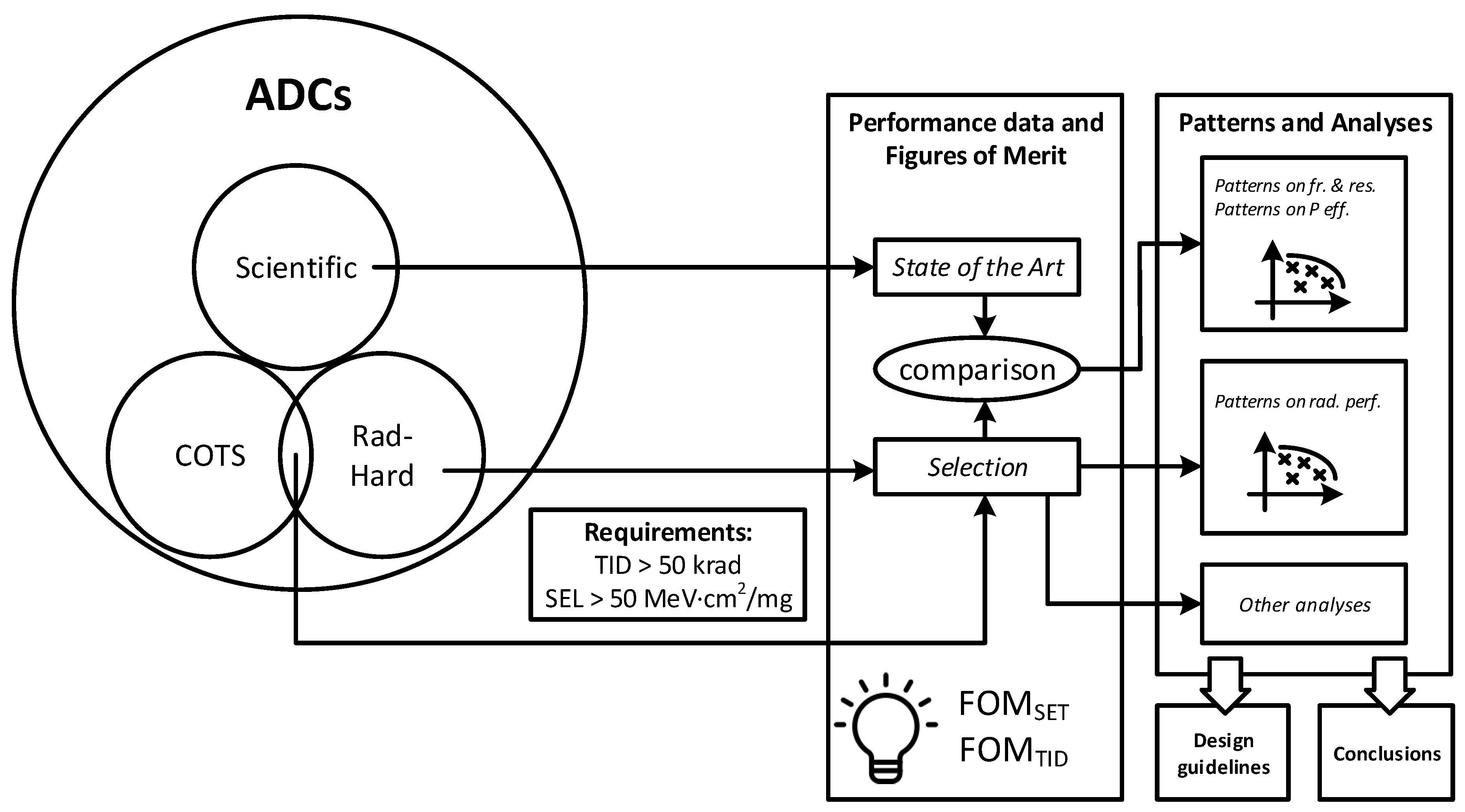
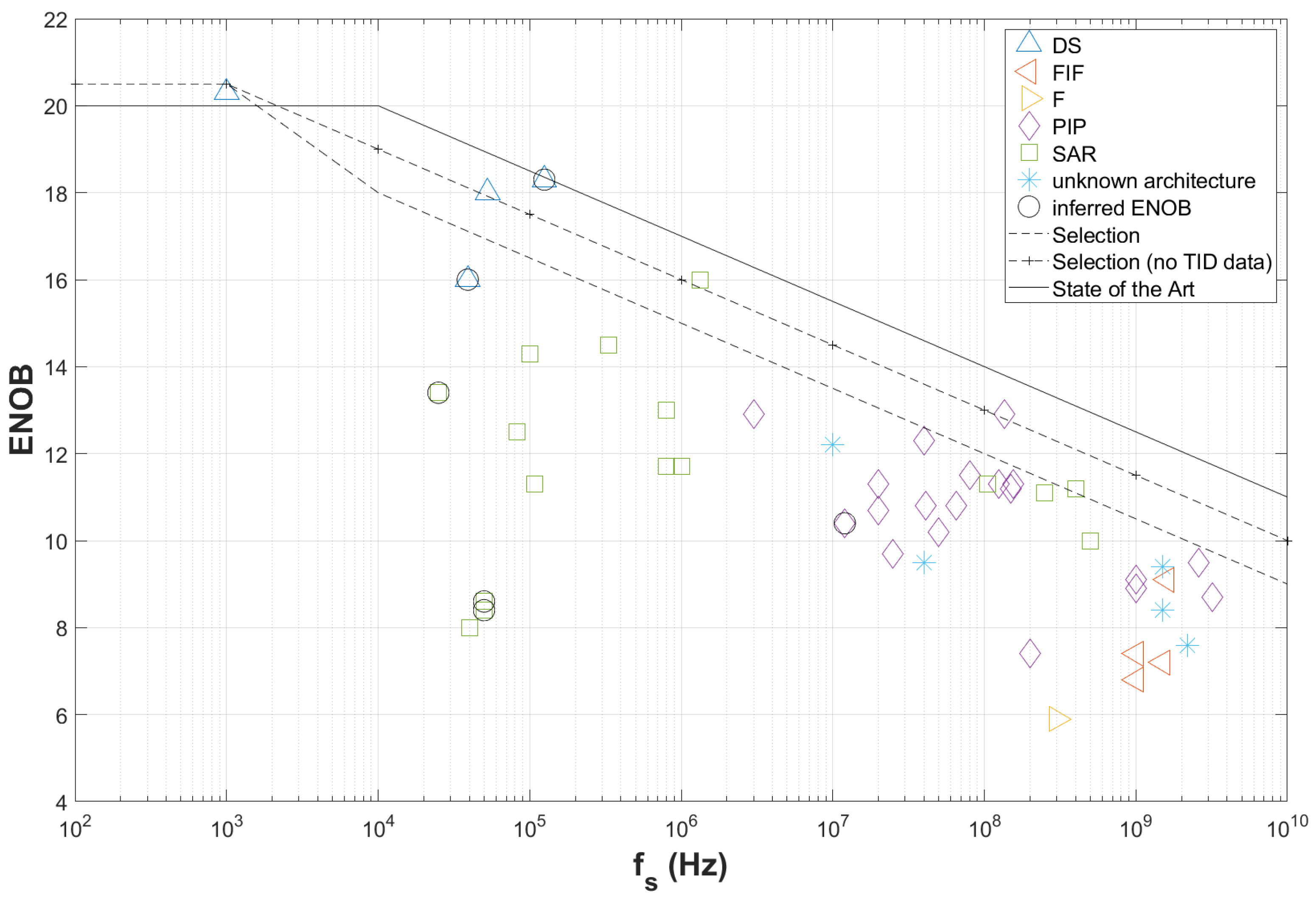
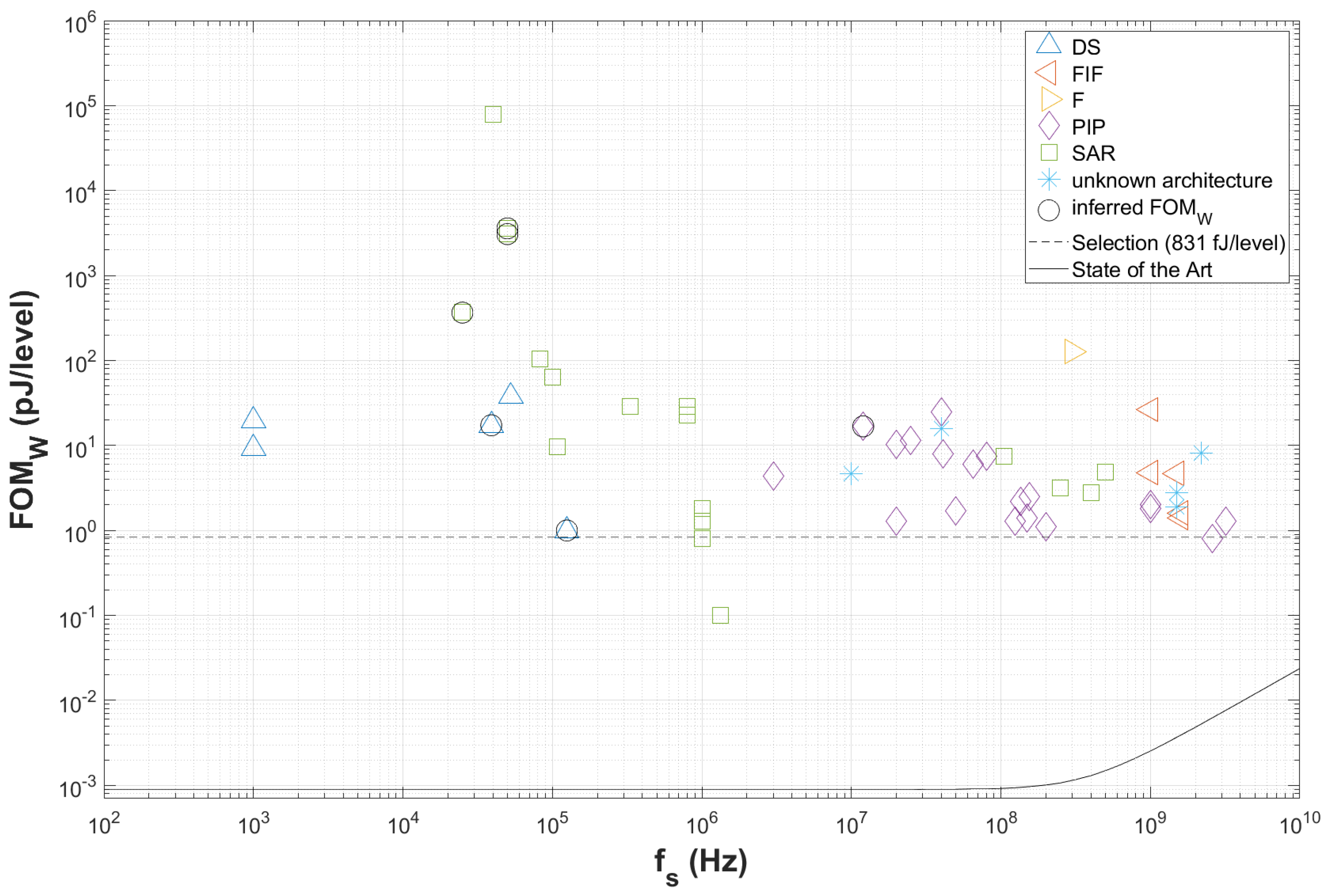
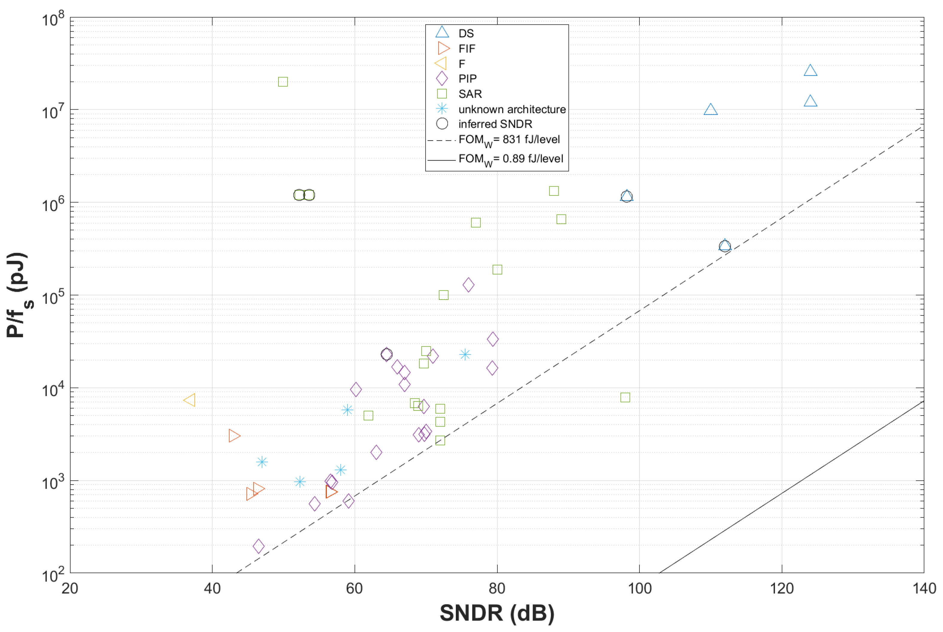
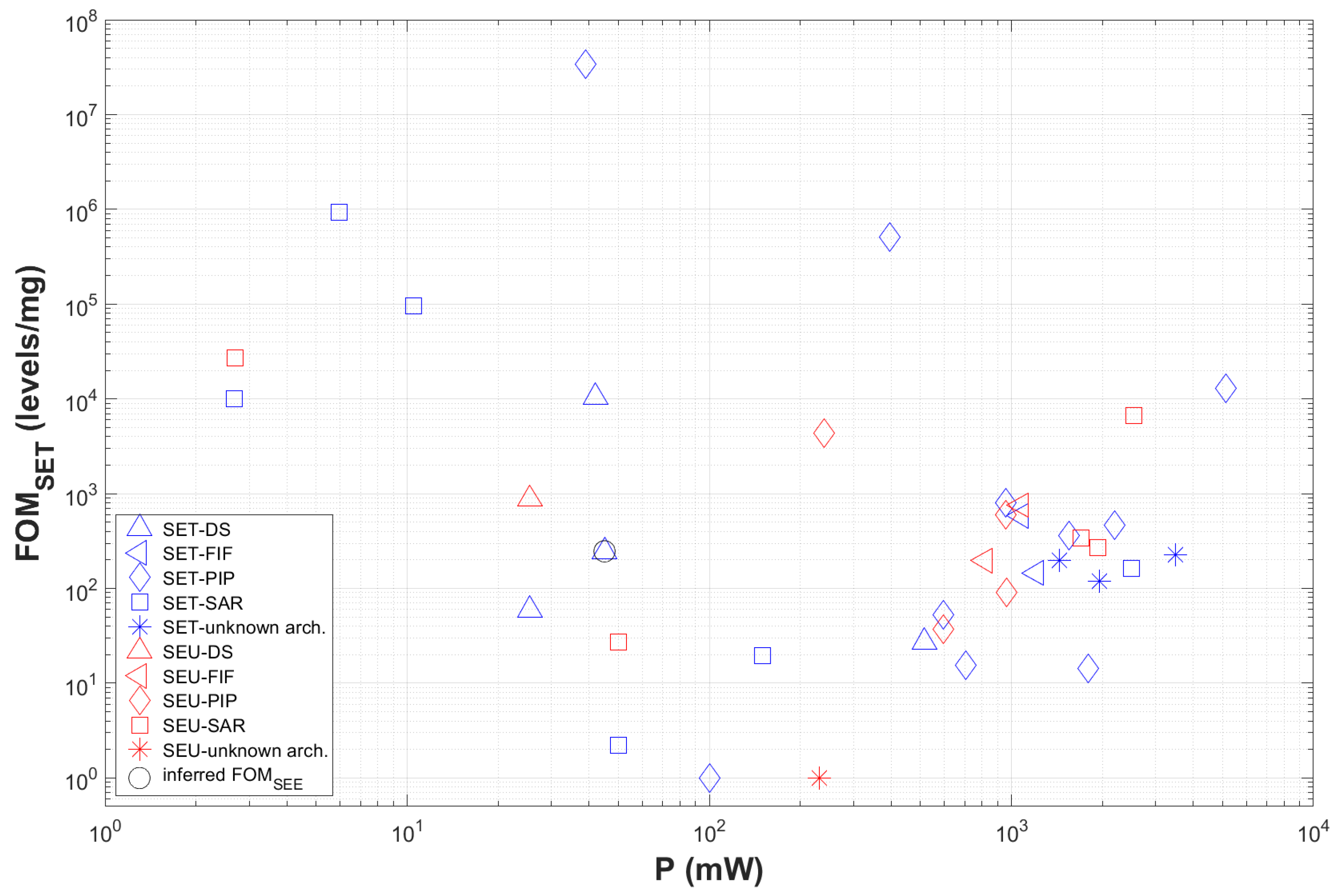
Table 1.
Selection of radenv-ADCs.

Table 2.
Detection methods of soft errors in radenv-ADCs testing.
| # | Test Method | Abbreviation | Reference(s) |
|---|---|---|---|
| 1 | Beat Frequency/Two-Point | BF/2P | [34,37,65,67] |
| 2 | Code Error Rate/Coherent Sampling | CER/CS | [4,51,54,68] |
| 3 | Comparison with DAC input | DAC | [1] |
| 4 | Comparison with ‘golden chip’ | GOLD | [69] |
| 5 | Dynamic Input Signal | DIS | [70] |
| 6 | Four-Point | 4P | [3,34,71,72] |
| 7 | Quasi-Static | QS | [36] |
| 8 | Single-Point | 1P | [3,34,45] |
| 9 | Static | S | [35,37,73,74] |
Table 3.
Operation ranges within the selection segregated by architecture.
| Architecture | Count | ENOB | FOM | |||
|---|---|---|---|---|---|---|
| [MHz] | [pJ/Level] | [Levels/mg] | ||||
| 5 | [16; 20.3] | [0.001; 0.125] | [1; 37.8] | 6 | 2320 | |
| SAR | 19 | [8; 16] | [0.025; 500] | [0.1; 78125] | 34 | 83,313 |
| PIP | 21 | [7.4; 12.9] | [3; 3200] | [0.8; 24.8] | 109 | 2,139,462 |
| FIF | 8 | [6.8; 9.4] | [1000; 2200] | [1.4; 26.5] | 79 | 303 |
Table 4.
Suitability of ADC architectures for applications in radiation environments.
| Application | SAR | PIP | FIF | Flash | ||
|---|---|---|---|---|---|---|
| collider experiments | ✓✓ | ✓ | ||||
| discrete-time control | ✓ | ✓✓ | ✓ | |||
| earth observation | ✓✓ | ✓ | ||||
| house-keeping | ✓ | ✓ | ||||
| satellite communications | base-band | ✓✓ | ✓ | |||
| DDC | ✓✓ | ✓✓ | ✓ | |||
| sensor acquisition | thermistor | ✓✓ | ✓ | |||
| gauge | ✓✓ | ✓ | ||||
| magnetometer | ✓✓ | ✓ | ||||
| star tracker | ✓ | ✓✓ | ||||
| sun sensor | ✓ | ✓✓ | ||||
| telemetry | fast dynamics | ✓ | ||||
| slow dynamics | ✓✓ | ✓ | ||||
| video | ✓ | ✓✓ | ||||
Table 5.
Suitability of ADC soft error test methods for applications in radiation environments.
| Application | BF | CS | DAC | GOLD | DIS | 4P | QS | 1P | S | |
|---|---|---|---|---|---|---|---|---|---|---|
| collider experiments | ✓ | ✓ | ✓ | ✓ | ✓ | ✓ | ||||
| discrete-time control | ✓ | ✓ | ✓ | ✓ | ✓ | ✓ | ||||
| earth observation | ✓ | ✓ | ||||||||
| house-keeping | ✓ | ✓ | ✓ | |||||||
| satellite communications | base-band | ✓ | ✓ | ✓ | ✓ | ✓ | ||||
| DDC | ✓ | ✓ | ✓ | ✓ | ||||||
| sensor acquisition | thermistor | ✓ | ✓ | |||||||
| gauge | ✓ | ✓ | ||||||||
| magnetometer | ✓ | ✓ | ||||||||
| star-tracker | ✓ | ✓ | ✓ | ✓ | ✓ | ✓ | ||||
| sun sensor | ✓ | ✓ | ✓ | ✓ | ✓ | ✓ | ||||
| telemetry | fast dynamics | ✓ | ✓ | ✓ | ✓ | ✓ | ✓ | |||
| slow dynamics | ✓ | ✓ | ||||||||
| video | ✓ | ✓ | ✓ | ✓ | ✓ | ✓ | ||||
Publisher’s Note: MDPI stays neutral with regard to jurisdictional claims in published maps and institutional affiliations. |
© 2020 by the authors. Licensee MDPI, Basel, Switzerland. This article is an open access article distributed under the terms and conditions of the Creative Commons Attribution (CC BY) license (http://creativecommons.org/licenses/by/4.0/).
Share and Cite
MDPI and ACS Style
Pun-García, E.; López-Vallejo, M. A Survey of Analog-to-Digital Converters for Operation under Radiation Environments. Electronics 2020, 9, 1694. https://doi.org/10.3390/electronics9101694
AMA Style
Pun-García E, López-Vallejo M. A Survey of Analog-to-Digital Converters for Operation under Radiation Environments. Electronics. 2020; 9(10):1694. https://doi.org/10.3390/electronics9101694
Chicago/Turabian StylePun-García, Ernesto, and Marisa López-Vallejo. 2020. "A Survey of Analog-to-Digital Converters for Operation under Radiation Environments" Electronics 9, no. 10: 1694. https://doi.org/10.3390/electronics9101694
Note that from the first issue of 2016, this journal uses article numbers instead of page numbers. See further details here.