Growth and Characterization of Cu2MnSnS4 Thin Films Synthesized by Spray Pyrolysis under Air Atmosphere


1
Laboratoire de Photovoltaïque et matériaux semi-conducteurs, Ecole Nationale d’Ingénieurs de Tunis, Université de Tunis El Manar, Tunis 1002, Tunisia
2
Ecole Nationale Supérieure d’Ingénieurs de Tunis, Université de Tunis, 5 Ave Taha Hussein, Tunis 1008, Tunisia
3
FEMTO-ST, UMR 6174, CNRS, Université Bourgogne Franche-Comté, UTBM, Site de Montbéliard, 90010 Belfort, France
*
Author to whom correspondence should be addressed.
Coatings 2020, 10(10), 963; https://doi.org/10.3390/coatings10100963
Submission received: 7 September 2020
/
Revised: 29 September 2020
/
Accepted: 3 October 2020
/
Published: 9 October 2020
(This article belongs to the Section Thin Films)
Abstract
:The direct synthesis of chalcopyrite Cu2MnSnS4 (CMTS) thin films by a spray pyrolysis technique on glass substrates under oxidative conditions (ambient atmosphere and using compressed air as a carrier gas instead of nitrogen) was studied. The effect of the deposition temperature on the structural, chemical composition, and optical and electrical properties of thin films has been assessed. X-ray diffraction study reveals that the tetragonal stannite structure crystallizes with a [112] preferential orientation from 280 up to 360 °C, with its crystallinity correlated with the substrate temperature. However, in addition to its crystallization, traces of secondary phases are observed: a mixture of SnO and CuO at 360 °C prevails on the formation of CuS at 320 °C. Above 360 °C, the oxidant conditions combined with the loss in sulfur lead to the crystallization of only the tenorite CuO. The crystallization of sulfides by spray pyrolysis under air is possible only at relatively low deposition temperature for which the oxidation rate is inefficient compared to the sulfidation rate. Further optical studies of stannite films indicate a high absorption coefficient toward the visible range (>104 cm−1) and an optical band gap of about 1.64–1.85 eV, also depending on the substrate temperature. The CMTS thin films deposited below 360 °C exhibit a moderate electrical resistivity of about Ω·cm at room temperature. The properties of the stannite films synthesized using a spray pyrolysis technique in ambient air are comparable to those of films obtained by spray pyrolysis with nitrogen carrier gas despite the presence of oxides traces, an increase in the deposition temperature improving the microstructure, and its related optical and electrical properties.
1. Introduction
The growth of environmental problems related to the overexploitation of fossil resources is forcing research groups to focus their research on new renewable and clean energies. Solar energy is one of the most important demand of today. A standard photovoltaic device consists in a films stack, from bottom to the top: a Mo back contact layer (~0.5–1 µm), a thick p-type absorber (~1–2.5 µm), thin n-type buffer layer (~0.1 µm), and a transparent conductive oxide contact layer (<~0.5 µm) [1]. The electrical contacts on the top and on the back are necessary to harvest the electrical charges generated by the adsorption of photons. The p–n junction formed by the contact of the n or p doped materials facilitates the separation of electron and holes charges in avoiding their fast recombination after their excitation [2].
One of the major challenges lies in the production of sufficient and inexpensive solar energy while respecting environmental standards. Traditionally, the absorber is based on CuInSe2 (CIS), CuInGa(S,Se)2 (CIGS), or CdTe compounds. The toxicity and the rarety of some elements composing it make crucial the definition of other material. To overcome this problem, recent researches have been focused on absorber composed of earth abundant elements, low-cost to extract and to transform, and non-toxic [3,4]. In this frame, the quaternary diluted magnetic semiconductors sulphides (Cu2−xMxSnS4 with M = Mn, Fe, Co, Ni, Zn, etc.) derivate from the chalcopyrite family. The quaternary sulfides exhibit different polymorphs (tetragonal kesterite I, tetragonal stannite I2m, and cubic F3m…) according to the cation distribution in the tetrahedral site, temperature, or technical synthesis [5,6]. They exhibit interesting photoelectric characteristics relatively close to those of the CIGS reference material [7,8]. Modeling analysis are also reported in view to gain insight into the thermal stability [9]. Among them, copper manganese tin sulfide Cu2MnSnS4 (CMTS) is one of the most promising. Each component of CMTS is abundant in the earth’s crust (Cu: 68 ppm, Mn: 1100 ppm, Sn: 2.2 ppm, S: 420 ppm) [4]. This compound does not exhibit high recombination contrary to the CZTS compound [10]. Further, a direct band gap energy between 1 and 1.5 eV has been reported [11,12] and a large absorption coefficient higher than 104 cm−1 [13]. A power conversion efficiency of 0.76%–0.83% has been achieved recently for CMTS based solar cells [4,14]. In addition, this compound exhibits high radiation stability contrary to the first generation of solar cells for which the application was limited to terrestrial applications [15].
A variety of methods have been used recently to synthesize CMTS, including spray pyrolysis [16,17], sol gel [18,19], direct liquid coating [13], spin coating [20], thermal evaporation [21,22], and electrodeposition [23]. The advantage of the spray pyrolysis technique compared to those mentioned above is its simplicity, its ability to deposit on large areas at lower costs and it is environmentally friendly [24]. The structure and microstructure of the CMTS film depend on the crystallization temperature, and hence strongly influence the efficiency of quaternary chalcogenide thin film solar cells [16,25]. The objective of the present work is to study the direct deposition of CMTS thin films under ambient atmosphere by spray pyrolysis technique using a compressed air as a carrier gas instead of nitrogen. A complete compressed air system meets modern demands in terms of budget, accessibility and respect for the environment and is coherent with cheap photovoltaic industry (low-cost raw materials and production). No supplementary step of sulfurization treatment leading to variable results was used to synthesize crystallized phase [26,27]. Furthermore, researches have dealt with the sulfidation of oxides at 300 °C [28,29], and a previous study on the optical properties of CMTS has already demonstrated the feasibility to deposit this phase by spray pyrolysis under a relatively oxidant atmosphere without providing more detailed information [30]. Because of the potential influence of the synthesis temperature on the structure and the microstructure, the deposition temperature was varied from 280 to 400 °C, and the structural, chemical composition, optical, and electrical characteristics were then assessed.
2. Materials and Methods
2.1. Elaboration
Cu2MnSnS4 (CMTS) thin films have been successfully grown, in our laboratory, using a chemical spray technique on glass substrates in ambient atmosphere using one step-method without post-sulfurization. The experimental setup that was utilized to spray CMTS thin films consists of a substrate heating system and a spray head moving in the x–y plane parallel to the substrate surface in order to achieve a uniform coating on the heated substrates. Before the deposition, the glass substrates with dimension of 2 × 2 cm2 were cleaned with a detergent, washed with 3% nitric acid, rinsed in succession with distilled water and acetone, and finally dried in an oven at 120 °C for 15 min.
For deposition, the starting solutions were prepared in four different glass bottles consisting of SC(NH2)2 (32 mmol), MnCl2·4H2O (2 mmol), SnCl2·2H2O (2 mmol) and CuCl2·2H2O (4 mmol), respectively, by dissolving in distilled water as the solvent agent. The solutions were then mixed in a beaker under magnetic stirring for a few second. HCl (0.5 mL) was also added in order to obtain a homogenous, colorless, and transparent solution. The precursors were taken in stoichiometric composition of CMTS except of thiourea, which, due to its volatility, was taken in excess to prevent any deficiency of sulfur during the spraying. Compressed air was used as a carrier gas. In order to optimize the deposition temperature, the CMTS solution (100 mL) was sprayed onto a heated glass substrate at 280, 320, 360, and 400 °C with a fixed deposition time of 30 min in air. Other deposition parameters of the spraying system including the spray deposition rate, the gas flow rate, the distance nozzle-substrate and the hot plate rotation speed were set at: 3 × 10⁻³ L/min, 10 L/min, 20 cm, and 14 rpm, respectively. After deposition, the final samples were naturally cooled down at room temperature.
The first step of the formation mechanism of CMTS films corresponds to the dissolution of the precursors in the solvent according to these chemical equations as also reported in CCTS thin films by Maldar et al. [31]:
CuCl2 → Cu2+ + 2Cl−
MnCl2 → Mn2+ + 2Cl−
SnCl2 → Sn2+ + 2Cl−
SC(NH2)2 → S2− + H+ + NH2−C=NH
Then, once spraying onto the glass substrates, the formation of CMTS thin films under thermal decomposition can be explained by the following overall equation:
2CuCl2 + MnCl2 + SnCl2 + 4CH4N2S + 10H2O → Cu2MnSnS4 + 8NH4Cl↑ + 4CO2↑ + 2H2O↑
2.2. Characterization
The structural features of the coatings were investigated by using X-ray diffraction (XRD, Philips X’Pert diffractometer, El manar, Tunisia) with Cu-Kα1 radiation (λ = 1.5406 Å) operated in the scanning angle 2θ from 20° to 70°. The operation voltage and current for the XRD patterns were 40 kV and 30 mA, respectively. The chemical composition of the film deposited on glass substrates was estimated by energy dispersive spectroscopy (EDS, Quantax Bruker with XFlash 6|30, Bruker nano, Berlin, Germany). The total transmittance and reflectance of the coatings were measured with a double beam UV-VIS-NIR spectrophotometer (Shimadzu 3100 S, El manar, Tunisia) equipped by integrating sphere (LISR3200, El manar, Tunisia) in the wavelength range of 300–1800 nm in order to determine the optical parameters such as the absorption coefficient and the band gap energy. Resistivity measurements were made on the CMTS film deposited on glass substrates, at room temperature by the four-probe technique. The device is composed by a certified Jandel cell (Multi height probe, Jandel Engineering Limited, Lindslade, UK), the factor form is well known, and it is connected with an HP 3458A multimeter (Agilent, Massy, France) to measure electrical parameters.
3. Results and Discussion
3.1. Structural Characterization
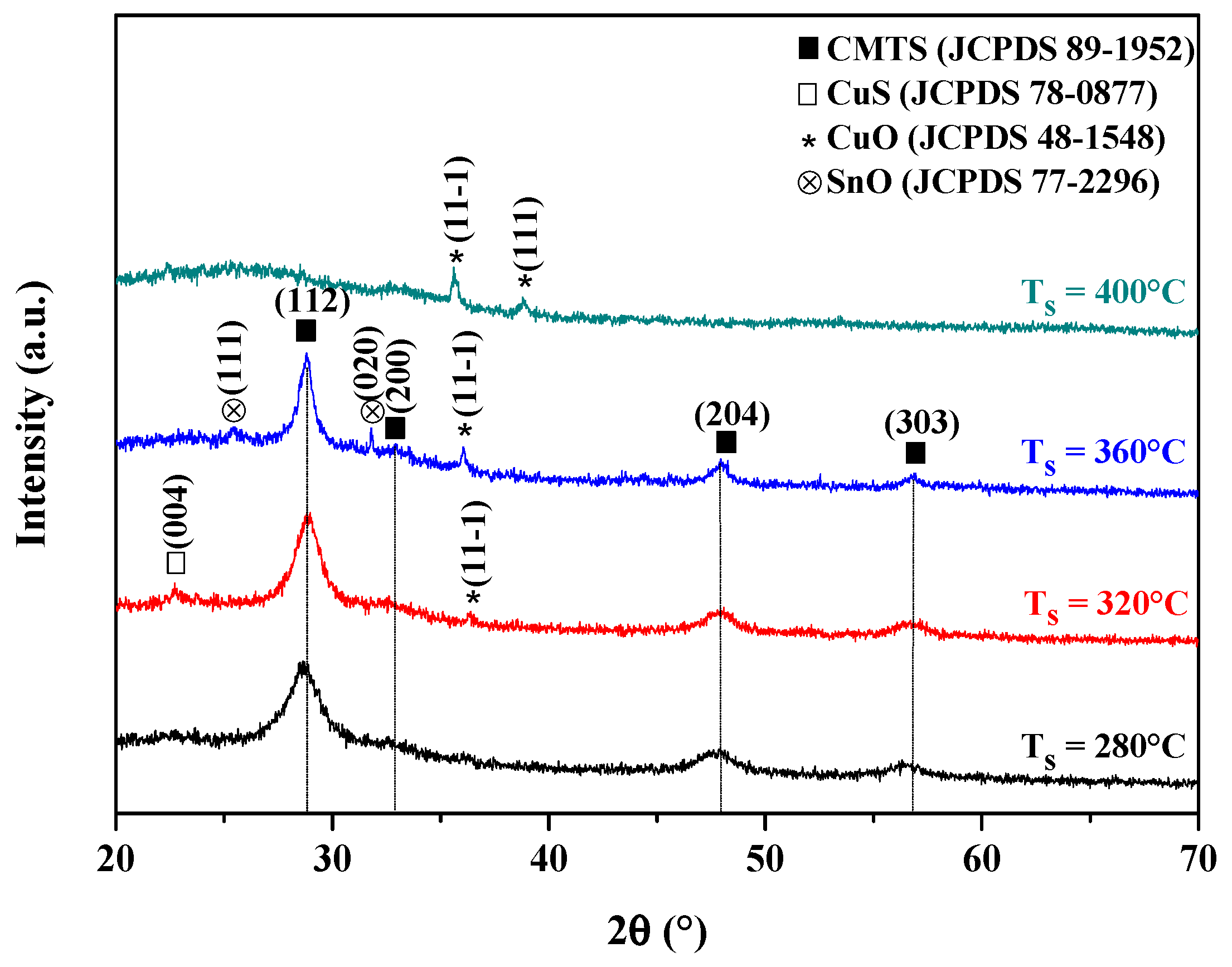
Figure 1 shows the XRD patterns of the as-sprayed films deposited at different substrate temperatures. For the films deposited at substrate temperatures of 280 up to 360 °C, four major peaks can be noted corresponding to the reflections (112), (200), (204), and (303) of the CMTS phase (JCPDS card no. 89-1952), respectively. The CMTS crystallizes in the tetragonal stannite structure with the space group I2m. As the substrate temperature increases from 280 to 360 °C, the intensity and the sharpness of the CMTS peaks increase, showing an improvement of the crystalline quality.
Since the CMTS is a quaternary compound, the crystallization of secondary phases is possible. Taking into account that the deposition occurs in ambient air on heated substrate using a compressed air as a carrier gas and in agreement with the values of the standard Gibb’s energies of formation of simple oxides or sulfides in the corresponding range of temperature, the crystallization of oxides could prevail on that of sulfide compounds. At 280 °C, no trace of impurity phases is X-ray detected, but it is still probable that a small proportion of amorphous oxide could be present. With a further increase at 320 °C, traces of tenorite copper oxide and copper sulfide (CuS) is observed in addition to CMTS phases. At 360 °C, only oxide secondary phases (SnO and CuO) are detected. For further increase of the substrate temperature (Ts) up to 400 °C, the instable SnO is no more observable, and the crystallization of the tenorite CuO prevails over the sulfide crystallization [32,33].
The structural parameters like reticular distance (dhkl), lattice parameters (a, b and c), full-width-at-half-maximum (β), the average crystallite size (Dav), microstrain (ε), and dislocation density (δ) were determined. By using the main peak of (112), the inter reticular distance dhkl values were calculated according to the Bragg equation [34]:
Nλ = 2dhklsinθ
As mentioned above, the CMTS thin films represent a tetragonal stannite structure which leads to (a = b ≠ c). Therefore, the lattice parameters were determined by using the reticular distance formula:
The average crystallite size (Dav) was calculated using the Scherrer formula [35]:
where k is the shape factor (k = 0.9) assuming spherical shape for which the crystallite size is independent of the crystallographic direction, λ is the X-ray wavelength (1.5406 Å), β is the full-width-at-half-maximum (FWHM), and θ is the Bragg diffraction angle.
The microstrain (ε) can be expressed as follows [36]:
The dislocation density (δ) can be evaluated by Williamson and Smallman’s formula [37]:
The detailed data, involving the main structural parameters of the stannite CMTS phase, are listed in Table 1. The average crystallite size (Dav) grows significantly from 5.45 to 12.05 nm with increasing substrate temperature from 280 to 360 °C. This effect associated with the increase of the relative intensity of the diffraction peaks and with the progressive decrease of the microstrain and dislocation density demonstrate an improvement of the crystalline quality with the increase of the substrate temperature in agreement with other reported study [19]. The interplanar spacing is almost constant of all CMTS thin films. The lattice constants a and c (Table 1) are in good agreement with the reported values [19]. The evaluation of ratios of lattice parameters (η = c/2a) of the CMTS thin films is almost constant and they are found to be less than united, which confirms the stannite structure. This result is consistent with those cited in literature [38]. The constancy of the lattice parameters and the crystallization of minor oxide phases would suggest that the growing CMTS phase does not contain oxygen.
3.2. Chemical Composition Characterization
Table 2 lists the composition ratios of the CMTS thin films deposited at different substrate temperatures. All the CMTS thin films show a near stoichiometry metal atomic ratio but with a deficiency of S. However, as observed from this table, the rise of substrate temperature leads to a slight increase of the Cu relatively to the Mn and Sn atoms, and to a slight decrease of Sn content relatively to the Mn and Cu contents. In addition, the S/metals ratio decreases drastically when increasing the substrate temperature above 320 °C, probably due to the higher volatility of sulfur at elevated temperatures, despite the excess of thiourea in the precursor solution [31], and also because of the crystallization of oxides with temperature. The strong loss in sulfur (>50%) combined with the slight change in the stoichiometry of the metal elements at 400 °C explain the non-crystallization of the CMTS phase and the presence of the oxide phase only. In spite of the rather poor accuracy of the EDS technique to measure the oxygen content, it is worth of noting, based on XRD results, that the proportion of oxide phases in CMTS films is increasing with the rise of the substrate temperature. Then an increase of the oxygen content with the deposition temperature is expecting, which contributes to the prevention of sulfurization of the growing films. In agreement with XRD results, the crystallization of sulfides by spray pyrolysis under air is possible only at a relatively low deposition temperature for which the sulfidation conditions remains more efficient than the oxidation.
3.3. Optical Characterization
The optical properties including the measurement of the absorption coefficient and the band gap energy of CMTS thin films were investigated by using UV-Vis spectroscopy. Indeed, the absorption coefficients and the band gap energies were determined from the experimental transmittance (T) and reflectance (R) spectra using these equations, neglecting scattering phenomena [39,40]:
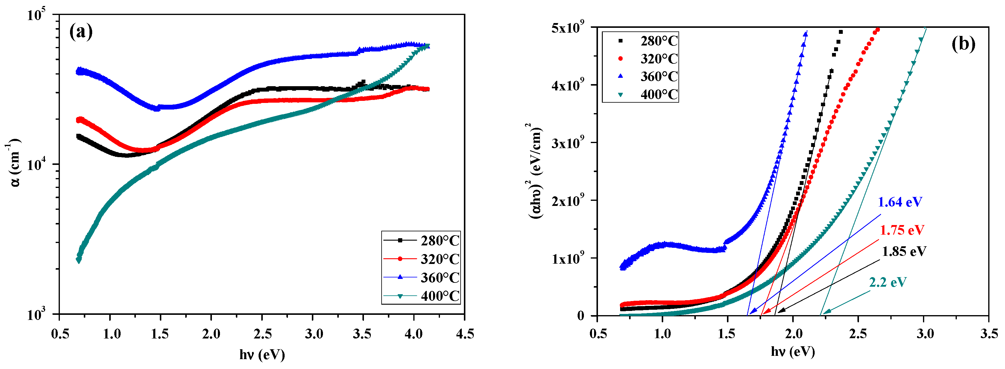
where α and Eg characterize the absorption coefficient and the band gap energy, respectively, d is the coating thickness, A is a constant, h is the Planck’s constant, ν is the incident light frequency, and n is equal to 1/2 for the direct band gap material. The Figure 2a,b shows the variations of the absorption coefficient (α) and the (αhν)2 as a function of photon energy (hν), respectively. From Figure 2a, all the films exhibit absorption coefficients higher than 104 cm−1 towards the visible light region. However, the absorption coefficient of the film deposited at 400 °C corresponding to the CuO phase strongly decreases to 2 × 103 cm−1 in the infrared (λ > 1600 nm), due to the non–crystallization of the tetragonal CMTS phase. These high absorption coefficients are consistent with other reports [41,42] and are considered as suitable absorber layer in thin film solar cell.
Referring to Figure 2b, the band gap energies of the films were deduced by extrapolating the linear portion of the plots to the photon energies axis. The extracted band gap energies of all the films deposited at 280, 320, 360, and 400 °C are found to be 1.85, 1.75, 1.64, and 2.2 eV, respectively. For the films crystallizing with the tetragonal phase with only minor phases, one can observe a decrease of the band gap when increasing the substrate temperature. However, these values are slightly higher than that those reported in literature (Eg ~1.23–1.45 eV) [25,43]. The crystallization of secondary phases having higher band gap values than that of the CMTS phase explain the higher observed band gap energy range of the films deposited from 280 to 360 °C. Indeed, the possibility to tune the optical band gap as a function of the proportion of phases in composite film has already been reported [44]. Nie et al. have also observed an increase of the band gap energy in CMTS films due to the crystallization of sulfide impurity which exhibits a band gap energy of about 2 eV as deposited [16]. Furthermore, the decrease of the optical band gap with the deposition temperature is coherent with the crystallization of secondary phases having an increasingly smaller band gap energy with the elevation of the deposition temperature (e.g., CuS ~3.5–3.8 eV [45], SnO ~2.5–2.9 eV [46], CuO ~1.2–2.2eV [47,48]). In addition, other factors could also contribute to the observed bandgap decrease: the Cu enrichment of the tetragonal phase associated with the sulfur loss, as observed by EDS, could change the degree of hybridization [25,49], and the improvement of crystalline quality of the main CMTS phase would lead to a lower number of structural defects and grain boundaries in agreement with XRD results.
It is worth of noting that an increase of the deposition temperature at 360 °C leads to a superior absorption coefficient in the visible range due, on the one hand, to the lower band gap energy resulting in a widening of the spectral window, and on the other hand, to the enhancement of the crystallinity.
3.4. Electrical Characterization
The electrical resistivity at room temperature of the CMTS thin films has been measured using a four-probe method. As presented in Table 3, the resistivity of CMTS thin films slowly decreases from 3.38 to 1.14 Ω·cm as the substrate temperature increases from 280 to 360 °C, and then increases significantly to 9.53 × 10⁴ Ω·cm with further prolonging substrate temperature to 400 °C which is ascribed to the presence of the CuO phase. This value is rather coherent with other electrical resistivities of copper oxide previously reported [50,51]. The electrical resistivity values of the optimum CMTS thin films are near to the values of CZTS thin films doped Al obtained by Gadallah et al. [52]. The slow decrease of the electrical resistivity is favored by the crystallinity improvement such as the crystallite growth [53], and also by the higher metal enrichment due to the sulfur loss with the temperature increases.
4. Conclusions
The tetragonal structured CMTS thin films have been elaborated by a spray pyrolysis technique on a heated glass substrate in air atmosphere and using a compressed air as a carrier gas. Despite rather oxidative conditions, it was shown that the tetragonal CMTS crystallizes as a dominant phase with a preferential orientation [112] for a moderate deposition temperature (<400 °C). The improvement in the crystalline quality of the CMTS thin films is correlated with the substrate temperature. With the increase of the deposition temperature, a small and progressive oxidation of the growing film occurs, leading to the formation of oxides traces at elevated temperatures prevailing over the formation of sulfides at lower temperatures. The crystalline quality improvement with the deposition temperature increase at 360 °C results in a high absorption coefficient (<104 cm−1) in the visible range, and a rather low electrical resistivity of about Ω·cm. The bandgap energy is close to 1.64 eV. It is demonstrated that these properties are suitable as a solar absorber in low-cost solar cells, even if impurity traces can crystallize. Further analyses, such as TEM, XPS, EPMA, EELS, and photoelectrical response could be useful to gain a deeper insight into the properties of the material studied, but they are beyond the scope of the present analysis. From an engineering point of view, the deposition of sulfide under air atmosphere can be an asset to facilitate a cheap solar cell process. The stacks could be strengthened by the oxides crystallization to promote the mechanical adhesion when implementing a chemical gradient, or in tuning the spectral sensitivity in a multiple junction solar cell.
Author Contributions
Data curation, S.D. and E.A.; formal analysis, E.A.; project administration, P.B.; resources, P.B.; software, E.A.; supervision, N.B. and P.B.; writing—original draft, S.D. and E.A.; writing—review & editing, N.B., F.C. and P.B. All authors have read and agreed to the published version of the manuscript.
Funding
The authors are indebted to the Pays of Montbéliard Agglomération (PMA) for its financial support.
Acknowledgments
The authors are grateful to the Tunisian Ministry of Higher Education and Scientific Research for financial support of this work. This work was done within the FEMTO-ST SURFACE platform.
Conflicts of Interest
The authors declare no conflict of interest.
References
- Parisi, A.; Pernice, R.; Rocca, V.; Curcio, L.; Stivala, S.; Cino, A.C.; Cipriani, G.; Di Dio, V.; Galluzzo, G.R.; Miceli, R.; et al. Graded Carrier Concentration Absorber Profile for High Efficiency CIGS Solar Cells. Int. J. Photoenergy 2015, 2015, 1–9. [Google Scholar] [CrossRef]
- Fillon, R. Etude des Propriétés Electroniques de Couches Minces de CZTSSe. Ph.D. Thesis, Université de Grenoble, Grenoble, French, October 2016. [Google Scholar]
- Zhang, X.; Bao, N.; Ramasamy, K.; Wang, Y.-H.A.; Wang, Y.; Lin, B.; Gupta, A. Crystal phase-controlled synthesis of Cu2FeSnS4 nanocrystals with a band gap of around 1.5 eV. Chem. Commun. 2012, 48, 4956. [Google Scholar] [CrossRef] [PubMed]
- Le Donne, A.; Trifiletti, V.; Binetti, S. New Earth-Abundant Thin Film Solar Cells Based on Chalcogenides. Front. Chem. 2019, 7, 297. [Google Scholar] [CrossRef] [PubMed] [Green Version]
- Evstigneeva, T.L.; Kabalov, Y.K. Crystal structure of the cubic modification of Cu2FeSnS4. Crystallogr. Rep. 2001, 46, 368–372. [Google Scholar] [CrossRef]
- Fries, T.; Shapira, Y.; Palacio, F.; Moron, M.C.; McIntyre, G.J.; Kershaw, R.; Wold, A.; McNiff, E.J. Magnetic ordering of the antiferromagnet Cu2MnSnS4 from magnetization and neutron-scattering measurements. Phys. Rev. B 1997, 56, 5424–5431. [Google Scholar] [CrossRef] [Green Version]
- Ghosh, A.; Biswas, A.; Thangavel, R.; Udayabhanu, G. Photo-electrochemical property and electronic band structure of kesteritecopper chalcogenides Cu2-II-Sn-S4 (II = Fe, Co, Ni) thin films. RSC Adv. 2016, 6, 96025–96034. [Google Scholar] [CrossRef]
- Chatterjee, S.; Pal, A.J. A solution approach to p-type Cu2FeSnS4 thin-films and pn-junction solar cells: Role of electron selective materials on their performance. Sol. Energy Mater. Sol. Cells 2017, 160, 233–240. [Google Scholar] [CrossRef]
- Zandi, S.; Saxena, P.; Razaghi, M.; Gorji, N.E. Simulation of CZTSSe Thin-Film Solar Cells in COMSOL: Three-Dimensional Optical, Electrical, and Thermal Models. IEEE J. Photovolt. 2020, 10, 1503–1507. [Google Scholar] [CrossRef]
- Siebentritt, S. Why are kesterite solar cells not 20% efficient? Thin Solid Film. 2013, 535, 1–4. [Google Scholar] [CrossRef] [Green Version]
- Ozel, F. Earth-abundant quaternary semiconductor Cu2MSnS4 (M = Fe, Co, Ni and Mn) nanofibers: Fabrication, characterization and band gap arrangement. J. Alloy. Compd. 2016, 657, 157–162. [Google Scholar] [CrossRef]
- Cui, Y.; Deng, R.; Wang, G.; Pan, D. A general strategy for synthesis of quaternary semiconductor Cu2MSnS4 (M = Co2+, Fe2+, Ni2+, Mn2+) nanocrystals. J. Mater. Chem. 2012, 22, 23136–23140. [Google Scholar] [CrossRef]
- Chen, L.; Deng, H.; Tao, J.; Cao, H.; Sun, L.; Yang, P.; Chu, J. Strategic improvement of Cu2MnSnS4 films by two distinct post-annealing processes for constructing thin film solar cells. Acta Mater. 2016, 109, 1–7. [Google Scholar] [CrossRef]
- Yu, J.; Deng, H.; Chen, L.; Tao, J.; Zhang, Q.; Guo, B.; Sun, L.; Yang, P.; Zheng, X.; Chu, J. Improvement performance of two-step electrodepositing Cu2MnSnS4 thin film solar cells by tuning Cu-Sn alloy layer deposition time. Mater. Chem. Phys. 2018, 211, 382–388. [Google Scholar] [CrossRef]
- Woodyard, J.R.; Landis, G.A. Radiation resistance of thin-film solar cells for space photovoltaic power. Sol. Cells 1991, 31, 297–329. [Google Scholar] [CrossRef] [Green Version]
- Nie, L.; Yang, J.; Yang, D.; Zhang, W. Effect of substrate temperature on growth and properties of Cu2MnSnS4 thin films prepared by chemical spray pyrolysis. J. Mater. Sci. Mater. Electron. 2019, 30, 3760–3766. [Google Scholar] [CrossRef]
- Prabhakar, R.R.; Zhenghua, S.; Xin, Z.; Baikie, T.; Woei, L.S.; Shukla, S.; Batabyal, S.K.; Gunawan, O.; Wong, L.H. Photovoltaic effect in earth abundant solution processed Cu2MnSnS4 and Cu2MnSn(S,Se)4 thin films. Sol. Energy Mater. Sol. Cells 2016, 157, 867–873. [Google Scholar] [CrossRef]
- Chen, L.L.; Deng, H.M.; Zhang, K.Z.; Huang, L.; Liu, J.; Sun, L.; Yang, P.X.; Chu, J.H. Structural and Optical Properties of Cu2MnSnS4 Thin Film Fabricated by Sol-Gel Technique. Mater. Sci. Forum 2015, 814, 39–43. [Google Scholar] [CrossRef]
- Chen, L.; Deng, H.; Tao, J.; Zhou, W.; Sun, L.; Yue, F.; Yang, P.; Chu, J. Influence of annealing temperature on structural and optical properties of Cu2MnSnS4 thin films fabricated by sol–gel technique. J. Alloy. Compd. 2015, 640, 23–28. [Google Scholar] [CrossRef]
- Chen, L.; Deng, H.; Tao, J.; Cao, H.; Huang, L.; Sun, L.; Yang, P.; Chu, J. Synthesis and characterization of earth-abundant Cu2MnSnS4 thin films using a non-toxic solution-based technique. RSC Adv. 2015, 5, 84295–84302. [Google Scholar] [CrossRef]
- Marchionna, S.; Le Donne, A.; Merlini, M.; Binetti, S.; Acciarri, M.; Cernuschi, F. Growth of Cu2MnSnS4 PV absorbers by sulfurization of evaporated precursors. J. Alloy. Compd. 2017, 693, 95–102. [Google Scholar] [CrossRef]
- Le Donne, A.; Marchionna, S.; Acciarri, M.; Cernuschi, F.; Binetti, S. Relevant efficiency enhancement of emerging Cu2MnSnS4 thin film solar cells by low temperature annealing. Sol. Energy 2017, 149, 125–131. [Google Scholar] [CrossRef]
- Yu, J.; Deng, H.; Tao, J.; Chen, L.; Cao, H.; Sun, L.; Yang, P.; Chu, J. Synthesis of Cu2MnSnS4 thin film deposited on seeded fluorine doped tin oxide substrate via a green and low-cost electrodeposition method. Mater. Lett. 2017, 191, 186–188. [Google Scholar] [CrossRef]
- Perednis, D.; Gauckler, L.J. Thin Film Deposition Using Spray Pyrolysis. J. Electroceramics 2005, 14, 103–111. [Google Scholar] [CrossRef]
- Yu, J.; Deng, H.; Zhang, Q.; Tao, J.; Sun, L.; Yang, P.; Chu, J. The role of sulfurization temperature on the morphological, structural and optical properties of electroplated Cu2MnSnS4 absorbers for photovoltaics. Mater. Lett. 2018, 233, 111–114. [Google Scholar] [CrossRef]
- Prabhakar, R.R.; Loc, N.H.; Kumar, M.H.; Boix, P.P.; Juan, S.; John, R.A.; Batabyal, S.K.; Wong, L.H. Facile Water-based Spray Pyrolysis of Earth-Abundant Cu2FeSnS4 Thin Films as an Efficient Counter Electrode in Dye-Sensitized Solar Cells. ACS Appl. Mater. Interfaces 2014, 6, 17661–17667. [Google Scholar] [CrossRef]
- Aboulfadl, H.; Keller, J.; Larsen, J.; Thuvander, M.; Riekehr, L.; Edoff, M.; Platzer-Björkman, C. Microstructural Characterization of Sulfurization Effects in Cu(In,Ga)Se2 Thin Film Solar Cells. Microsc. Microanal. 2019, 25, 532–538. [Google Scholar] [CrossRef]
- Neveux, L.; Chiche, D.; Pérez-Pellitero, J.; Favergeon, L.; Gay, A.-S.; Pijolat, M. New insight into the ZnO sulfidation reaction: Mechanism and kinetics modeling of the ZnS outward growth. Phys. Chem. Chem. Phys. 2013, 15, 1532–1545. [Google Scholar] [CrossRef] [Green Version]
- Van Der Vlies, A.J.; Kishan, G.; Niemantsverdriet, J.; Prins, A.R.; Weber, T. Basic Reaction Steps in the Sulfidation of Crystalline Tungsten Oxides. J. Phys. Chem. B 2002, 106, 3449–3457. [Google Scholar] [CrossRef]
- Hassanien, A.S.; El Radaf, I.M. Optical characterizations of quaternary Cu2MnSnS4 thin films: Novel synthesis process of film samples by spray pyrolysis technique. Phys. B: Condens. Matter 2020, 585, 412110. [Google Scholar] [CrossRef]
- Maldar, P.; Gaikwad, M.; Mane, A.; Nikam, S.; Desai, S.; Giri, S.; Sarkar, A.; Moholkar, A. Fabrication of Cu2CoSnS4 thin films by a facile spray pyrolysis for photovoltaic application. Sol. Energy 2017, 158, 89–99. [Google Scholar] [CrossRef]
- Miller, S.A.; Gorai, P.; Aydemir, U.; Mason, T.O.; Stevanović, V.; Toberer, E.S.; Snyder, G.J. SnO as a potential oxide thermoelectric candidate. J. Mater. Chem. C 2017, 5, 8854–8861. [Google Scholar] [CrossRef]
- Bikowski, A.; Holder, A.; Peng, H.; Siol, S.; Norman, A.G.; Lany, S.; Zakutayev, A. Synthesis and Characterization of (Sn,Zn)O Alloys. Chem. Mater. 2016, 28, 7765–7772. [Google Scholar] [CrossRef]
- Kacher, J.; Landon, C.; Adams, B.L.; Fullwood, D. Bragg’s Law diffraction simulations for electron backscatter diffraction analysis. Ultramicroscopy 2009, 109, 1148–1156. [Google Scholar] [CrossRef] [PubMed]
- Barret, C.; Massalki, T.B. Structure of Metals; Pergamon Press: Oxford, UK, 1980. [Google Scholar] [CrossRef]
- Jebali, A.; Khemiri, N.; Kanzari, M. The effect of annealing in N2 atmosphere on the physical properties of SnSb4S7 thin films. J. Alloy. Compd. 2016, 673, 38–46. [Google Scholar] [CrossRef]
- Williamson, G.K.; Smallman, R.E., III. Dislocation densities in some annealed and cold-worked metals from measurements on the X-ray debye-scherrer spectrum. Philos. Mag. 1956, 1, 34–46. [Google Scholar] [CrossRef]
- Khadka, D.B.; Kim, J. Structural, optical and electrical properties of Cu2FeSnX4 (X = S, Se) thin films prepared by chemical spray pyrolysis. J. Alloy. Compd. 2015, 638, 103–108. [Google Scholar] [CrossRef]
- Milovzorov, D.; Ali, A.; Inokuma, T.; Kurata, Y.; Suzuki, T.; Hasegawa, S. Optical properties of silicon nanocrystallites in polycrystalline silicon films prepared at low temperature by plasma-enhanced chemical vapor deposition. Thin Solid Film. 2001, 382, 47–55. [Google Scholar] [CrossRef]
- Davis, E.A.; Mott, N.F. Conduction in non-crystalline systems V. Conductivity, optical absorption and photoconductivity in amorphous semiconductors. Philos. Mag. 1970, 22, 0903–0922. [Google Scholar] [CrossRef]
- Dridi, S.; Bitri, N.; Abaab, M. Synthesis of quaternary Cu2NiSnS4 thin films as a solar energy material prepared through «spray» technique. Mater. Lett. 2017, 204, 61–64. [Google Scholar] [CrossRef]
- Adelifard, M. Preparation and characterization of Cu2FeSnS4 quaternary semiconductor thin films via the spray pyrolysis technique for photovoltaic applications. J. Anal. Appl. Pyrolysis 2016, 122, 209–215. [Google Scholar] [CrossRef]
- Chen, L.; Deng, H.; Cui, J.; Tao, J.; Zhou, W.; Cao, H.; Sun, L.; Yang, P.; Chu, J. Composition dependence of the structure and optical properties of Cu2MnxZn1−xSnS4 thin films. J. Alloy. Compd. 2015, 627, 388–392. [Google Scholar] [CrossRef]
- Xie, Z.; Liu, X.; Zhan, P.; Wang, W.; Zhang, Z. Tuning the optical bandgap of TiO2-TiN composite films as photocatalyst in the visible light. AIP Adv. 2013, 3, 062129. [Google Scholar] [CrossRef]
- Nemade, K.; Waghuley, S. Band gap engineering of CuS nanoparticles for artificial photosynthesis. Mater. Sci. Semicond. Process. 2015, 39, 781–785. [Google Scholar] [CrossRef]
- Peng, H.; Bikowski, A.; Zakutayev, A.; Lany, S. Pathway to oxide photovoltaics via band-structure engineering of SnO. APL Mater. 2016, 4, 106103. [Google Scholar] [CrossRef]
- Murali, D.S.; Kumar, S.; Choudhary, R.J.; Wadikar, A.D.; Jain, M.K.; Subrahmanyam, A. Synthesis of Cu2O from CuO thin films: Optical and electrical properties. AIP Adv. 2015, 5, 047143. [Google Scholar] [CrossRef]
- Al-Ghamdi, A.A.; Khedr, M.; Ansari, M.S.; Hasan, P.; Abdel-Wahab, M.S.; Farghali, A. RF sputtered CuO thin films: Structural, optical and photo-catalytic behavior. Phys. E Low-Dimens. Syst. Nanostruct. 2016, 81, 83–90. [Google Scholar] [CrossRef]
- Chen, S.; Walsh, A.; Yang, J.-H.; Gong, X.G.; Sun, L.; Yang, P.-X.; Chu, J.-H.; Wei, S.-H. Compositional dependence of structural and electronic properties of Cu2ZnSn(S,Se)4 alloys for thin film solar cells. Phys. Rev. B 2011, 83, 125201. [Google Scholar] [CrossRef] [Green Version]
- Valladares, L.D.L.S.; Salinas, D.H.; Dominguez, A.B.; Najarro, D.A.; Khondaker, S.I.; Mitrelias, T.; Barnes, C.H.W.; Aguiar, J.A.; Majima, Y. Crystallization and electrical resistivity of Cu2O and CuO obtained by thermal oxidation of Cu thin films on SiO2/Si substrates. Thin Solid Film. 2012, 520, 6368–6374. [Google Scholar] [CrossRef]
- Figueiredo, V.; Elangovan, E.; Goncalves, G.; Barquinha, P.; Pereira, L.; Franco, N.; Alves, E.; Martins, R.; Fortunato, E. Effect of post-annealing on the properties of copper oxide thin films obtained from the oxidation of evaporated metallic copper. Appl. Surf. Sci. 2008, 254, 3949–3954. [Google Scholar] [CrossRef]
- Gadallah, A.-S.; Salim, M.; Atwee, T.; Ghander, A. Effect of Al doping on structural, morphological, optical, and electrical properties of Cu2ZnSnS4 thin films prepared by sol-gel spin coating. Optik 2018, 159, 275–282. [Google Scholar] [CrossRef]
- Horwat, D.; Dehmas, M.; Aubry, E.; Zollinger, J.; Migot, S.; Pierson, J. Properties of nanocrystalline and nanocomposite WxZr1−x thin films deposited by co-sputtering. Intermet. 2009, 17, 421–426. [Google Scholar] [CrossRef]
Figure 1.
X-ray diffractograms of CMTS thin films grown at different substrate temperatures.

Figure 2.
(a) Variation of absorption coefficient (α), and (b) variation of (αhν)2 versus photon energy (hν) of CMTS thin films grown at different substrate temperatures.
Figure 2.
(a) Variation of absorption coefficient (α), and (b) variation of (αhν)2 versus photon energy (hν) of CMTS thin films grown at different substrate temperatures.


Table 1.
Lattice constants of the CMTS thin films deposited at different substrate temperatures.
| Ts (°C) | FWHM of (112) Peak (Degree) | Interplanar Spacing of (112) (Å) | Lattice Constant a (Å) | Lattice Constant c (Å) | Crystallite Size D (nm) | ε (10−1) | δ (10−2 nm−2) | ||
|---|---|---|---|---|---|---|---|---|---|
| 280 | 1.508 | 3.13 | 5.49 | 10.72 | 0.97 | 5.45 | 1.48 | 3.36 | |
| 320 | 1.211 | 3.09 | 5.48 | 10.74 | 0.97 | 6.79 | 1.17 | 2.16 | |
| 360 | 0.684 | 3.09 | 5.44 | 10.55 | 0.96 | 12.05 | 0.66 | 0.68 | |
Table 2.
Composition ratios of the CMTS thin films deposited at different substrate temperatures.
| Ts (°C) | Composition Ratios | ||
|---|---|---|---|
| Cu/(Sn + Mn) | Mn/Sn | S/Metals | |
| 280 | 0.95 | 0.97 | 0.76 |
| 320 | 1.05 | 1.22 | 0.75 |
| 360 | 1.04 | 1.18 | 0.54 |
| 400 | 1.09 | 1.05 | 0.29 |
Table 3.
Electrical resistivity of the CMTS thin films deposited at different substrate temperatures.
Table 3.
Electrical resistivity of the CMTS thin films deposited at different substrate temperatures.
| Ts (°C) | R (Ω) | Resistivity (Ω·cm) |
|---|---|---|
| 280 | 2.92 × 10³ | 3.38 |
| 320 | 9.91 × 10³ | 3.33 |
| 360 | 1.99 × 10³ | 1.14 |
| 400 | 1.58 × 10⁸ | 9.53 × 10⁴ |
© 2020 by the authors. Licensee MDPI, Basel, Switzerland. This article is an open access article distributed under the terms and conditions of the Creative Commons Attribution (CC BY) license (http://creativecommons.org/licenses/by/4.0/).
Share and Cite
MDPI and ACS Style
Dridi, S.; Aubry, E.; Bitri, N.; Chaabouni, F.; Briois, P. Growth and Characterization of Cu2MnSnS4 Thin Films Synthesized by Spray Pyrolysis under Air Atmosphere. Coatings 2020, 10, 963. https://doi.org/10.3390/coatings10100963
AMA Style
Dridi S, Aubry E, Bitri N, Chaabouni F, Briois P. Growth and Characterization of Cu2MnSnS4 Thin Films Synthesized by Spray Pyrolysis under Air Atmosphere. Coatings. 2020; 10(10):963. https://doi.org/10.3390/coatings10100963
Chicago/Turabian StyleDridi, Sarra, Eric Aubry, Nabila Bitri, Fatma Chaabouni, and Pascal Briois. 2020. "Growth and Characterization of Cu2MnSnS4 Thin Films Synthesized by Spray Pyrolysis under Air Atmosphere" Coatings 10, no. 10: 963. https://doi.org/10.3390/coatings10100963
Note that from the first issue of 2016, this journal uses article numbers instead of page numbers. See further details here.