
Abstract
Doping induced changes in lattice parameters are investigated experimentally for the shallow donors silicon and germanium in thin-film wurtzite a-plane GaN. Silicon doping results in a lattice contraction while germanium doping results in a small but measurable lattice expansion. By high-resolution x-ray diffraction, we are able to determine the isotropically averaged size-effect with high accuracy. The analysis procedure yields en passant results for the phonon deformation potentials  and
and  .
.
Export citation and abstract BibTeX RIS

Original content from this work may be used under the terms of the Creative Commons Attribution 4.0 license. Any further distribution of this work must maintain attribution to the author(s) and the title of the work, journal citation and DOI.
1. Introduction
Alloying different crystalline materials usually alters the lattice parameters. This can be described quantitatively by the virtual lattice approximation also known as Vegard's law [1]. However, when low concentrations of foreign atoms are involved, less is known about their influence on the lattice parameter. This is especially true for crystals where no alloyability is given for certain dopant species. Here, we discuss the doped semiconductor crystal wurtzite GaN doped by the donors Ge up to  and Si up to
  . Both dopants do not form alloys of the form GexGa1 − xN or SixGa1 − xN. Therefore, changes of the lattice parameters due to doping by these two shallow donors are not easy to uncover. From theoretical studies [2], we know that two effects take place simultaneously. First, the so-called size-effect has to be considered where relaxation of host atoms in the vicinity of an impurity atom takes place. Second, donors yield electrons which are found delocalized in the conduction band. Exchange mechanisms lead to a renormalization of the band gap which changes the elastic properties of the system strongly [3].
Past works devoted to disentangle these effects in the case of GaN are mostly looking from a theoretical point of view [2, 4], as it is very difficult to experimentally achieve a high enough level of control over all relevant parameters to allow conclusions by experiment. Leszczynski et al [5] have attempted to study the influence of impurities in high-pressure high-temperature grown single-crystalline GaN platelets with the ultimate goal to obtain the closest possible approximation of the true lattice parameters of GaN. Later, Romano and colleagues studied the effect of Si incorporation on strain [6]. They concluded that an influence of Si doping on the lattice parameters of wurtzite GaN epilayers is neglible. Further experimental results on the size-effect in wurtzite GaN seems to be not available, despite the unrivaled scientific and economic importance of the material and the increasing impact of this effect. Recent progress in growth condition control allows to dope wurtzite GaN by donor concentrations as high as  routinely. The shallow effective mass like donor germanium seems to allow for different strain control than the conventionally used silicon [7, 8]. For both cases, high doping levels open the possibility to new and interesting applications like plasmonic devices [9], polarization screened devices [10, 11], or the exploitation of different high-doping effects in microwires [12–14]. Periodically doped (n+/n) Bragg-reflectors even yield superlattice satellite peaks [16], experimentally evidencing the importance of changing lattice parameters with doping level. All these examples rely on very high doping levels and thus are influenced to unprecedented level by the impurity size-effect. Therefore, this study is designed to experimentally cover the impurity size-effect in wurtzite GaN for the shallow donors silicon and germanium.
2. Background
2.1. Effect of impurities
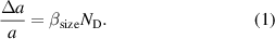
Empirically, the size effect is usually described by a parameter  which multiplies by the concentration of impurities
  to the normalized lattice parameter change Δa/a
A similar relation for the electronic contribution of free carriers via the deformation potential change is
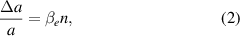
where n is the free-electron concentration. It is obvious, that different donors are described by different  , while the deformation potential effect of electrons is independent on the donor species. Romano and colleagues [6], report
  , Van de Walle (who also coauthors the Romano et al study) presents a value of
  three years later [2]. Following the ideas of Cargill et al [15] we estimate
  from the relative relaxation of neighboring atoms when introducing an impurity. These atomic relaxations are reported in reference [4] for Si and Ge in GaN and can be converted to
  and
and  , respectively.
The strength of the electronic effect described by βe in equation (2) is estimated by
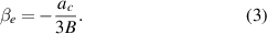
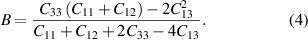
Here, ac is the deformation potential of the conduction band and B the bulk modulus of GaN which is given by the elastic constants Cij as
Depending on the choice of elastic constants  . However, for ac very different results are reported yielding consequently very different values for βe. References [2, 6] both use
  (
( and
and  ). We note, that for ac values between
  [17],
[17],  [18] and even
  [19] are discussed. Embracing also the full range of B, we consequently estimate
  . Nevertheless, it is clear that βe > 0, while
  for both donor species. Furthermore, all values for β are of the same order of magnitude, therefore the electronic and the size-effect will cancel each other out, at least partially. If we now assume
  , i.e. full donor ionization with no additional donors or compensating acceptors, we can simply add the effects up:

In case of Si, βtot is therefore expected in the interval between −1.2 × 10⁻²⁴ and  . For Ge, this range is from +1.0 × 10⁻²⁴ to
  . We want to emphasize that these values are composed from different literature reports. A comparison of different sources and our results in comparison is provided at the end of this article in table 2. Considering a very high but still realistic doping level of
  , we end up with a strain between
  and 3.2 × 10⁻⁴. Thus, the sign of the total effect is still unclear and it may even be zero by chance.
2.2. Epitaxial strain
For epitaxial samples, the strongest contribution to strain will usually arise from epitaxial strain, i.e. thermal and lattice mismatch to substrate material or template. The a-plane thin film samples investigated here have average strain values of the order of 10−3 [20]. Therefore, we have to control the epitaxial strain with very high accuracy when we want to make any claims about the influence of the size effect. Consequently, we look upon all three orthogonal lattice parameters of our samples. The definition of strain values requires definition of strain-free lattice parameters of the ideal crystal. Here, we adopt the values from reference [21], where
For the lattice parameter in m-direction, the geometrical identity  is used. The experimentally found strain is consequently defined as
Here, we develop a simple model for the strain of doped GaN taking into account both the impurity effect and the epitaxial strain effect. We exemplarily present it for the lattice parameter a but it is identical for c or m of course. We assume that the unstrained lattice parameters given in equation (6) are valid for the undoped case, i.e.  which is in line with the goal of reference [21]. We consequently assign any doped sample an altered a0(n), dependent on the dopant concentration

where a0(n = 0) is a0 from equation (6). Our samples are grown in the a-direction, this means in Hooke's law no force may be present in a-direction at the sample surface. In σ = C , the out-of-plane stress component must vanish:

Putting equations (7) and (8) into equation (9), we obtain for βtot
For a given (and carrier concentration independent) set of elastic constants, only experimental lattice parameters (a, m, and c) and the carrier concentration  have to be known to obtain βtot. Of course, equation (10) describes the situation for every donor species separately. As we investigate the donors Si and Ge, we obtain two different βtot whose difference Δβ exactly resembles the difference in
  between both donor species.
2.3. Phonon deformation potentials
As control experiments to verify our results independently, we find infrared spectroscopic ellipsometry data and Raman spectra very helpful. In the case of GaN, A1 and E1 transverse optical phonons are both infrared and Raman active and can thus be observed by both techniques. Furthermore, the infrared dielectric function yields the plasma frequency  which is directly related to the free carrier concentration n and is therefore very useful to verify the Hall effect data. The same dielectric function shows up in Raman spectra as loss function. The dielectric functions of these samples were used before to investigate the carrier dependent effective electron masses of GaN [22], the valence band dispersion [20], and the energy separation of Γ and L-points [23].
Changed lattice parameters influence the phonon eigenenergies. The interrelation is usually described by phonon deformation potentials [24]. For A1 phonons, the energy shift is given by

with the phonon deformation potentials  and
and  . For E1 phonons (and similarly for the only Raman-active E2 phonons) this equation reads

neglecting shear strain which is justified for a-oriented material. E1 phonons are more complicated to describe because of the occurrence of the additional phonon deformation potential  .
.
In the literature, different sets of phonon deformation potentials  ,
,  ,
,  ,
,  , and
, and  ,
,  are reported, however for
  (and for
  ) we could find only one report. In table 1 these results are collected. Obviously, the experimental values tabulated here for a and b agree rather well with each other for all three phonons considered.
Table 1. Phonon deformation potentials (in  ) as reported in the literature for the considered phonon modes in GaN.
| A1 | E1 | E | |
|---|---|---|---|
| a | −630 ± 40a | −820 ± 25a | −850 ± 25a |
| −640b | −717b | −742b | |
| −664 ± 129d | −850 ± 177c | ||
| −681 ± 64e | −854 ± 50e | −911 ± 54e | |
| b | −1290 ± 80a | −680 ± 50a | −920 ± 60a |
| −695b | −591b | −715b | |
| −1182 ± 282d | −963 ± 220c | ||
| −1067 ± 73e | −780 ± 70e | −852 ± 76e | |
 |
379 ± 43d | 379 ± 107d | |
| 184 ± 80f | 65 ± 20f |
a Reference [25], Raman spectroscopy b Reference [24], theory c Reference [26], Raman spectroscopy d Reference [27], Raman spectrocopy and IRSE e Reference [28], Raman spectroscopy fThis work
To connect equations (11) and (12) with experimental phonon energies ω, a strain-free eigenenergy of the respective phonon mode ω0 = ω − Δω has to be known with relatively high accuracy to avoid propagation errors in the phonon deformation potential analysis. Therefore, we investigated a strain-free a-plane cut of a free-standing GaN crystal grown by hydride vapor phase epitaxy commercially obtained from Kyma Technologies, Raleigh, as a reference first. The values for ω0 at room temperature agree well with experimental reports from the literature [29–34]. Specifically, we use  ,
,  , and
, and  .
.
3. Samples and experimental details
On the one hand, high-resolution x-ray techniques are employed to independently determine all three lattice parameters of the strained wurtzite material. On the other hand, different phonon eigenenergies are used to verify the accuracy of our results. The strain-induced shift of phonon eigenenergies is described by phonon deformation potentials which are therefore studied experimentally as well.
For this study, a set of a-plane  GaN thin films was investigated. The samples were grown by metal-organic vapor phase epitaxy on r-plane
  Al2O3 wafers. All samples are about 2.8 µm thick. The upper ≈1.4 µm of the layer was doped. One sample was unintentionally (uid) doped (Hall effect yielded
  ), four were doped by the donor silicon, and 12 were doped by the shallow donor germanium [35]. The free-electron concentration n was determined by Hall effect measurements in van-der-Pauw geometry [36], at room temperature. Selected samples were investigated by secondary ion mass spectroscopy to quantify the dopant concentration
  and no significant compensation effect was detected up to the highest free-electron concentrations. We therefore estimate
  at room temperature.
The out-of-plane lattice parameter a was measured by high resolution x-ray diffraction (HRXRD) at the symmetric GaN  Bragg reflection using a Seifert XRD 3003 HR while the in-plane lattice parameters m and c were determined by grazing incidence in-plane x-ray diffraction (GIID) at the GaN
  and GaN (0002) Bragg reflections using a modified Seifert/FPM URD6 diffractometer [37].
Phonon energies were determined by Generalized infrared spectroscopic ellipsometry [38]. using a variable-angle infrared ellipsometer (J A Woollam Co., Inc.). Two sample geometries were investigated, one with the [0001] direction in the plane of incidence and one with [0001] perpendicular to it. Thus, we obtain information about the A1(TO) and the E1(TO) phonon modes in form of point-by-point fitted dielectric functions and are able to verify the Hall effect carrier concentrations independently. More details can be found elsewhere [22]. Polarized Raman spectroscopy (S&I TriVista 777) was employed from the sample surface in different polarizer configurations. As excitation laser source, a frequency double YAG:Nd laser ( ) was used in a Raman microscope (Olympus BX51) using an objective with × 100 magnification. The laser power at the sample surface was carefully chosen to avoid sample heating. Only the Stokes side of the Raman spectra was recorded.
4. Experimental results and discussion
4.1. Lattice parameters and elastic properties
The experimentally determined lattice parameters for all three axis are shown in figure 1 as a function of free electron concentration n as determined by Hall effect measurements. While a and m lattice parameters remain approximately constant as a function of n, the c lattice parameter increases as a function of electron concentration from about  at low doping up to
  at
at  . Clearly, these experimental results violate equation (9) if the elastic constants C11, C12, and C13 and the reference lattice parameters a0, m0, and c0 are constant, i.e. free electron concentration independent.

Figure 1. Experimental lattice parameters a (open squares),  (open circles), and c (filled squares) measured by high-resolution x-ray diffraction as a function of free electron concentration n. The reference values
  and c0 are given as horizontal dashed line.
Download figure:
Standard image High-resolution imageWe visualize this fact by computing the residual out-of-plane stress σa by equation (9) as a function of n (figure 2). For the two different donor species, separate linear fits are applied and drawn as well. We want to stress that this nonzero n-dependent stress is not real. In contrast, we use σa≠ 0 to show the carrier concentration dependent effect which is very obvious in our data and which we identify as the impurity-size effect. The difference between doping by Ge and by Si is likely to be identified by the different ionic radii of the dopant cores replacing Ga in the GaN lattice, while the electronic effect has to be identical for both type of donors as discussed above.

Figure 2. Residual out-of-plane stress σa computed for constant a0, m0, and c0 as a function of free electron concentration n.
Download figure:
Standard image High-resolution imageA remaining unknown figure in our experimental result is the offset of σa at  where obviously σa must
  as no doping-induced effects are present. The here found deviation can stem from uncertainties in the elastic constants C11, C12, and C13 or wrong reference lattice parameters a0 and c0. More likely however, the presence of further defects can produce a deviation from Hooke's law in case of extended defects or a further unknown contribution to the size effect in case of further impurities not accounted for. The most likely dominating mechanism is a contribution by extended defects because all other parameters are found to be negligible. Nevertheless, the presence of extended defects, especially stacking faults in heteroepitaxial thin-film a-plane layers is no surprise [39, 40], and in our case approximately independent on the free carrier concentration as verified by studying the width of x-ray peaks. The effect of extended defects is consequently considered to be visible as an offset of
  in figure 2 independent on carrier concentration.
We use the elastic constants published in reference [41]. Applying equation (10) to all results presented in figure 1 simultaneously is equivalent to fitting βtot in equation (9) so that the slope of the regression line in figure 2 is zero. We obtain for Si  and for Ge
  .
.
Comparing this result with our discussion above is encouraging. First, the βtot value for Si is smaller than that for Ge in agreement with reference [4] and naive expectation from ionic radii. Second, the difference between both values  is nearly identical to the only available theoretical result of
  [4]. Finally, both values of βtot fit perfectly in the center of the expected range from the literature survey.
4.2. Phonons
All samples were investigated by Raman spectroscopy from the sample surface in three different Raman configurations. In Porto notation [42], these are the  geometry, where the A1(TO) and the E
 modes are visible. Next is the
  geometry with visible A1(TO) phonon only, and finally the
  geometry showing the E1(TO) phonon. In this last configuration, with crossed polarizers, small residuals of the forbidden phonon modes A1(TO) and E
 can be visible due to sample imperfections or reflected Raman forward scattering.
The peaks in the Raman spectra were fitted by a sum of Lorentzian line shapes to account for lifetime broadened phonon modes:
Here, A is the amplitude, γ the broadening, and ω0 its characteristic energy. Figure 3 presents three representative Raman spectra and the corresponding fits in the frequency range of the E1(TO) phonon mode for the  configuration. All three samples are Ge doped and a clear albeit small shift to lower frequency with increasing free electron concentration can be seen. It should be noted, that Si doped samples yield identical spectra as Ge doped samples for all phonon modes.

Figure 3. Normalized Raman spectra in  configuration of the E1(TO) phonon for three Ge doped samples with different free electron concentrations. The open circles are the experimental data, continuous curves represent the best fit. The characteristic phonon energy is marked by the vertical dotted line.
Download figure:
Standard image High-resolution imageThe same fitting is performed for Raman spectra in all configurations (for the A1(TO) phonon see figure 4) for all samples. Please note that the quality of all the fits is very good for the whole spectral range. For the further analysis, we use the phonon deformation potential set of reference [28].

Figure 4. Normalized Raman spectra in  configuration of the A1(TO) phonon for three Ge doped samples with different free electron concentrations. The open circles are the experimental data, continuous curves represent the best fit. The characteristic phonon energy is marked by the vertical dotted line.
Download figure:
Standard image High-resolution imageBecause values for the phonon deformation potentials  and
and  are missing in this set, we study the A1(TO) phonon first, where all phonon deformation potentials are known. Figure 6 presents the characteristic energy positions measured in
  configuration2, and deviations from the reference energy after applying corrections for the phonon deformation potentials and additionally the impurity-size effect, respectively. It is very obvious that the correction by phonon deformation potentials already explains most of the deviations of the experimental A1(TO) phonon mode energy from the reference value. Taking into account the impurity-size effect as well does not visibly improve the agreement. This can be explained by the relatively high scatter of the data which in turn is understandable when taking the high full-width of half maximum of the A1(TO) phonon and the presence of its anharmonic high energy shoulder [43], into account.
The same analysis for the E1(TO) phonon mode as a function of free electron concentration is shown in figure 5 (top panel) for all samples. Plotted is the difference Δω from the reference value of the E1(TO) phonon. The phonon energy shifts from about  for low doping to
  at the highest Ge concentration.

Figure 5. Characteristic phonon energy difference  from the reference value (
 shown as grey horizontal line) of the E1(TO) phonon as a function of free electron concentration n (filled symbols). The topmost panel shows the experimental results, the mid panel presents measured values corrected by phonon deformation potentials, and the bottom panel additionally corrected by the size effect.
Download figure:
Standard image High-resolution image
Figure 6. Characteristic phonon energy difference  from the reference value (
 shown as grey horizontal line) of the A1(TO) phonon as a function of free electron concentration n (filled symbols) in
  configuration. The topmost panel shows the experimental results, the mid panel presents measured values corrected by phonon deformation potentials, and the bottom panel additionally corrected by the size effect.
Download figure:
Standard image High-resolution imageCorrecting the experimental energy values by the phonon deformation potentials most of Δω vanishes (figure 5, mid panel). However at  an increasing and systematic difference Δω is visible. We claim this remaining difference to be caused by the impurity-size effect. When correcting for the size effect (separately for Ge and Si), we end up with the results shown in figure 5 (bottom panel) where except few outliers all
  . To achieve this agreement, the values of βtot for Ge and Si from above were used, but the phonon deformation potential
  was varied for minimum difference of the data points from the reference line. The result is
  . The same phonon deformation potential
  is used to plot the mid panel, too. A different value of
  would not change our results for βtot but would require a different ω0 instead.
As third phonon, we analyze the E phonon which is only Raman active (figure 7). The phonon deformation potential
  is also not reported in reference [28]. However, as visible in equation (12), the E
 phonon splits in two separate modes when
  which is fulfilled in our a-plane samples. The slope of the energy difference between both modes then equals
  . In Raman spectroscopy, we are able to observe both these modes in different configurations, namely in the
  where it should be formally forbidden and the
  configuration. Figure 8 displays the experimental results together with a linear fit (assuming no splitting for zero strain anisotropy) as a function of the strain. As result we obtain
  . Please note that the impurity-size effect does not alter this result significantly. Figure 8 is created by taking the impurity-size effect into account, but leaving it out, the result for
  is different by less then
  .
.

Figure 7. Normalized Raman spectra in  configuration of the E
 phonon for three Ge doped samples with different free electron concentrations. The open circles are the experimental data, continuous curves represent the best fit. The characteristic phonon energy is marked by the vertical dotted line.
Download figure:
Standard image High-resolution image
Figure 8. Difference Δω of the eigenenergies of E Raman-active phonons between
  and
and  measurement geometries as a function of strain difference
  . Error bars represent a very conservative maximum error of
  in the spectral position. The weighted average of the half of the slopes of the regression lines yields the phonon deformation potential
  .
.
Download figure:
Standard image High-resolution imageThe only other value for this parameter is given as  (table 1) which is on first sight not in good agreement. However, closer inspection of the source of this value [27], shows that the authors there consider it as an upper limit for
  . Therefore, our result is in agreement with the result from reference [27].
The impurity-size effect is not obvious in figure 8 because nearly unaffected  form the abscissa. The influence of the impurity-size effect is thus visualized in figure 9. The overall agreement of the shifted data points with the
  line is slightly worse compared to the cases of the A1(TO) or E1(TO) phonons, especially at lower free-carrier concentrations. Because here,
  and the values for βtot are obtained earlier with high accuracy and are simply entering the calculation, the remaining offset from the reference value might stem from (i) a slightly offset ω0, (ii) propagation errors due to the used phonon deformation potentials or (iii) additional effects shifting the E
 mode in our samples not covered by our model. Inspecting table 1 we find that the used phonon deformation potential set [28], for the E
 mode is the only experimental one having
  . Nevertheless, the agreement of model and experimental data is still very satisfying. A final judgment on the remaining small differences is not achievable in the framework of our study.

Figure 9. Characteristic phonon energy difference  from the reference value (
 shown as grey horizontal line) of the E
 phonon as a function of free electron concentration n (filled symbols) in
  configuration. The topmost panel shows the experimental results, the mid panel presents measured values corrected by phonon deformation potentials, and the bottom panel additionally corrected by the size effect.
Download figure:
Standard image High-resolution image5. Summary
In conclusion, by investigating lattice parameters and phonon energies of nonpolar a-plane GaN films with different dopant concentrations, we obtain experimental results for the impurity-size effects of Si and Ge in GaN. This effect is inseparably composed of the size-effect and the electronic deformation potential contribution. For the latter, an interval between  seems reliable, however this contribution is identical for both dopant species. Thus, we are able to compare our experimental results to values from the literature (table 2).
Table 2. Different isotropically averaged impurity-size effect parameters βtot for Si and Ge in wurtzite GaN (in  ). We took only βsize from the references and added βe ourselves. The error bars account for the range of possible βe values.
| Si | Ge | |
|---|---|---|
| reference [4] | 0.8 ± 1.1 | 2.1 ± 1.1 |
| reference [6] | 0.9 ± 1.1 | |
| reference [2] | −0.1 ± 1.1 | |
| This work | 0.7 | 1.9 |
By analyzing the phonon energies of the anisotropically strained layers, we are furthermore able to obtain reliable values for the phonon deformation potentials  and
and  . These values are compared to literature results in table 1.
Acknowledgment
We gratefully acknowledge support by the Deutsche Forschungsgemeinschaft in the framework of Major Research Instrumentation Program No. INST 272/230-1.
Footnotes
- 2
The difference in characteristic A1(TO) phonon energies between the
 and the configuration is very small (except outliers ), not systematic as a function of free electron concentration, and not different between GaN:Si and GaN:Ge. We therefore concentrate on the configuration where this phonon is found in higher intensity and exclusively.


