当前位置:
X-MOL 学术
›
Chem. Rev.
›
论文详情
Our official English website, www.x-mol.net, welcomes your feedback! (Note: you will need to create a separate account there.)
Quantum and Dielectric Confinement Effects in Lower-Dimensional Hybrid Perovskite Semiconductors
Chemical Reviews ( IF 62.1 ) Pub Date : 2019-01-14 00:00:00 , DOI: 10.1021/acs.chemrev.8b00417 Claudine Katan 1 , Nicolas Mercier 2 , Jacky Even 3
Chemical Reviews ( IF 62.1 ) Pub Date : 2019-01-14 00:00:00 , DOI: 10.1021/acs.chemrev.8b00417 Claudine Katan 1 , Nicolas Mercier 2 , Jacky Even 3
Affiliation
|
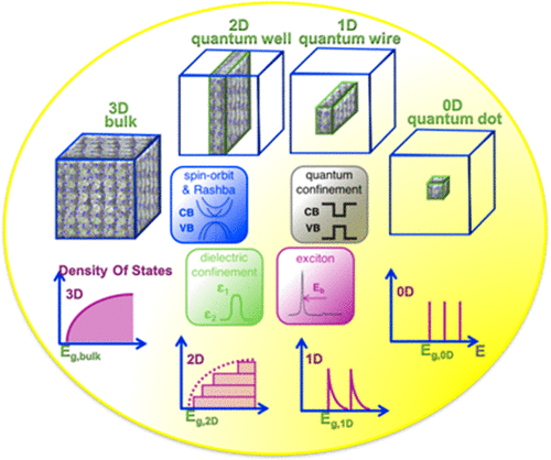
Hybrid halide perovskites are now superstar materials leading the field of low-cost thin film photovoltaics technologies. Following the surge for more efficient and stable 3D bulk alloys, multilayered halide perovskites and colloidal perovskite nanostructures appeared in 2016 as viable alternative solutions to this challenge, largely exceeding the original proof of concept made in 2009 and 2014, respectively. This triggered renewed interest in lower-dimensional hybrid halide perovskites and at the same time increasingly more numerous and differentiated applications. The present paper is a review of the past and present literature on both colloidal nanostructures and multilayered compounds, emphasizing that availability of accurate structural information is of dramatic importance to reach a fair understanding of quantum and dielectric confinement effects. Layered halide perovskites occupy a special place in the history of halide perovskites, with a large number of seminal papers in the 1980s and 1990s. In recent years, the rationalization of structure–properties relationship has greatly benefited from new theoretical approaches dedicated to their electronic structures and optoelectronic properties, as well as a growing number of contributions based on modern experimental techniques. This is a necessary step to provide in-depth tools to decipher their extensive chemical engineering possibilities which surpass the ones of their 3D bulk counterparts. Comparisons to classical semiconductor nanostructures and 2D van der Waals heterostructures are also stressed. Since 2015, colloidal nanostructures have undergone a quick development for applications based on light emission. Although intensively studied in the last two years by various spectroscopy techniques, the description of quantum and dielectric confinement effects on their optoelectronic properties is still in its infancy.
中文翻译:

低维混合钙钛矿半导体中的量子和介电限制效应
混合卤化物钙钛矿现已成为引领低成本薄膜光伏技术领域的超级明星材料。随着更高效,更稳定的3D块状合金激增,多层卤化物钙钛矿和胶体钙钛矿纳米结构在2016年成为应对这一挑战的可行替代解决方案,大大超过了分别在2009年和2014年提出的概念证明。这引起了人们对低维杂化卤化物钙钛矿的新兴趣,同时也引起了越来越多的差异化应用。本文是对胶体纳米结构和多层化合物既往文献的回顾,强调提供准确的结构信息对于公平理解量子和介电限制效应至关重要。层状卤化物钙钛矿在卤化物钙钛矿的历史上占有特殊的地位,在1980年代和1990年代有大量开创性论文。近年来,结构-性能关系的合理化已从受益于专用于其电子结构和光电特性的新理论方法,以及基于现代实验技术的越来越多的贡献中受益。这是提供深入工具以破译其广泛的化学工程可能性的必要步骤,而这种可能性超过了其3D体模型的可能性。还强调了与经典半导体纳米结构和2D范德华异质结构的比较。自2015年以来,胶体纳米结构在基于发光的应用方面得到了快速发展。尽管在最近两年中通过各种光谱技术进行了深入研究,但有关量子和介电限制效应对其光电性能的描述仍处于起步阶段。
更新日期:2019-01-14
中文翻译:
低维混合钙钛矿半导体中的量子和介电限制效应
混合卤化物钙钛矿现已成为引领低成本薄膜光伏技术领域的超级明星材料。随着更高效,更稳定的3D块状合金激增,多层卤化物钙钛矿和胶体钙钛矿纳米结构在2016年成为应对这一挑战的可行替代解决方案,大大超过了分别在2009年和2014年提出的概念证明。这引起了人们对低维杂化卤化物钙钛矿的新兴趣,同时也引起了越来越多的差异化应用。本文是对胶体纳米结构和多层化合物既往文献的回顾,强调提供准确的结构信息对于公平理解量子和介电限制效应至关重要。层状卤化物钙钛矿在卤化物钙钛矿的历史上占有特殊的地位,在1980年代和1990年代有大量开创性论文。近年来,结构-性能关系的合理化已从受益于专用于其电子结构和光电特性的新理论方法,以及基于现代实验技术的越来越多的贡献中受益。这是提供深入工具以破译其广泛的化学工程可能性的必要步骤,而这种可能性超过了其3D体模型的可能性。还强调了与经典半导体纳米结构和2D范德华异质结构的比较。自2015年以来,胶体纳米结构在基于发光的应用方面得到了快速发展。尽管在最近两年中通过各种光谱技术进行了深入研究,但有关量子和介电限制效应对其光电性能的描述仍处于起步阶段。


 京公网安备 11010802027423号