当前位置:
X-MOL 学术
›
Adv. Mater.
›
论文详情
Our official English website, www.x-mol.net, welcomes your feedback! (Note: you will need to create a separate account there.)
Ultrahigh‐Sensitive Broadband Photodetectors Based on Dielectric Shielded MoTe2/Graphene/SnS2 p–g–n Junctions
Advanced Materials ( IF 29.4 ) Pub Date : 2018-12-14 , DOI: 10.1002/adma.201805656 Alei Li 1, 2 , Qianxue Chen 1 , Peipei Wang 1 , Yuan Gan 1 , Tailei Qi 1 , Peng Wang 1 , Fangdong Tang 1 , Judy Z. Wu 3 , Rui Chen 4 , Liyuan Zhang 1 , Youpin Gong 1, 4, 5
Advanced Materials ( IF 29.4 ) Pub Date : 2018-12-14 , DOI: 10.1002/adma.201805656 Alei Li 1, 2 , Qianxue Chen 1 , Peipei Wang 1 , Yuan Gan 1 , Tailei Qi 1 , Peng Wang 1 , Fangdong Tang 1 , Judy Z. Wu 3 , Rui Chen 4 , Liyuan Zhang 1 , Youpin Gong 1, 4, 5
Affiliation
|
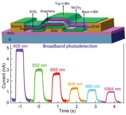
2D atomic sheets of transition metal dichalcogenides (TMDs) have a tremendous potential for next‐generation optoelectronics since they can be stacked layer‐by‐layer to form van der Waals (vdW) heterostructures. This allows not only bypassing difficulties in heteroepitaxy of lattice‐mismatched semiconductors of desired functionalities but also providing a scheme to design new optoelectronics that can surpass the fundamental limitations on their conventional semiconductor counterparts. Herein, a novel 2D h‐BN/p‐MoTe2/graphene/n‐SnS2/h‐BN p–g–n junction, fabricated by a layer‐by‐layer dry transfer, demonstrates high‐sensitivity, broadband photodetection at room temperature. The combination of the MoTe2 and SnS2 of complementary bandgaps, and the graphene interlayer provides a unique vdW heterostructure with a vertical built‐in electric field for high‐efficiency broadband light absorption, exciton dissociation, and carrier transfer. The graphene interlayer plays a critical role in enhancing sensitivity and broadening the spectral range. An optimized device containing 5−7‐layer graphene has been achieved and shows an extraordinary responsivity exceeding 2600 A W−1 with fast photoresponse and specific detectivity up to ≈1013 Jones in the ultraviolet–visible–near‐infrared spectrum. This result suggests that the vdW p–g–n junctions containing multiple photoactive TMDs can provide a viable approach toward future ultrahigh‐sensitivity and broadband photonic detectors.
中文翻译:

基于介电屏蔽MoTe2 /石墨烯/ SnS2 p–g–n结的超高灵敏度宽带光电探测器
过渡金属二硫化碳(TMD)的二维原子片具有下一代光电的巨大潜力,因为它们可以逐层堆叠以形成范德华(vdW)异质结构。这不仅可以绕开具有所需功能的晶格不匹配半导体的异质外延困难,而且可以提供一种设计新的光电技术的方案,该方案可以超越其常规半导体同类产品的基本限制。本文中,通过逐层干转移制备的新型2D h-BN / p-MoTe 2 /石墨烯/ n-SnS 2 / h-BN p-g-n结表现出高灵敏度,宽带光检测室内温度。MoTe 2和SnS 2的组合的互补带隙,并且石墨烯夹层提供了独特的vdW异质结构,具有垂直的内置电场,可实现高效宽带光吸收,激子离解和载流子转移。石墨烯夹层在提高灵敏度和扩大光谱范围方面起着关键作用。含有5-7层石墨烯的优化的设备已经实现了,并显示一个非凡的响应度超过2600 AW -1具有快速光响应和比探测到≈10 13和在紫外线-可见光-近红外光谱琼斯。该结果表明,包含多个光敏TMD的vdW p–g–n结点可以为未来的超高灵敏度和宽带光子探测器提供可行的方法。
更新日期:2018-12-14
中文翻译:
基于介电屏蔽MoTe2 /石墨烯/ SnS2 p–g–n结的超高灵敏度宽带光电探测器
过渡金属二硫化碳(TMD)的二维原子片具有下一代光电的巨大潜力,因为它们可以逐层堆叠以形成范德华(vdW)异质结构。这不仅可以绕开具有所需功能的晶格不匹配半导体的异质外延困难,而且可以提供一种设计新的光电技术的方案,该方案可以超越其常规半导体同类产品的基本限制。本文中,通过逐层干转移制备的新型2D h-BN / p-MoTe 2 /石墨烯/ n-SnS 2 / h-BN p-g-n结表现出高灵敏度,宽带光检测室内温度。MoTe 2和SnS 2的组合的互补带隙,并且石墨烯夹层提供了独特的vdW异质结构,具有垂直的内置电场,可实现高效宽带光吸收,激子离解和载流子转移。石墨烯夹层在提高灵敏度和扩大光谱范围方面起着关键作用。含有5-7层石墨烯的优化的设备已经实现了,并显示一个非凡的响应度超过2600 AW -1具有快速光响应和比探测到≈10 13和在紫外线-可见光-近红外光谱琼斯。该结果表明,包含多个光敏TMD的vdW p–g–n结点可以为未来的超高灵敏度和宽带光子探测器提供可行的方法。


 京公网安备 11010802027423号