当前位置:
X-MOL 学术
›
J. Am. Chem. Soc.
›
论文详情
Our official English website, www.x-mol.net, welcomes your feedback! (Note: you will need to create a separate account there.)
III-V Clathrate Semiconductors with Outstanding Hole Mobility: Cs8In27Sb19 and A8Ga27Sb19 (A = Cs, Rb)
Journal of the American Chemical Society ( IF 15.0 ) Pub Date : 2020-01-02 , DOI: 10.1021/jacs.9b12351 Bryan Owens-Baird 1, 2 , Jian Wang 1, 2, 3 , Suyin Grass Wang 4 , Yu-Sheng Chen 4 , Shannon Lee 1, 2 , Davide Donadio 5 , Kirill Kovnir 1, 2
Journal of the American Chemical Society ( IF 15.0 ) Pub Date : 2020-01-02 , DOI: 10.1021/jacs.9b12351 Bryan Owens-Baird 1, 2 , Jian Wang 1, 2, 3 , Suyin Grass Wang 4 , Yu-Sheng Chen 4 , Shannon Lee 1, 2 , Davide Donadio 5 , Kirill Kovnir 1, 2
Affiliation
|
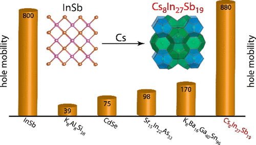
Three novel unconventional clathrates with unprecedented III-V semiconducting frameworks have been synthesized: Cs8In27Sb19, Cs8Ga27Sb19, and Rb8Ga27Sb19. These clathrates represent the first examples of tetrel-free clathrates that are completely composed of main group elements. All title compounds crystallize in an ordered superstructure of clathrate-I in the Ia-3 space group (No. 206; Z = 8). In the clathrate framework, a full ordering of {Ga or In} and Sb is observed by a combination of high-resolution synchrotron single-crystal and powder X-ray diffraction techniques. Density functional theory (DFT) calculations show that all three clathrates are energetically stable with relaxed lattice constants matching the experimental data. Due to the complexity of the crystal structure composed of heavy elements, the reported clathrates exhibit ultralow thermal conductivities of less than 1 W/(m∙K) at room temperature. All compounds are predicted and experimentally confirmed to be narrow-bandgap p-type semiconductors with high Seebeck thermopower values, up to 250 μV/K at 300 K for Cs8In27Sb19. The latter compound shows carrier concentrations and mobilities, 1.42x10^15 cm^-3 and 880 cm^2/(V∙s), which are on par with the values for parent binary InSb, one of the best electronic semiconductors. The high hole carrier mobility is uncommon for complex bulk materials and a highly desirable trait, opening ways to design semiconducting materials based on tunable III-V clathrates.
中文翻译:

具有出色空穴迁移率的 III-V 包合物半导体:Cs8In27Sb19 和 A8Ga27Sb19 (A = Cs, Rb)
已经合成了三种具有前所未有的 III-V 半导体骨架的新型非常规包合物:Cs8In27Sb19、Cs8Ga27Sb19 和 Rb8Ga27Sb19。这些包合物代表了完全由主族元素组成的无 tetrel 包合物的第一个例子。所有标题化合物都在 Ia-3 空间群(No. 206;Z = 8)的笼形 I 的有序超结构中结晶。在包合物框架中,通过高分辨率同步加速器单晶和粉末 X 射线衍射技术的组合观察到 {Ga 或 In} 和 Sb 的完全有序。密度泛函理论 (DFT) 计算表明,所有三种包合物都是能量稳定的,松弛晶格常数与实验数据相匹配。由于重元素组成的晶体结构复杂,报道的包合物在室温下表现出低于 1 W/(m∙K) 的超低热导率。所有化合物都被预测并通过实验证实是具有高塞贝克热电值的窄带隙 p 型半导体,Cs8In27Sb19 在 300 K 时高达 250 μV/K。后一种化合物的载流子浓度和迁移率分别为 1.42x10^15 cm^-3 和 880 cm^2/(V∙s),与母体二元 InSb(最好的电子半导体之一)的值相当。高空穴载流子迁移率对于复杂的体材料和非常理想的特性来说并不常见,这为设计基于可调谐 III-V 包合物的半导体材料开辟了道路。所有化合物都被预测并通过实验证实是窄带隙 p 型半导体,具有高塞贝克热电值,Cs8In27Sb19 在 300 K 时高达 250 μV/K。后一种化合物的载流子浓度和迁移率分别为 1.42x10^15 cm^-3 和 880 cm^2/(V∙s),与母体二元 InSb(最好的电子半导体之一)的值相当。高空穴载流子迁移率对于复杂的体材料和非常理想的特性来说并不常见,这为设计基于可调谐 III-V 包合物的半导体材料开辟了道路。所有化合物都被预测并通过实验证实是具有高塞贝克热电值的窄带隙 p 型半导体,Cs8In27Sb19 在 300 K 时高达 250 μV/K。后一种化合物的载流子浓度和迁移率分别为 1.42x10^15 cm^-3 和 880 cm^2/(V∙s),与母体二元 InSb(最好的电子半导体之一)的值相当。高空穴载流子迁移率对于复杂的体材料和非常理想的特性来说并不常见,这为设计基于可调谐 III-V 包合物的半导体材料开辟了道路。
更新日期:2020-01-02
中文翻译:
具有出色空穴迁移率的 III-V 包合物半导体:Cs8In27Sb19 和 A8Ga27Sb19 (A = Cs, Rb)
已经合成了三种具有前所未有的 III-V 半导体骨架的新型非常规包合物:Cs8In27Sb19、Cs8Ga27Sb19 和 Rb8Ga27Sb19。这些包合物代表了完全由主族元素组成的无 tetrel 包合物的第一个例子。所有标题化合物都在 Ia-3 空间群(No. 206;Z = 8)的笼形 I 的有序超结构中结晶。在包合物框架中,通过高分辨率同步加速器单晶和粉末 X 射线衍射技术的组合观察到 {Ga 或 In} 和 Sb 的完全有序。密度泛函理论 (DFT) 计算表明,所有三种包合物都是能量稳定的,松弛晶格常数与实验数据相匹配。由于重元素组成的晶体结构复杂,报道的包合物在室温下表现出低于 1 W/(m∙K) 的超低热导率。所有化合物都被预测并通过实验证实是具有高塞贝克热电值的窄带隙 p 型半导体,Cs8In27Sb19 在 300 K 时高达 250 μV/K。后一种化合物的载流子浓度和迁移率分别为 1.42x10^15 cm^-3 和 880 cm^2/(V∙s),与母体二元 InSb(最好的电子半导体之一)的值相当。高空穴载流子迁移率对于复杂的体材料和非常理想的特性来说并不常见,这为设计基于可调谐 III-V 包合物的半导体材料开辟了道路。所有化合物都被预测并通过实验证实是窄带隙 p 型半导体,具有高塞贝克热电值,Cs8In27Sb19 在 300 K 时高达 250 μV/K。后一种化合物的载流子浓度和迁移率分别为 1.42x10^15 cm^-3 和 880 cm^2/(V∙s),与母体二元 InSb(最好的电子半导体之一)的值相当。高空穴载流子迁移率对于复杂的体材料和非常理想的特性来说并不常见,这为设计基于可调谐 III-V 包合物的半导体材料开辟了道路。所有化合物都被预测并通过实验证实是具有高塞贝克热电值的窄带隙 p 型半导体,Cs8In27Sb19 在 300 K 时高达 250 μV/K。后一种化合物的载流子浓度和迁移率分别为 1.42x10^15 cm^-3 和 880 cm^2/(V∙s),与母体二元 InSb(最好的电子半导体之一)的值相当。高空穴载流子迁移率对于复杂的体材料和非常理想的特性来说并不常见,这为设计基于可调谐 III-V 包合物的半导体材料开辟了道路。


 京公网安备 11010802027423号