Applied Materials Today ( IF 8.3 ) Pub Date : 2019-12-28 , DOI: 10.1016/j.apmt.2019.100541 Muhammad Ali Johar , Hyun-Gyu Song , Aadil Waseem , Mostafa Afifi Hassan , Indrajit V. Bagal , Yong-Hoon Cho , Sang-Wan Ryu
|
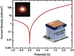
GaN-based light-emitting diodes (LEDs) on sapphire are known to exhibit high efficiency and long lifetime. Currently, Si substrate has been explored for the replacement of sapphire substrate due to the size limitations. In order to fabricate the cost-effective LEDs on larger scale, the most efficient approach is the growth of scalable and high crystal quality GaN nanowires on amorphous substrate, preferably glass. Here, for the first time, we have demonstrated the growth of GaN nanowire-based LEDs using metal-organic chemical vapor deposition (MOCVD) on an amorphous glass substrate. Additionally, the InGaN/GaN multiple quantum well shells are conformally grown on semipolar { growth facet of m-axial GaN core nanowires and resulted in reduced quantum confined Stark effect. The optical properties of the nanowire-ensemble are rigorously evaluated by both temperature-dependent and time-resolved photoluminescence (PL), whereas the emission from the single nanowire is examined by spatially resolved cathodoluminescence. The PL spectroscopy of the GaN core nanowire-ensemble reveals a very high crystal quality due to the dominant emission from the band-to-band transition and absence of a characteristic yellow luminescence. Furthermore, the temperature-dependent PL of the nanowire ensemble exhibits a very high internal quantum efficiency of 76.1 %. Therefore, the ultrashort radiative lifetime of the carriers was in the range between 19 ps and 54 ps. These results emphasize the potential of our approach to grow high-crystal quality GaN nanowires on amorphous substrates for large scale production and various optical applications such as LEDs, solar cells, and photodetectors.
中文翻译:
通过MOCVD在非晶衬底上制造基于GaN纳米线的LED的通用且可扩展的路线
蓝宝石上的GaN基发光二极管(LED)已知具有高效率和长寿命。当前,由于尺寸限制,已经研究了Si衬底来代替蓝宝石衬底。为了大规模制造具有成本效益的LED,最有效的方法是在无定形基板(最好是玻璃)上生长可缩放且具有高晶体质量的GaN纳米线。在这里,我们首次展示了使用非晶有机玻璃基板上的金属有机化学气相沉积(MOCVD)技术来生长基于GaN纳米线的LED。此外,InGaN / GaN多量子阱壳在半极性{m轴GaN核纳米线的生长面,并导致减小的量子限制Stark效应。纳米线集合体的光学性质通过温度依赖性和时间分辨的光致发光(PL)进行严格评估,而单个纳米线的发射则通过空间分辨的阴极发光来检查。GaN核纳米线整体的PL光谱显示出非常高的晶体质量,这是由于带间跃迁的主要发射和缺乏特征性的黄色发光所致。此外,纳米线系的依赖温度的PL表现出76.1%的非常高的内部量子效率。因此,载流子的超短辐射寿命在19 ps和54 ps之间。


 京公网安备 11010802027423号