当前位置:
X-MOL 学术
›
ACS Appl. Nano Mater.
›
论文详情
Our official English website, www.x-mol.net, welcomes your feedback! (Note: you will need to create a separate account there.)
The Geode Process: Hollow Silica Microcapsules as a High Surface Area Substrate for Semiconductor Nanowire Growth
ACS Applied Nano Materials ( IF 5.9 ) Pub Date : 2020-01-10 , DOI: 10.1021/acsanm.9b02553 Maritza Mujica 1 , Gozde Tutuncuoglu 1 , Pralav P. Shetty 2 , Amar T. Mohabir 1 , Eric V. Woods 3 , Victor Breedveld 1 , Sven H. Behrens 1 , Michael A. Filler 1
ACS Applied Nano Materials ( IF 5.9 ) Pub Date : 2020-01-10 , DOI: 10.1021/acsanm.9b02553 Maritza Mujica 1 , Gozde Tutuncuoglu 1 , Pralav P. Shetty 2 , Amar T. Mohabir 1 , Eric V. Woods 3 , Victor Breedveld 1 , Sven H. Behrens 1 , Michael A. Filler 1
Affiliation
|
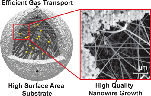
We introduce and demonstrate critical steps toward the Geode process for the bottom-up synthesis of semiconductor nanowires. Central to the process is the design and fabrication of an unconventional, high surface area substrate: the interior surface of hollow silica microcapsules, assembled from silica particles via emulsion templating, and featuring porous walls to enable efficient gas transport. The interior surface of these hollow silica microcapsules is decorated with gold nanoparticles that seed nanowire growth via the vapor–liquid–solid (VLS) mechanism. We demonstrate the production of the necessary microcapsules and show how microcapsule structure and stability upon drying are influenced by the type of silica particles and use of a particle cross-linking agent. Finally, we demonstrate the synthesis of crystalline Si nanowires in the microcapsule interior.
中文翻译:

Geode工艺:中空二氧化硅微胶囊作为半导体纳米线生长的高表面积基质
我们介绍并演示了从根本上合成半导体纳米线的Geode工艺的关键步骤。该过程的中心是非常规高表面积基材的设计和制造:空心二氧化硅微胶囊的内表面,是通过乳液模板由二氧化硅颗粒组装而成的,并具有多孔壁以实现有效的气体传输。这些空心二氧化硅微胶囊的内表面装饰有金纳米颗粒,这些纳米颗粒通过气-液-固(VLS)机理为纳米线的生长提供了种子。我们演示了必要的微胶囊的生产,并展示了微胶囊的结构和干燥后的稳定性如何受到二氧化硅颗粒类型和颗粒交联剂使用的影响。最后,
更新日期:2020-01-10
中文翻译:
Geode工艺:中空二氧化硅微胶囊作为半导体纳米线生长的高表面积基质
我们介绍并演示了从根本上合成半导体纳米线的Geode工艺的关键步骤。该过程的中心是非常规高表面积基材的设计和制造:空心二氧化硅微胶囊的内表面,是通过乳液模板由二氧化硅颗粒组装而成的,并具有多孔壁以实现有效的气体传输。这些空心二氧化硅微胶囊的内表面装饰有金纳米颗粒,这些纳米颗粒通过气-液-固(VLS)机理为纳米线的生长提供了种子。我们演示了必要的微胶囊的生产,并展示了微胶囊的结构和干燥后的稳定性如何受到二氧化硅颗粒类型和颗粒交联剂使用的影响。最后,


 京公网安备 11010802027423号