当前位置:
X-MOL 学术
›
Nano Lett.
›
论文详情
Our official English website, www.x-mol.net, welcomes your feedback! (Note: you will need to create a separate account there.)
Synthetic Semimetals with van der Waals Interfaces.
Nano Letters ( IF 10.8 ) Pub Date : 2020-01-02 , DOI: 10.1021/acs.nanolett.9b04810 Bojja Aditya Reddy 1, 2 , Evgeniy Ponomarev 1, 2 , Ignacio Gutiérrez-Lezama 1, 2 , Nicolas Ubrig 1, 2 , Céline Barreteau 1, 3 , Enrico Giannini 1 , Alberto F Morpurgo 1, 2
Nano Letters ( IF 10.8 ) Pub Date : 2020-01-02 , DOI: 10.1021/acs.nanolett.9b04810 Bojja Aditya Reddy 1, 2 , Evgeniy Ponomarev 1, 2 , Ignacio Gutiérrez-Lezama 1, 2 , Nicolas Ubrig 1, 2 , Céline Barreteau 1, 3 , Enrico Giannini 1 , Alberto F Morpurgo 1, 2
Affiliation
|
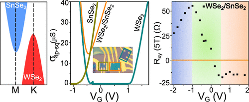
The assembly of suitably designed van der Waals (vdW) heterostructures represents a new approach to produce artificial systems with engineered electronic properties. Here, we apply this strategy to realize synthetic semimetals based on vdW interfaces formed by two different semiconductors. Guided by existing ab initio calculations, we select WSe2 and SnSe2 mono- and multilayers to assemble vdW interfaces and demonstrate the occurrence of semimetallicity by means of different transport experiments. Semimetallicity manifests itself in a finite minimum conductance upon sweeping the gate over a large range in ionic liquid gated devices, which also offer spectroscopic capabilities enabling the quantitative determination of the band overlap. The semimetallic state is additionally revealed in Hall effect measurements by the coexistence of electrons and holes, observed by either looking at the evolution of the Hall slope with sweeping the gate voltage or with lowering temperature. Finally, semimetallicity results in the low-temperature metallic conductivity of interfaces of two materials that are themselves insulating. These results demonstrate the possibility to implement a state of matter that had not yet been realized in vdW interfaces and represent a first step toward using these interfaces to engineer topological or excitonic insulating states.
中文翻译:

具有范德华界面的合成半金属。
适当设计的范德华(vdW)异质结构的组装代表了一种生产具有工程电子特性的人工系统的新方法。在这里,我们将这种策略应用于基于由两种不同半导体形成的vdW界面的合成半金属。在现有的从头算计算的指导下,我们选择WSe2和SnSe2单层和多层来组装vdW界面,并通过不同的传输实验证明半金属性的发生。半金属性在离子液体门控器件中在大范围内扫描栅极时表现为有限的最小电导,这还提供了能够定量确定带重叠的光谱功能。在霍尔效应测量中,电子和空穴的共存还揭示了半金属态,可以通过扫描栅极电压或降低温度来观察霍尔斜率的变化来观察。最后,半金属性导致两种材料的界面的低温金属导电性,而这两种材料本身是绝缘的。这些结果证明了在vdW界面中实现尚未实现的物质状态的可能性,并代表着朝着使用这些界面设计拓扑或激子绝缘态的第一步。半金属性导致两种本身绝缘的材料的界面具有低温金属导电性。这些结果证明了实现尚未在vdW接口中实现的物质状态的可能性,并且代表着朝着使用这些接口设计拓扑或激子绝缘状态的第一步。半金属性导致两种本身绝缘的材料的界面具有低温金属导电性。这些结果证明了在vdW界面中实现尚未实现的物质状态的可能性,并代表着朝着使用这些界面设计拓扑或激子绝缘态的第一步。
更新日期:2020-01-04
中文翻译:
具有范德华界面的合成半金属。
适当设计的范德华(vdW)异质结构的组装代表了一种生产具有工程电子特性的人工系统的新方法。在这里,我们将这种策略应用于基于由两种不同半导体形成的vdW界面的合成半金属。在现有的从头算计算的指导下,我们选择WSe2和SnSe2单层和多层来组装vdW界面,并通过不同的传输实验证明半金属性的发生。半金属性在离子液体门控器件中在大范围内扫描栅极时表现为有限的最小电导,这还提供了能够定量确定带重叠的光谱功能。在霍尔效应测量中,电子和空穴的共存还揭示了半金属态,可以通过扫描栅极电压或降低温度来观察霍尔斜率的变化来观察。最后,半金属性导致两种材料的界面的低温金属导电性,而这两种材料本身是绝缘的。这些结果证明了在vdW界面中实现尚未实现的物质状态的可能性,并代表着朝着使用这些界面设计拓扑或激子绝缘态的第一步。半金属性导致两种本身绝缘的材料的界面具有低温金属导电性。这些结果证明了实现尚未在vdW接口中实现的物质状态的可能性,并且代表着朝着使用这些接口设计拓扑或激子绝缘状态的第一步。半金属性导致两种本身绝缘的材料的界面具有低温金属导电性。这些结果证明了在vdW界面中实现尚未实现的物质状态的可能性,并代表着朝着使用这些界面设计拓扑或激子绝缘态的第一步。


 京公网安备 11010802027423号